Electron spin blockade and singlet-triplet transition in a silicon single electron transistor
Abstract
We investigate a silicon single-electron transistor (SET) in a metal-oxide-semiconductor (MOS) structure by applying a magnetic field perpendicular to the sample surface. The quantum dot is defined electrostatically in a point contact channel and by the potential barriers from negatively charged interface traps. The magnetic field dependence of the excitation spectrum is primarily driven by the Zeeman effect. In the two-electron singlet-triplet (ST) transition, electron-electron Coulomb interaction plays a significant role. The evolution of Coulomb blockade peaks with magnetic field is also owing to the Zeeman splitting with no obvious orbital effect up to 9 T. The filling pattern shows an alternate spin-up-spin-down sequence. The amplitude spectroscopy allows for the observation of the spin blockade effect, where the two-electron system forms a singlet state at low fields, and the spin polarized injection from the lead reduces the tunneling conductance by a factor of 8. At a higher magnetic field, due to the ST transition, the spin blockade effect is lifted and the conductance is fully recovered.
pacs:
73.23.Hk, 72.25.-b, 73.40.QvI INTRODUCTION
As a promising candidate of spin qubits for quantum computing, semiconductor quantum dots have attracted tremendous research effort.Loss and DiVincenzo (1998) Recent progress in GaAs lateral quantum dots has demonstrated all possible single-qubit operationsKoppens et al. (2006) and the square-root-of-swap operation on two qubits,Petta et al. (2005) which form a universal set for quantum computing.Loss and DiVincenzo (1998) Compared to GaAs, lateral quantum dots in 28silicon are expected to have a spin coherence time orders of magnitudes longer, because 28Si has no nuclear spin, and there is no hyperfine interaction between electron spins and nuclear spins.Feher (1959) There has been steady progress in the development of silicon-based single electron transistors using silicon-on-insulator (SOI) wafers,Fujiwara et al. (2006) Si/SiGe quantum well structuresSimmons et al. (2007) and metal-oxide-semiconductor (MOS) structures,Jones et al. (2006); Angus et al. (2007) though it remains a considerable challenge due to material properties.Jones et al. (2006)
In this paper, we present our recent progress on an enhancement-mode MOS single electron transistor (SET) in pure silicon.Jones et al. (2006) The unique structure of the MOS-SET allows us to verify the formation of quantum dots and better understand the device, which is largely neglected in some early works. When properly biased, the investigated SET has a quantum dot in an electrostatically defined point contact channel. In addition to single electron tunneling behavior, we have also observed its magnetic field dependence. For all of the data presented here, the field is applied perpendicular to the sample surface. The observed magnetic field dependence of the excitation spectrumKouwenhoven et al. (2001) is found to be primarily driven by the Zeeman splitting. Furthermore, the spectrum enables us to directly observe the singlet-triplet (ST) transition, where electron-electron Coulomb interaction plays a significant role. The evolution of Coulomb blockade peaks with the magnetic field is also measured. The data strongly suggest that the ground state energies also shift with the applied magnetic field owing to the Zeeman effect. Up to 9 T, there is no obvious orbital effect. The evolution of peak amplitudes illustrates the spin blockade effect due to magnetic field induced spatial separation of spin-up and spin-down states. At a higher magnetic field, the spin blockade effect is lifted when the SET undergoes the ST transition.
II SAMPLES AND TRANSPORT CHARACTERISTICS
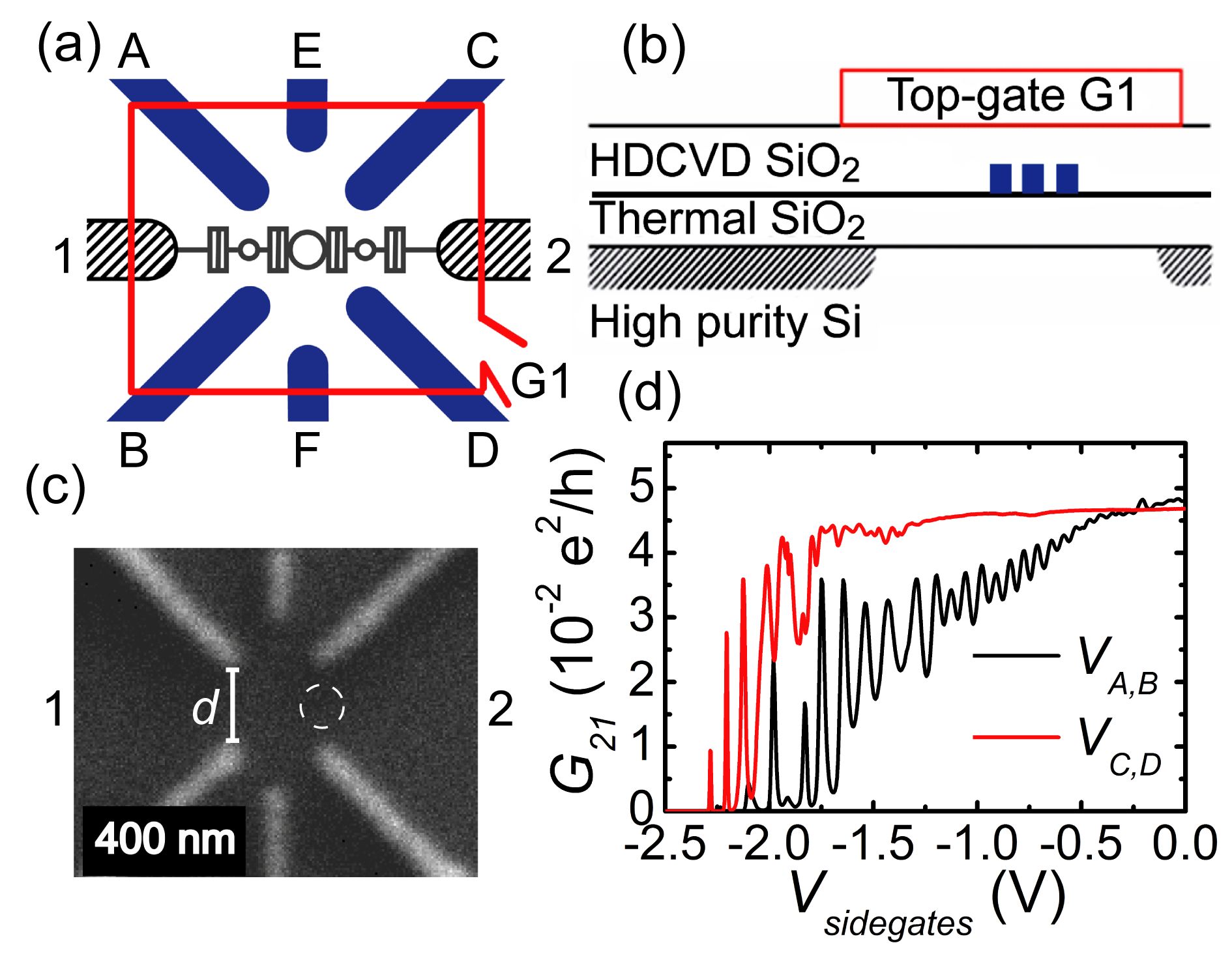
Figures 1(a) and 1(b) show the schematic top view and the cross-sectional view of the device. All devices are fabricated on N-type, high purity silicon (100) wafers with a resistivity of km. By using photolithography and ion implantation, the heavily phosphorous-doped regions are defined as the source (1) and the drain (2). A 27 nm thick thermal oxide is grown by dry oxidation. It also has a bilayer-gated configuration. Six side gates (labeled as A-F in Fig. 1(a)) are located above the thermal oxide and buried in the second dielectric layer, SiO2, which is 400 nm in thickness and grown by high-density plasma-enhanced chemical vapor deposition (HDPECVD). The top gate (G1), which is above the HDPECVD oxide, laterally overlaps with the ohmic source and drain regions. The device is annealed in forming gas at 420 ∘C for 30 minutes to reduce the interface states. The fabrication process and the basic operating principle have been discussed in more detail elsewhere.Jones et al. (2006) These devices are characterized in a dilution refrigerator with 10 mK base temperature. The electron temperature is about 400 mK by fitting the Coulomb blockade peaks with the equation,Beenakker (1991)
| (1) |
where is the source-drain conductance, is the maximum conductance at the peak, is the gate voltage at resonance, is the Boltzmann constant, and is the electron temperature. The ratio of the gate capacitance to the total capacitance, , is extracted from the slopes of nearby diamonds in the stability chart.Kouwenhoven et al. (2001) The source-drain conductance is measured by the standard ac lock-in technique using a 37 Hz, 0.1 mV excitation voltage. The positively biased top gate (G1) induces two-dimensional (2D) electrons at the silicon and silicon thermal oxide interface. The peak electron mobility is about 5200 cm2/Vs at 400 mK in a test hall bar device, which has the same structure, but without the 6 side gates. When V, the SET device turns on at V. (Transport data not shown here.) The negatively biased side gates A and B can deplete electrons below and define a point contact channel. Due to the local potential fluctuation near the Si/SiO2 interface, there is a quantum dot formed in the channel, as illustrated in Fig. 1(a). Side gates C and D, and separately, gates E and F, can also be used to define a quantum dot through the same mechanism. When the gates are properly biased, the device displays single quantum dot SET characteristics. As shown in Fig. 1(d), two typical data illustrate the transfer behavior. In the first trace (depicted as ), V, V, V, and side gates A and B () are biased from 0 to V. As is swept, the drain conductance oscillates; when V, the conductance is less than , the noise floor of our measurement system. In the second trace (depicted as ), the gate voltage () is swept, while V, and the SET conductance also oscillates as V and becomes diminished at V. These pictures are well supported by the following data.
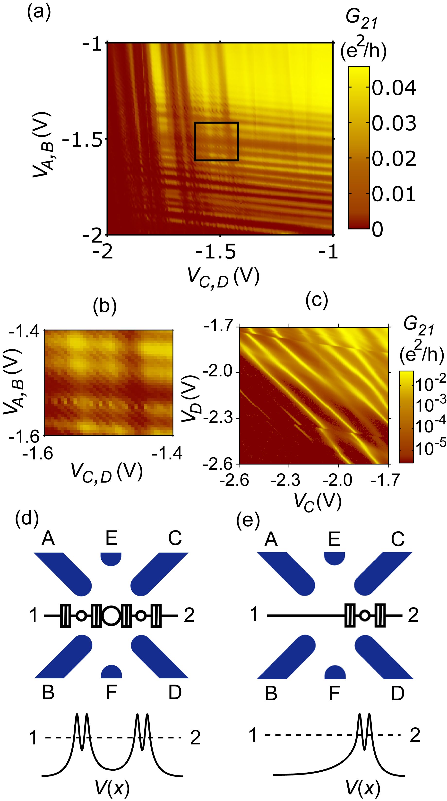
To verify the formation of the quantum dots and to better understand the operation of the device, we have investigated the dependence of the source-drain conductance on and . The observed transfer characteristic shown in Fig. 2(a), a portion of which is enlarged and shown in Fig. 2(b), demonstrates a double quantum dot behavior. When and are both less than about V, the device is in the weakly coupled double quantum dot regime. In this weakly coupled regime, two triple points will merge into ones, i.e. the high conductance spots as clearly shown in Fig. 2(b), and are located at the vertices of parallelograms.van der Wiel et al. (2003) However, when V 1 V, sweeping reproduces the single electron tunneling features similar to that shown in Fig. 1(d). The same is observed when sweeping while keeping V V. The nearly horizontal and vertical lines in Fig. 2(a) indicate that these two dots are spatially separated. One dot is strongly capacitively coupled to side gates A and B, but only weakly coupled to gates C and D. The other, however, is strongly coupled to gates C and D, and only weakly coupled to gates A and B. That is, one dot is physically near side gates A and B, whereas the other dot is located close to side gates C and D. Furthermore, data shown in Fig. 2(c) suggest that the quantum dot is located in the narrow point contact channel. Keeping the other two point contacts fully conductive ( V, V, and V) and sweeping the voltage of side gates C and D in the range of interest, the source-drain conductance shows clear single electron tunneling characteristics. Because the capacitances between the dot and, separately, side gates C and D are the same, the peak positions in Fig. 2(c) display diagonal dependence.van der Wiel et al. (2003) To be more specific, the quantum dot is physically located in the point contact channel, at equal distances to side gates C and D. The discontinuity of the diagonal lines is caused by a mere one electron charge change at a nearby charge trap. Our experiment shows that this nearby charge trap has a negligible effect on our results in this paper. A similar characteristic is also observed for the dot defined by side gates A and B. (Data not shown here.) These observations are consistent with the picture that there are two weakly-coupled quantum dots, located in the point contact channels defined by side gates A, B, and C, D, respectively. Residue interface charges are known to form potential fluctuation at the Si/SiO2 interface.Kastner (1992) It has been reported earlier that a point contact channel in silicon, due to these interface charges, can show Coulomb blockade oscillations.Kastner (1992); Ishikuro and Hiramoto (1997); Lin et al. (2007) In addition to the two quantum dots discussed above, side gates A, B, C, D, E, and F, can also be biased to form a (large) quantum dot. A closer look at Fig. 2(a) indeed reveals the underlining diagonal lines from this dot, as shown in Fig. 2(b).
In summary, under proper bias condition, V and V, the equivalent circuit consists of an SET at the center (with a large quantum dot), in series with two others (both with small quantum dots), as illustrated in Fig. 2(d); on the other hand, a pair of side gates can define a single SET, when the other side gates are positively biased, as shown in Fig. 2(e). These pictures do capture the major characteristics of the device. However, there is not always a quantum dot in a point contact. When the gap between two neighboring side gates is reduced from nm to nm, the point contacts can smoothly turn off the device without Coulomb oscillations in some of our samples. In these devices, the electrostatically defined dot is the only feature, but they currently only work in the many-electron regime. With continuous down-scaling and improvement, it is quite possible to reach the few-electron regime, even realize single electron confinement.
III SINGLE QUANTUM DOT AND MAGNETIC FIELD SPECTROSCOPY
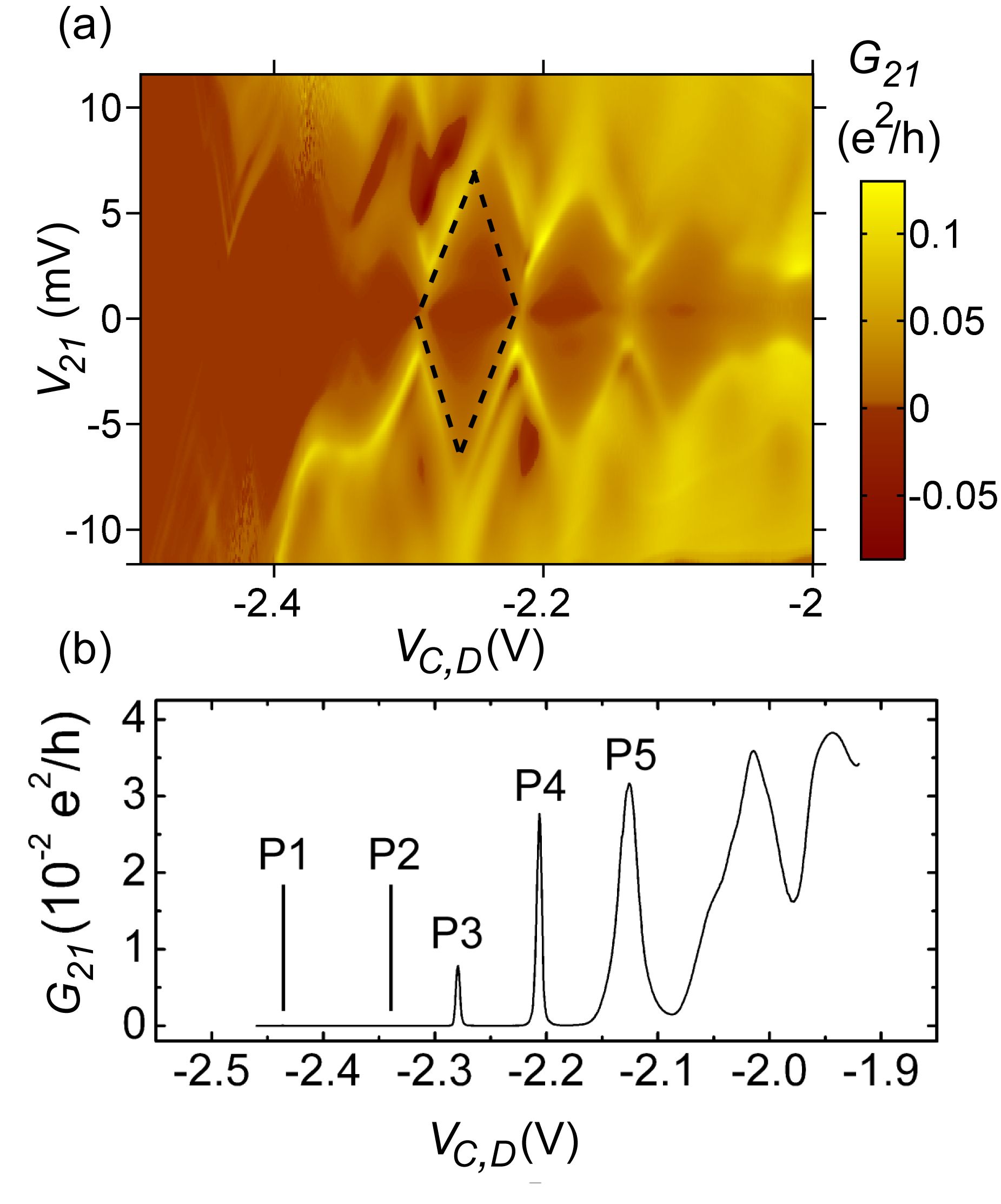
In the following, for the purpose of investigating single spin in silicon, we focus on the single dot SET confined in the channel defined by side gates C and D. Fig. 3(a) shows the stability chart of the SET, where the source-drain differential conductance is measured against the source-drain dc bias, , and the side gate voltages , while V and V. The observation of Coulomb diamonds confirms the formation of a single quantum dot in the point contact channel. Within the orthodox theory, the quantum dot is modeled by a disc with a diameter , and the total capacitance is , where ( in silicon) is the dielectric constant. From the diamond shown in Fig. 3(a), we can directly measure the half height (), and the obtained charging energy () is about 6 meV. So is approximately 27 aF, which suggests a disc diameter of about 60 nm. This estimated disc diameter is of the same order of magnitude as the averaged spacing between the interface-trapped charges in our device; we have separately measured by the conductance method using large area devices the interface quality, and obtained, at room temperature, an interface trap density of eV-1cm-2, corresponding to a spacing between charges to be nm. The origin of the quantum dot of interest is probably coming from negatively charged electron traps, located at the Si/SiO2 interface. Single dopants such as phosphorous atoms had been proposed to be behind transport studiesSellier et al. (2006) in silicon SETs, but our observed addition energy and the excitation energy are both much less than what one would expect using the single dopants picture. In addition, as will be discussed below, we have observed a spin filling pattern different from that of the single phosphorous dopants picture. Other authors proposed that the quantum dots are from Si nanoparticles in their point contact silicon-on-insulator (SOI) devices.Ishikuro and Hiramoto (1997) Our device is free of nanoparticles, thus different from them. Therefore, it is most likely that in our system the negative interface trapped charges create potential barriers along the one-dimensional (1D) point contact channel and form a quantum dot.Kastner (1992) These trapped charges are always present in the Si/SiO2, and the current industrial standard provides an interface trap density of approximately cm-2. In all of the four SETs we have characterized, the single electron tunneling characteristics are similar, although the details of which are sensitive to the specific interface charge distribution. There are changes due to thermal cycling, but the main features discussed here are stable and can be reproduced. Because the top gate threshold voltage is measured to be V for the SET, using a parallel capacitor model and that the quantum disc has a diameter of 60 nm, at V the number of electrons in the quantum dot is estimated to be at most . As the source-drain dc bias is fixed at 0 V, the SET displays the Coulomb blockade oscillations, as shown in Fig. 3(b). The following discussion will be focused on the magnetic field dependence of the first five peaks labeled as P1–P5 in Fig. 3(b).
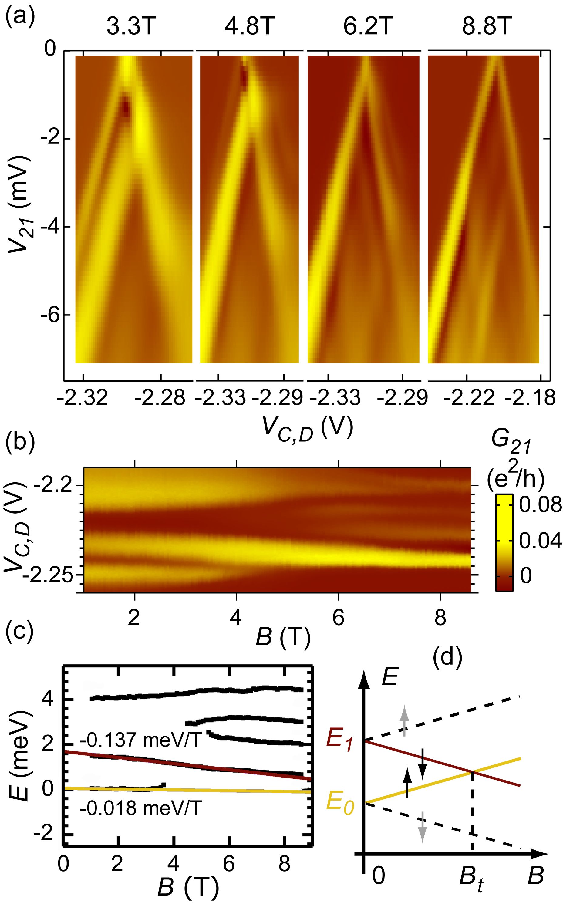
We first focus on the evolution of the ground state and the excited states near peak 4 in magnetic field. The measured excitation spectrum is shown in Fig. 4(b).Kouwenhoven et al. (2001) In Fig. 3(a), there is an excited state near peak 4 ( is about V). Figure 4(a) shows that this excited state moves toward the ground state as the magnetic field increases. When the source-drain dc bias is fixed at mV, and the magnetic field and are swept, the excitation stripe near peak 4 is shown in Fig. 4(b). With the increase of magnetic field ( T), the distance between the first excited state and the ground state decreases. As T, the state becomes the new ground state. The maxima in Fig. 4(b) are fitted with Gaussians (as functions of ), and can be converted into chemical potential, using , where , as defined in Eq. (1).Kouwenhoven et al. (2001) After an arbitrary offset, the resulting peak positions (in chemical potential) are shown in Fig. 4(c). The absolute energy position of a peak in the excitation spectrum is determined by practical experimental parameters; we therefore focus on the difference between the most important features, that is, the energy difference between the “ground state” and the “first excited state” . To first order, both and show apparent linear dependence on magnetic field . We therefore fit (in the range 1 T T) and (in the range 1 T T) by linear lines. Straight lines for the guidance of the eye are shown in Fig. 4(c). The energy difference, , ((meV/T)), is meV/T. The Zeeman splitting in bulk silicon is 0.116 meV/T (, with , is the Bohr magneton.). It is clear that the energy difference is dominated by the Zeeman effect. Figure 4(d) illustrates the Zeeman effect and the ST transition, where we only consider the two electrons in the outmost shell. The lower lying electrons, if any, are ignored, for they do not influence the spin dynamics. For a one-electron system, the ground state is a spin-down state in a magnetic field. The Zeeman splitting has the linear magnetic field dependence, . In Fig. 4(d), the spin of the second electron is depicted by solid black arrows. When this second electron is added to the quantum dot, it would interact with the electron already in the dot and form either singlet or triplet states. As shown in Fig. 4(d), quantum selection rule dictates the spin of incoming electrons, that is, a spin-up state for the singlet state , and a spin-down state for the triplet state . At low magnetic fields, , the singlet state has a lower energy than that of the triplet state. While at a higher magnetic field (), the triplet state becomes the ground state. The spin configuration of the ground states of the two-electron system is therefore controlled by the magnetic field. Were the Zeeman splitting the only effect to be considered, the magnetic field induced ST transition should occur at about 14 T. This estimate is based on the data shown in Fig. 4(c), and that there is meV energy difference between and at zero field. When the size of the electron wave functions shrinks for increasing magnetic field , the interdependence of Coulomb interaction and single-particle states becomes important. Here we only consider the first-order corrections due to the electron-electron interaction in this two-electron system. The chemical potential is for the singlet state, where is the direct Coulomb interaction when both electrons are in the gound state, , and . For the triplet state, the chemical potential is , where and are the direct Coulomb interaction and the exchange interaction respectively when one electron occupies the ground state and the other occupies the first excited state, , and .Kouwenhoven et al. (2001) Both the direct Coulomb interactions and the exchange interaction increase with increasing , since the size of the wave functions decreases. For the triplet state, we hypothesize that is largely compensated by , due to the apparent linear -dependence of the triplet state; while the singlet chemical potential increases with increasing B. So the electron-electron Coulomb interaction (including the direct Coulomb interaction and the exchange interaction) plays a significant role here and drives the singlet-triplet transition at a much lower magnetic field between 4 and 6 T. There are some minor deviations from the linear -dependence of the triplet state, which could be from other effects in addition to this simplified picture. A detailed analysis requires the precise information of the electrostatic potential in the quantum dot, which is beyond the scope of this paper. The conductance of the singlet state drops when T, and it becomes invisible after the ST transition. This is due to the transport blockade effect, which will be discussed later.
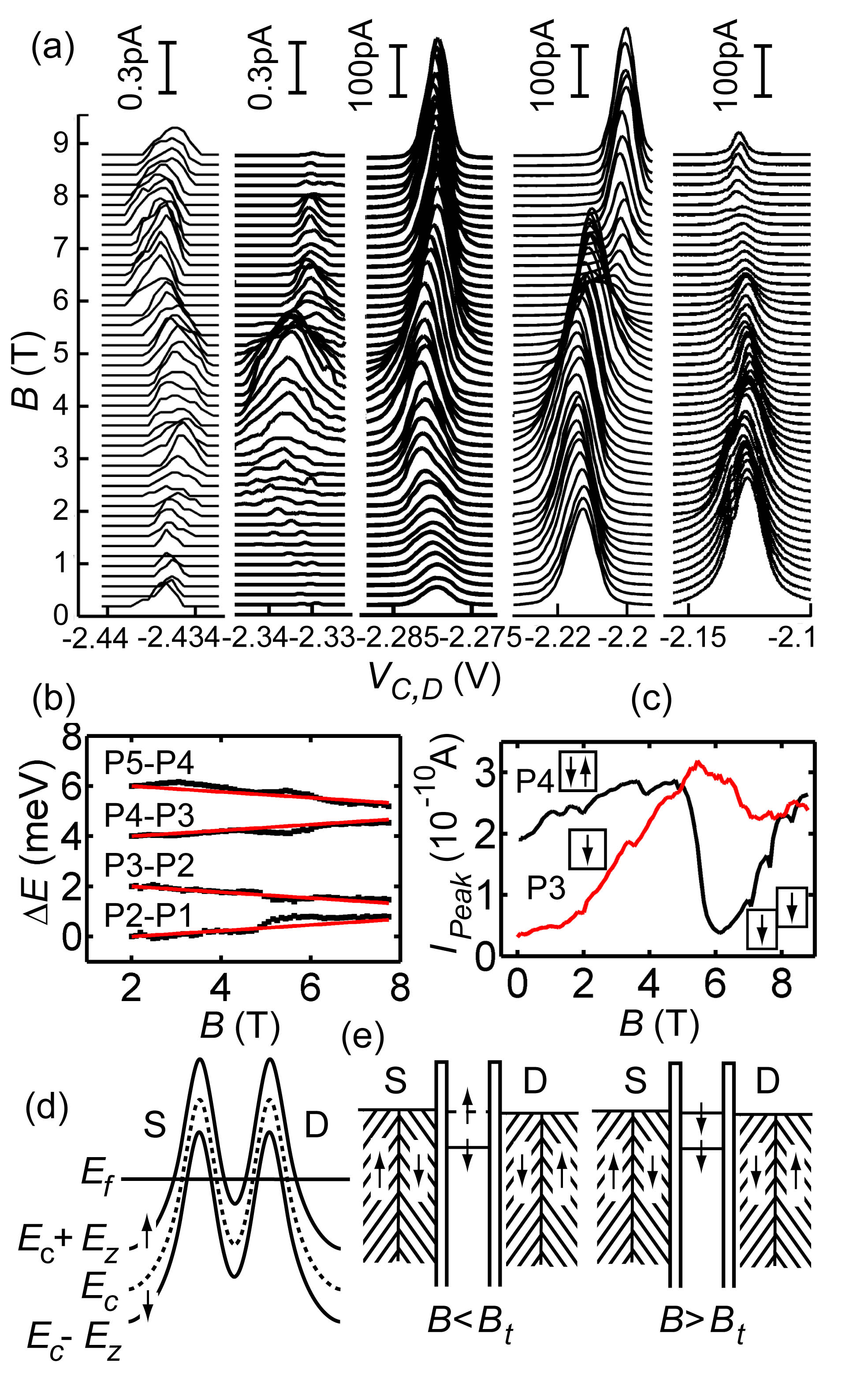
The magnetic field dependence of the first five Coulomb blockade peaks is shown in Fig. 5(a). The peak position and the peak amplitude are extracted from this raw data by fitting each peak with Eq. (1). The shift of peak positions (in ) can be converted into the change in chemical potential using the formula:. In the stability chart [Fig. 3(a)], from the slopes of Coulomb diamonds, is about 0.15, 0.088, 0.090, 0.090 and 0.061 for peaks 1 to 5, respectively.Kouwenhoven et al. (2001) These changes in chemical potential reflect the evolution of the ground state energies. Figure 5(b) shows the peak spacing (in chemical potential) between successive peaks as a function of magnetic field. Using the energy difference in our analysis not only minimizes the uncertainty due to charge fluctuation and the long term drift in analog electronics, but also helps in identifying the role of spin in the addition energy spectrum. Based on the Zeeman splitting, four straight lines with slopes of either or , with g=2, are plotted. Since the second peak only appears between 2 T and 8 T, we compare the first 5 peaks in this field range. Each curve is arbitrarily offset for clarity. Because the chemical potential differences between successive peaks show the alternate slopes of and , it is clear that the shifts of the ground states show an spin-down spin-up filling pattern and are dominated by the Zeeman effect at low magnetic field ( T). Note that such odd-even-odd-even alternate filling pattern is different from that due to isolated single dopants in silicon.Sellier et al. (2006) The fact that the data are well explained by the Zeeman splitting is consistent with our earlier finding that the magnetic field dependence of energy levels (both the ground state and the excited state) is primarily driven by the Zeeman effect. For the data reported in this work, the magnetic field is applied perpendicular to the sample surface, therefore, the orbital effect might be expected. However, all of the observed magnetic field dependence can be well explained by the Zeeman effect with a g-factor of , leaving orbital effect not a significant factor in our system. This is caused by the specific shape of our quantum dot. When we squeeze side gates C and D, the electron wave function is elongated along the source-drain direction, the orbital effect becomes negligible. This leaves the dependence of the peak positions dominated by spin effects.Rokhinson et al. (2001)
The SET is fabricated on a Si (100) wafer, so the valley splitting from the two-fold valley degeneracy is expected. It is generally believed in a Si (100) inversion layer that the valley splitting ranges from meV, increases with increasing electric field or magnetic field, and also depends on the Si/barrier interface.Ando et al. (1982); Goswami et al. (2007) But detailed relationships between them are not clear yet. The valley splitting in Si quantum dots has not been systematically investigated in experiments, primarily due to the lack of the excitation spectrum data. Some speculate that it is meV.Goswami et al. (2007) Others indicate that it is of order of a few meV and greater even at T.Takashina et al. (2006); Liu et al. (2008) In our SET, the spin-down spin-up filling pattern requires that the valley degeneracy is lifted,Rokhinson et al. (2001) and the excitation spectrum suggests that the valley splitting should be larger than 1.6 meV. This is probably due to the strong lateral confinement in our quantum dot. Further investigation is necessary to reach an affirmative conclusion.
Finally, we turn our attention to the tunneling peak amplitudes in Fig. 5(a). In a lateral quantum dot device, an electron tunnels into and out of the quantum dot from the two-dimensional electron gas (2DEG) leads. As illustrated in Fig. 5(d), the electron concentration will vary from the bulk value to zero near the tunneling barriers; the Zeeman splitting effect will cause the separation of the conduction band minima of the spin-up and spin-down electrons in a magnetic field, which will result in the different populations of the spin-up and spin-down subbands. In GaAs, spin polarized injection is due to edge states in a magnetic field perpendicular to the 2DEG.Ciorga et al. (2000) This edge-state picture is probably not valid in our silicon devices, because the Shubnikov-de Hass oscillation minima are not zero up to 9 T in the test hall bar device. However, magnetic field can fully spin polarize a 2DEG with cm-2 for T solely with spin effects in a high mobility Si MOSFET.Vitkalov et al. (2001); Shashkin et al. (2001) In the test hall bar device, the Shubnikov-de Hass oscillations show that the 2DEG is spin polarized at least at T for cm-2. So it is reasonable to expect that electrons will be polarized into the spin-down state in the 2DEG leads near the tunneling barriers above some magnetic field, as illustrated in Fig. 5(d). This effectively makes the spin-up electrons tunnel through a thicker barrier, so the injection is dominated by spin-down electrons.
In theory, peak amplitude is proportional to the tunneling probability and depends exponentially on how much wave functions in the dot and in the contacts overlap with each other.Rokhinson et al. (2001) There are two different mechanisms governing the amplitude modulation of Coulomb blockade peaks in a magnetic field. One is the spatial mechanism when an electron tunnels into different spatial wave functions in a quantum dot, not related to spin; the other is the spin-blockade mechanism due to spin-polarized injection.Sachrajda et al. (2001) The lower edge of the excitation stripe in Fig. 4(b) reflects the evolution of peak 4 as a function of magnetic field in Fig. 5(a). The conductance of the singlet state drops dramatically when T, while the conductance of the triplet state doesn’t change much, as shown in Fig. 4(b) and Fig. 5(a). This difference can be explained by both the spatial effect and the spin-blockade effect, since the singlet state requires a spin-up electron which occupies a smaller wave function at the center, while the triplet state requires a spin-down electron which occupies a larger wave function. However, the electron states corresponding to peak 3 (a spin-down single electron state) and peak 4 (a singlet state) should have similar (single-particle) spatial wave functions; their peak amplitude should have similar dependence on the magnetic field if there is no spin blockade effect. In Fig. 5(c), the amplitude of peak 4 decreases much faster than peak 3 when the magnetic field is larger than 4 T. A reasonable explanation is the spin polarized injection from the leads.Sachrajda et al. (2001) For 0.1 mV small ac excitation between the source and the drain, only ground states can lie in the transport window. For a singlet state, only a spin-up electron can tunnel into and out of the quantum dot, the amplitude of peak 4 decreases dramatically owing to this spin polarized injection, and as shown in Fig. 5(c), it occurs at T. This forms the spin blockade. After T, the amplitude of peak 4 increases with the magnetic field, because the ground state corresponding to peak 4 changes from a singlet state to a triplet state. For the triplet state, the incoming spin-down electron experiences lower and thinner barriers, thus the higher conductance. Since the amplitude of Coulomb blockade peaks is determined by the two-electron spin configuration in the dot with spin polarized leads, it can be used to distinguish a singlet state from a triplet one. Monitoring the amplitude is thus a form of spin blockade spectroscopy.Ciorga et al. (2000)
IV CONCLUSIONS
We have investigated electron spin in a nanometer-scale quantum dot in silicon. Using the unique bilayer-gated structure, narrow point contact channels are electrostatically defined. Along the narrow channel, a quantum dot is formed by potential barriers, probably due to negative charges near the Si/SiO2 interface. Tunneling spectroscopy clearly demonstrates the single electron tunneling characteristics. There are two important spin-related features. First, applying excitation spectroscopy on a dot populated by even number of electrons, we have directly observed the ST transition. Second, based on the observed ST transition, we further use amplitude spectroscopy, i.e., tracing the magnetic field dependence of Coulomb blockade peaks, to identify the spin blockade phenomena. With a spin polarized injection, we demonstrate that the amplitude spectroscopy can be used to detect a single spin.
Acknowledgements.
This work is supported in part by the Laboratory for Physical Sciences and the Office of Naval Research. The authors are grateful to Bruce Kane, Luyan Sun, Tomasz Kott, and Greg Jones, for insightful discussions and technical help. The authors also acknowledge the Laboratory for Physical Sciences for the use of their fabrication facilities.References
- Loss and DiVincenzo (1998) D. Loss and D. P. DiVincenzo, Phys. Rev. A 57, 120 (1998).
- Koppens et al. (2006) F. H. L. Koppens, C. Buizert, K. J. Tielrooij, I. T. Vink, K. C. Nowack, T. Meunier, L. P. Kouwenhoven, and L. M. K. Vandersypen, Nature (London) 442, 766 (2006).
- Petta et al. (2005) J. R. Petta, A. C. Johnson, J. M. Taylor, E. A. Laird, A. Yacoby, M. D. Lukin, C. M. Marcus, M. P. Hanson, and A. C. Gossard, Science 309, 2180 (2005).
- Feher (1959) G. Feher, Phys. Rev. 114, 1219 (1959); A. M. Tyryshkin, S. A. Lyon, A. V. Astashkin, and A. M. Raitsimring, Phys. Rev. B 68, 193207 (2003).
- Fujiwara et al. (2006) A. Fujiwara, H. Inokawa, K. Yamazaki, H. Namatsu, Y. Takahashi, N. M. Zimmerman, and S. B. Martin, Appl. Phys. Lett. 88, 053121 (2006).
- Simmons et al. (2007) C. B. Simmons, M. Thalakulam, N. Shaji, L. J. Klein, H. Qin, R. H. Blick, D. E. Savage, M. G. Lagally, S. N. Coppersmith, and M. A. Eriksson, Appl. Phys. Lett. 91, 213103 (2007).
- Jones et al. (2006) G. M. Jones, B. H. Hu, C. H. Yang, M. J. Yang, R. Hajdaj, and G. Hehein, Appl. Phys. Lett. 89, 073106 (2006).
- Angus et al. (2007) S. J. Angus, A. J. Ferguson, A. S. Dzurak, and R. G. Clark, Nano. Lett. 7, 2051 (2007).
- Kouwenhoven et al. (2001) L. P. Kouwenhoven, D. G. Austing, and S. Tarucha, Rep. Prog. Phys. 64, 701 (2001).
- Beenakker (1991) C. W. J. Beenakker, Phys. Rev. B 44, 1646 (1991).
- van der Wiel et al. (2003) W. G. van der Wiel, S. D. Franceschi, J. M. Elzerman, T. Fujisawa, S. Tarucha, and L. P. Kouwenhoven, Rev. Mod. Phys. 75, 1 (2003).
- Kastner (1992) M. A. Kastner, Rev. Mod. Phys. 64, 849 (1992).
- Ishikuro and Hiramoto (1997) H. Ishikuro and T. Hiramoto, Appl. Phys. Lett. 71, 3691 (1997).
- Lin et al. (2007) M. C. Lin, K. Aravind, C. S. Wu, Y. P. Wu, C. H. Kuan, W. Kuo, and C. D. Chen, Appl. Phys. Lett. 90, 032106 (2007).
- Sellier et al. (2006) H. Sellier, G. P. Lansbergen, J. Caro, S. Rogge, N. Collaert, I. Ferain, M. Jurczak, and S. Biesemans, Phys. Rev. Lett. 97, 206805 (2006).
- Rokhinson et al. (2001) L. P. Rokhinson, L. J. Guo, S. Y. Chou, and D. C. Tsui, Phys. Rev. B 63, 035321 (2001).
- Ando et al. (1982) T. Ando, A. B. Fowler, and F. Stern, Rev. Mod. Phys. 54, 437 (1982).
- Goswami et al. (2007) S. Goswami, K. A. Slinker, M. Friesen, L. M. McGuire, J. L. Truitt, C. Tahan, L. J. Klein, J. O. Chu, P. M. Mooney, D. W. van der Weide, et al., Nature Physics 3, 41 (2007).
- Takashina et al. (2006) K. Takashina, Y. Ono, A. Fujiwara, Y. Takahashi, and Y. Hirayama, Phys. Rev. Lett. 96, 236801 (2006).
- Liu et al. (2008) H. W. Liu, T. Fujisawa, Y. Ono, H. Inokawa, A. Fujiwara, K. Takashina, and Y. Hirayama, Phys. Rev. B 77, 073310 (2008).
- Ciorga et al. (2000) M. Ciorga, A. S. Sachrajda, P. Hawrylaka, C. Gould, P. Zawadzki, S. Jullian, Y. Feng, and Z. Wasilewski, Phys. Rev. B 61, 16315 (2000).
- Vitkalov et al. (2001) S. A. Vitkalov, M. P. Sarachik, and T. M. Klapwijk, Phys. Rev. B 64, 073101 (2001).
- Shashkin et al. (2001) A. A. Shashkin, S. V. Kravchenko, V. T. Dolgopolov, and T. M. Klapwijk, Phys. Rev. Lett. 87, 086801 (2001).
- Sachrajda et al. (2001) A. S. Sachrajda, P. Hawrylaka, M. Ciorga, C. Gould, and P. Zawadzki, Physica E 10, 493 (2001).