The TRB for HADES and FAIR experiments at GSI111 Proceedings of the 10th Conference on Astroparticle, Particle and Space Physics, Detectors and Medical Physics Applications, 973-977, 2008
I. FRÖHLICH, J. MICHEL, C. SCHRADER, H. STRÖBELE, J. STROTH, A.TARANTOLA
Institut für Kernphysik, Goethe-Universität,
60486 Frankfurt, Germany
M. KAJETANOWICZ
Nowoczesna Elektronika
Pl-30-109 Cracow, Poland
K. KORCYL, W. KRZEMIEN∗, M. PALKA, P. SALABURA, R. TREBACZ
Institute of Physics, Jagiellonian University,
Pl-30-059 Cracow, Poland
∗E-mail: wojciech.krzemien@if.uj.edu.pl
P. SKOTT, M. TRAXLER
GSI
Helmholtzzentrum für Schwerionenforschung GmbH
64291 Darmstadt, Germany
Abstract
The TRB hardware module is a multi-purpose Trigger and Readout Board with on-board DAQ functionality developed for the upgrade of the HADES experiment. It contains a single computer chip (Etrax) running Linux as a well as a 100 Mbit/s Ethernet interface. It has been orginally designed to work as a 128-channel Time to Digital Converter based on the HPTDC chip from CERN. The new version contains a 2 Gbit/s optical link and an interface connector (15 Gbit/s) in order to realize an add-on card concept which makes the hardware very flexible. Moreover, an FPGA chip (Xilinx, Virtex 4 LX 40) and a TigerSharc DSP provide new computing resources which can be used to run on-line analysis algorithms. The TRB is proposed as a prototype for new modules for the planned detector systems PANDA and CBM at the future FAIR facility at GSI-Darmstadt.
Keywords: Triggering; Data acquisition.
1 Introduction
HADES is a high resolution dilepton spectrometer for hadron and heavy ion physics at the SIS18 accelerator facility of GSI, Germany [1]. Its main goal is the study of in-medium modification of light vector mesons properties. PANDA [2] and CBM [3] are detector systems which will operate at the new Facility of Antiproton and Ion Research (FAIR) at GSI. The large research program of PANDA and CBM will address the questions of the generation of mass, spontaneous breaking of chiral symmetry, the limits of hadronic existence and the transition to de-confined matter [4]. To provide access to rare decay channels the experiments will be operated at high luminosity. The cross sections and branching ratios of interesting processes are low and the background will be of orders of magnitude higher in yields. Therefore, to collect statistically relevant data, the detector systems should operate with interaction rates above 10 MHz, which is a real challenge for the data acquisition systems. HADES has worked out a two-level trigger system whereas PANDA and CBM plan to design their DAQ systems without any central trigger. Thus, data generated by the PANDA and CBM subdetectors will be time stamped and sent to the event buildind system. In all detector systems mentioned above, a large amount of data has to be handled which calls for high level data reduction mechanisms. In this context, a universal readout electronics for various detectors has been developed. The “Trigger and Readout Board” (TRB) is a general-purpose electronic device which can be used as base readout module for the development of the future DAQ systems in the FAIR experiments.
2 The TRB version 1
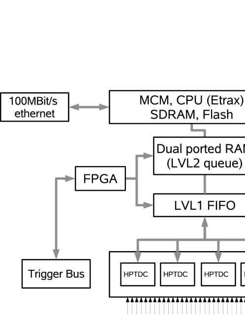
TRB version 1 (TRBv1) has been orginally developed as a 128-channel Time to Digital Converter based on the HPTDC [6] chips.

It contains 4-input connectors (high density 80 pins). Each connector permits to sample 31 LVDS timing signals. Four 32-channel HPTDC chips perform time to digital conversion. The 32th channel of each HPTDC is connected to the external reference timing signal. The HPTDC chips are highly configurable [6]. The TDC binnig could be chosen in the range of 25 to 780 ps. The HPTDC allows to measure rising and falling edges, and to define a matching window. Moreover, the TRBv1 contains an FPGA (Xilinx Spartan 2), a FIFO queue and dual ported RAM memory. The slow control and the readout functionality (for HADES) is done via an Etrax single chip computer running the Linux operation system [7]. The data acquisition is started by an external level one trigger (LVL1). The FPGA controller initiates the readout and selected data from HPTDC is stored in the FIFO queue upon the level two trigger (LVL2) has been received. If the LVL2 signal is positive data is moved to the dual ported RAM. The data is consequently read out by the Etrax and send via UDP protocol over 100 Mbit/s Ethernet to the event builder.
The time resolution between two channels from different HPTDC chips resulted 40 ps (with 100 ps binning) [5]. The crosstalk influence to resolution has been estimated to be less than 20 ps. The maximum data transport rate via UDP has been measured to be 8 MB/s [7]. The maximum LVL2 trigger rate was about 18 kHz. The TRBv1 has been tested and succesfully used in the new RPC detector as a part of the upgrade of HADES detector system.
3 TRB board version 2
The enhanced version of TRB module (TRBv2) has been developed. The TRBv2 has been designed as a multi-purpose readout module which could be used for all types of detectors.

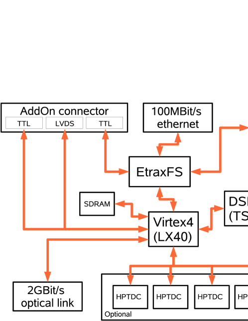
It uses an Etrax-FS processor running Linux for DAQ and slow-control functionality. It has three integrated I/O co-processors (each 200 MHz) which allow to use the bandwidth more efficentally without using too much CPU computing resources, thus eliminating the bottelneck observed in the TRBv1. The TRBv2 has in addition an optical link 2 Gbit/s which can be used for data transmission in the future applications (e.g. PANDA and CBM). The FPGA in the TRBv2 has been upgraded to a Xilinx Virtex 4 LX40 with 128 MB RAM. Moreover, the new version provied an optional TigerSharc DSP which may be used to implement on-line analysis algorithms. To broaden the spectrum of the applications, the TRBv2 is equipped with a high data-rate digital interface connector (32 LVDS lines, 15 GBit/s) which allows to connect add-on boards with the TRB. The concept of add-on boards is explained in the next section.
4 Add-on cards
The TRBv2 has been designed as a detector-independent readout module. All detector-specific FEE, interfaces and connectors are placed on the add-on cards which can be easily mounted on the TRB. Additional computing resources such as FPGA or DSP could be added to the add-on card. The first add-on card for the HADES-MDC (“Multiwire Drift Chambers”) readout has been developed [9]. It has 10 connectors. Each connector has 50 pins and two RS485 transcivers. The operation of the MDC-add-on card is controlled by the FPGA (Xilinx, XC4VLX-10FF1148) chip. The MDC-add-on board is connected back to back to the TRBv2 via two connectors (SAMTEC QSE-040-01, 80 pins each) and allows to read out each MDC-chamber by one single TRB board. The concept of add-on boards provides a possibility to mount specific-detector resources in a flexible way, using the same base readout module for each detector.
5 Conclusion
The multi-purpose trigger and readout board with on-board DAQ functionality (TRB) has been presented. The TRB has been designed for the HADES readout system. However, it can be used also in new CBM and PANDA detector systems which will operate at FAIR facility at GSI. The TRB version 1 has been designed as a 128-channel Time to Digital Converter (TDC) based on the HPTDC chip. The module has been successfully implemented to readout the RPC detector. As it has already the TDC chips on-board, it has been also used for the prototype drift chamber readout tests for PANDA. The TRB version 2 has an 2 GBit/s optical link (also very important for PANDA), add-on card connectors, as well as an optional TigerSharc DSP. Add-on boards for MDC, PreShower and for other types of detectors are currently being tested. It is planned to use one more add-on board to serve for the readout the MAPS sensors for the CBM experiment [8]. Thus, the TRB module is proposed as a usefull componant for new FAIR experiments.
Acknowledgments
This work has been supported by the EU under the contracts CNI DIRAC-PHASE-1 (515876) and Hadron Physics (RII3-CT-2004-506078), the BMBF, the Helmholtz Research School, the Polish MEEN (158/E-338/SPB/6.PR UE/DIE 455/2004-2007) and GSI.
References
- [1] High Acceptance Dilepton Spectrometer, http://www-hades.gsi.de/
- [2] M. Kotulla et al. [PANDA Collaboration], “Strong interaction studies with antiprotons. Letter of intent for PANDA (Antiproton Annihilations at Darmstadt)”.
- [3] P. Senger, T. Galatyuk, D. Kresan, A. Kiseleva and E. Kryshen, “CBM At FAIR,” PoS CPOD2006, 018 (2006).
- [4] J. Stroth, “The Future At GSI And FAIR”, Nucl. Phys. A 755, 209 (2005).
- [5] I. Fröhlich et al., “A General Purpose Trigger and Readout Board for HADES and FAIR-Experiments”, IEEE Trans. Nucl. Sci. 55, 59 (2008).
- [6] J. Christiansen, Digital Microelectronics Group, CERN.
- [7] R. Trebacz, “Single-Chip-Linux-Computer for the HADES-experiment Data-Acquisition”, GSI Summer Student Programm 2004.
- [8] C. Schrader el al., “A Readout System for the CBM-MVD Demonstrator”, GSI Scientific Report 2007.
- [9] A. Tarantola el al., “The Upgrade of the Multiwire Drift Chamber Readout of the HADES Experiment at GSI.”, XLVI International Winter Meeting on Nuclear Physics.