Measurements of Charge Transfer Inefficiency in
a CCD with High-Speed Column Parallel Readout
André Sopczak1,
Khaled Bekhouche1,
Chris Damerell2,
Tim Greenshaw3,
Michal Koziel1,
Konstantin Stefanov2,
Tuomo Tikkanen3,
Tim Woolliscroft3,
Steve Worm2
1Lancaster University, UK
2STFC Rutherford Appleton Laboratory, UK
3Liverpool University, UK
Abstract
Abstract
Charge Coupled Devices (CCDs) have been successfully used in several high energy physics experiments over the past two decades. Their high spatial resolution and thin sensitive layers make them an excellent tool for studying short-lived particles. The Linear Collider Flavour Identification (LCFI) collaboration is developing Column-Parallel CCDs (CPCCDs) for the vertex detector of a future Linear Collider. The CPCCDs can be read out many times faster than standard CCDs, significantly increasing their operating speed. A test stand for measuring the charge transfer inefficiency (CTI) of a prototype CPCCD has been set up. Studies of the CTI have been performed at a range of readout frequencies and operating temperatures.
I Introduction
The study of radiation hardness is crucial for the application of CCD detectors in High Energy Physics experiments [1, 2, 3]. The LCFI collaboration has been developing and testing new CCD detectors for about 10 years [1, 2, 3, 4, 5]. Previous experimental results on CCD radiation hardness were reported for example in [6, 7, 8]. Several models increased the understanding of radiation damage effects in CCDs [9, 10, 11]. The measurements and analyses reported in this paper have been carried out in the LCFI collaboration [3]. Simulation and modelling of CCD radiation hardness effects for a CCD prototype with sequential readout was reported at IEEE’2005 [12], comparing full TCAD simulations with analytic models was reported at IEEE’2006 [13] and in Ref. [14], simulation and modelling of a CCD prototype with column parallel readout (CPCCD) at IEEE’2007 [15] and in Ref. [16].
This work focuses on experimental measurements and a method to determine the charge transfer inefficiency (CTI) performed with the CPCCD at a test stand at Liverpool University.
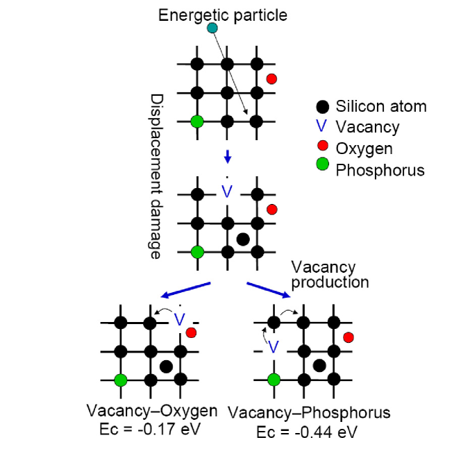
The environment with high radiation near the interaction point at a future Linear Collider creates damage to the CCD material which leads to defects acting as electron traps in the silicon, as indicated in Fig. 1. The mechanism of creating traps has been discussed in the literature, for example in Refs. [17, 18, 19]. These traps result in charge transfer inefficiency. In a phosphorus-doped device, two types of traps are created. The first one is relatively shallow with energy level eV below the conduction band and the second is deep with energy level eV below the conduction band. These traps result in charge transfer inefficiency.
The column parallel technology is in development to cope with the required readout rate. CPC1 is a two-phase CCD prototype capable of MHz readout frequency. In this paper we demonstrate the method to determine the CTI value with an un-irradiated CPCCD (CPC1).
II Test stand for CCD operation and cryostat unit
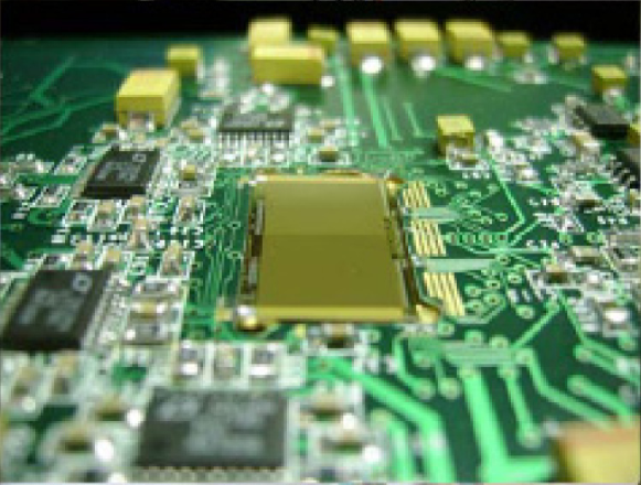
A test stand has been set up with readout electronics and a cryostat unit. The temperature range of the cryostat is from room temperature down to about C. This temperature has been achieved with cold nitrogen gas by boiling liquid nitrogen. The very low operating temperature is required to obtain sensitivity to the CTI peak structure for eV traps where the peak position is expected to be near C [16]. Initial measurements have been performed on an un-irradiated device in standalone mode, where the signal from four columns of the CCD were amplified and connected to external ADCs. An 55Fe source emitting keV X-rays was attached to a holder at a distance of cm from the CCD to provide the signal charge. Figure 2 shows a picture of CPC1 and the associated control and front-end readout electronics, which were also placed in the cryostat, wherefrom the four outputs were fed to rack-mounted amplifiers and ADCs.
It was observed that the CTI increased sharply when the amplitude of the sinusoidal clock pulses applied to read out the CCD was reduced to less than V peak-to-peak. In order to suppress any effect from the clock amplitude, settings for each data acquisition were tuned to produce clock pulses. The performance of the drivers limited the maximum clocking frequency to about MHz. The settings depended on the frequency and had to be adjusted for each cryostat temperature.
III Signal measurement and removing charge sharing by using a 33 cluster method
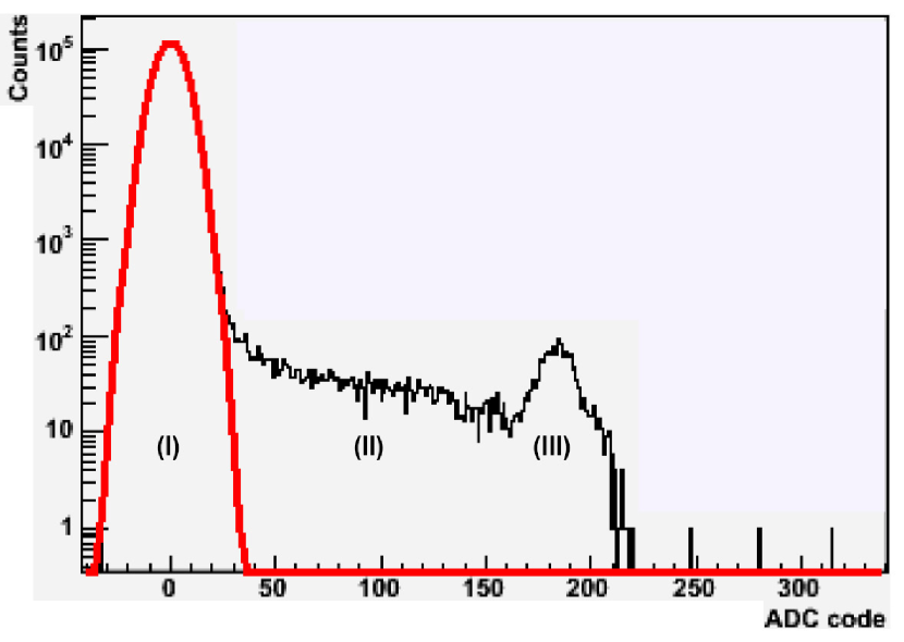
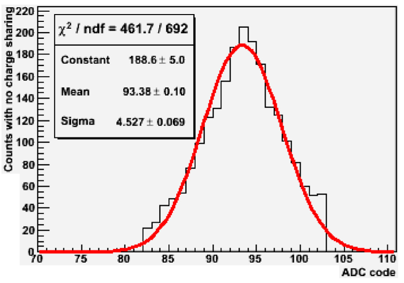
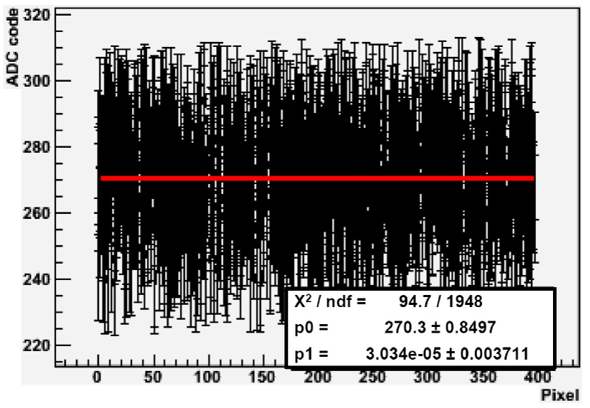
The fast ADCs convert the signal charge after amplification with a wideband preamplifier. The four columns are read out in 4 channels by ADCs. Three columns (channels 1 to 3) are adjacent whereas channel 4 is separate. The signal charges of 400 pixels plus 10 overclocks were acquired in 3000–5000 frames per measurement. This leads to an accurate statistical precision. The collected data has been analysed using the ROOT package [20]. First, we begin by applying correlated double sampling, where the difference between the signals of two consecutive pixels is taken to be the signal charge collected by the latter pixel. This decreases electronic noise. Next, we remove common mode noise components for each column with the help of the overclocks. Overclocks are charges read out after the last pixel of the column. We average all overclocks of a column and subtract the average from the data of all pixels in the column. As an example for channel 2 Fig. 3 shows the distribution of ADC codes for all recorded pixels and all frames of one measurement. The analysis is performed on column 2 because it is situated between columns 1 and 3. This allows to apply a 33 cluster method.
Figure 3 illustrates that there are 3 regions in ADC codes. The first region (I) has a high number of pixels with low ADC codes from electronics noise only (no charge from X-rays). The noise is fitted by a Gaussian function in order to determine the noise threshold. The charge-sharing region (II) represents the signal charge shared between 2 or more pixels. Region (III) is the signal region where the charge is collected in a single pixel that will be analysed to determine the CTI.
In order to remove hits with shared charges, a 33 cluster method is used (Fig. 4). This method is only applied to the 3 adjacent columns (1, 2 and 3). Column 2 is considered, where the signal charge of a pixel is accepted only if no X-ray charge is present in the neighboring pixels.
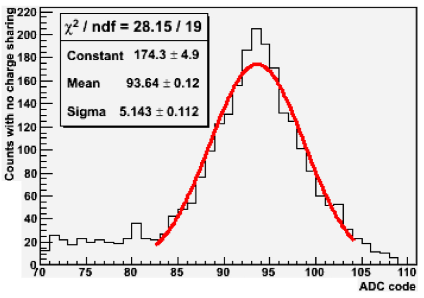
The noise threshold is used to separate noise from shared X-ray charges. It is determined by fitting the noise peak with a Gaussian function. The threshold is usually set to be above the fitted peak centroid. After removal of the noise and reduction of the charge-sharing events, a tail remains for the X-ray peak as shown in Fig. 5. In order to separate the X-ray signal region from the charge-sharing region we exclude all ADC codes below an X-ray threshold which is determined by fitting the X-ray peak. We usually set the threshold to be below the fitted peak centroid but with weaker X-ray peaks the fitted Gaussian sometimes failed to follow the real shape of the peak, and then the limits were set by visual inspection. In this way we obtain the measured X-ray signal data in the pixels with full X-ray charge (Fig. 6).
IV Baseline correction for different operating temperatures and readout frequencies
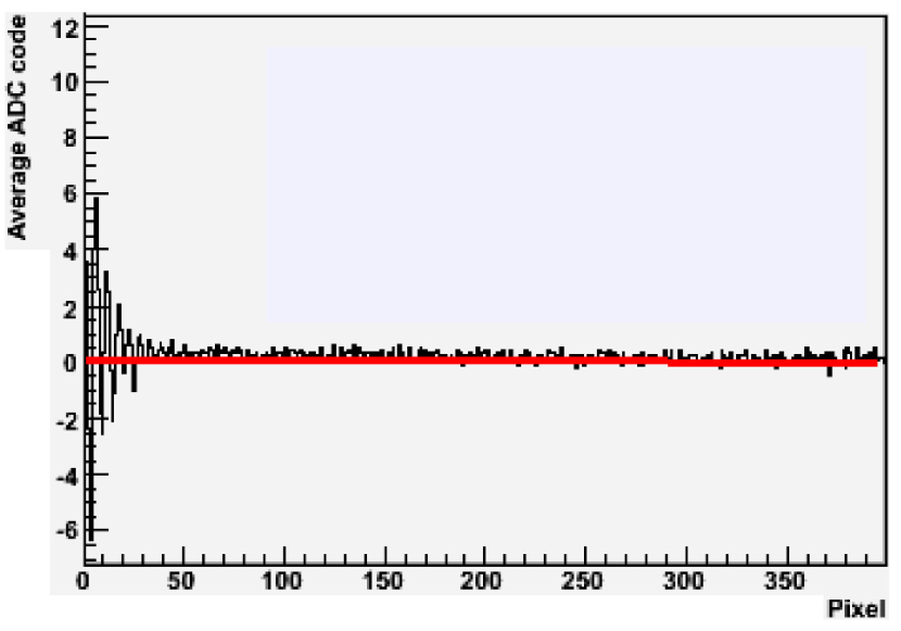
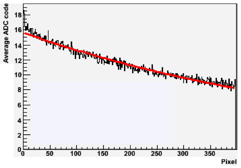
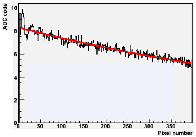
Owing to an RC coupling at the preamplifier input, the output voltage decays exponentially with a time constant equal to ( is of the order of s)111For a readout frequency of MHz reading out the whole column of 400 pixels takes a time comparable to .. This is expected to give rise to an exponential baseline that varies during the clocking sequence, adding a contribution to the readout signal that depends on the pixel number. The shape of the baseline can be determined by comparing the average output level in the pixels to each other. For each pixel an average of the ADC codes was computed excluding the frames were the code exceeded the noise threshold. The average ADC code can usually be expected to be an exponential function of the pixel number with the RC decay. Figures 7, 8, 9 and 10 show the distributions of the average ADC codes for all frames of a measurement as a function of the pixel number for different readout frequencies and operating temperatures. These distributions are fitted by an exponential function given by , where corresponds to the signal charge at the first pixel, is the slope and is the pixel number. This function will be subtracted from the X-ray data. Figures 7 and 10 show approximately zero baseline level, whereas Figs. 8 and 9 show non-zero baseline fits. The baseline level is much smaller at low temperatures, for example at C (Fig. 7) and at C (Fig. 10). Figures 8 and 9 show baselines for higher temperatures C and C, respectively. The observed baselines show different frequency and temperature dependence from what is expected from the RC effect. This indicates that other electronic effects also influence the baseline.
V Determination of Charge Transfer Inefficiency
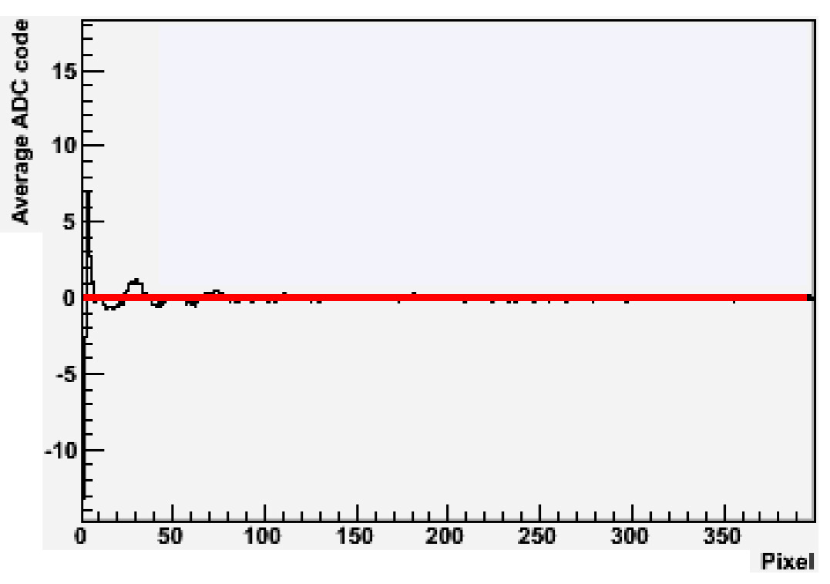
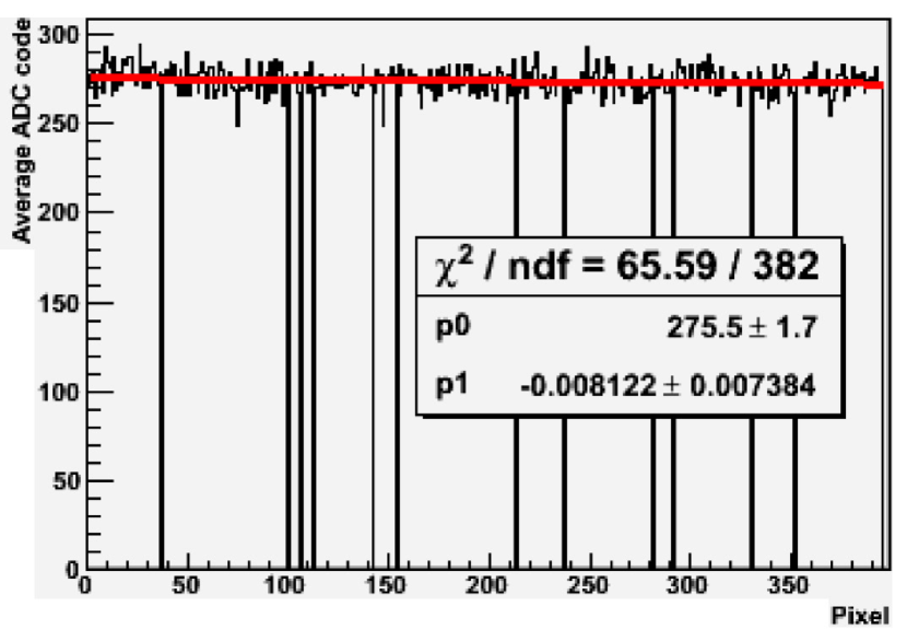
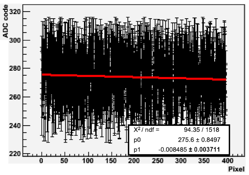
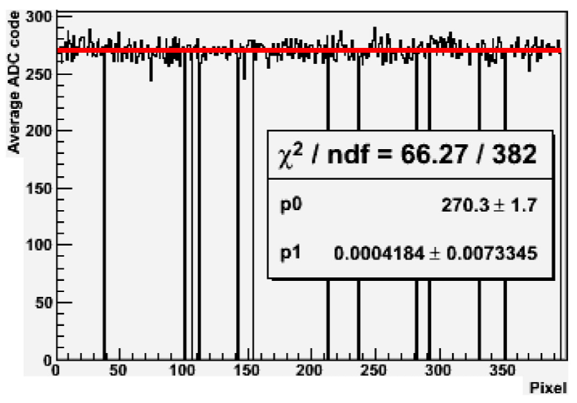
The charge transfer inefficiency (CTI) in one pixel is defined as the ratio of signal lost during transfer (captured by traps) to the initial signal charge. For an un-irradiated CCD we expect that the CTI value is consistent with zero within uncertainties. In order to determine the CTI we first make the overclock correction and apply the cluster method. Then, the X-ray peak was fitted with the Gaussian function to determine the X-ray threshold. This was used to construct the two distributions with a fit of average ADC codes as shown in Fig. 11 and with a fit of individual events (X-ray hits) as shown in Fig. 12. Both distributions are fitted with the first-order polynomial function , where corresponds to the charge at the first pixel, is the slope and is the pixel number. These distributions are plotted without baseline removal. Figures 13 and 14 show the distributions of the averages and all events as a function of pixel number with baseline removal. The CTI is determined for the four cases using
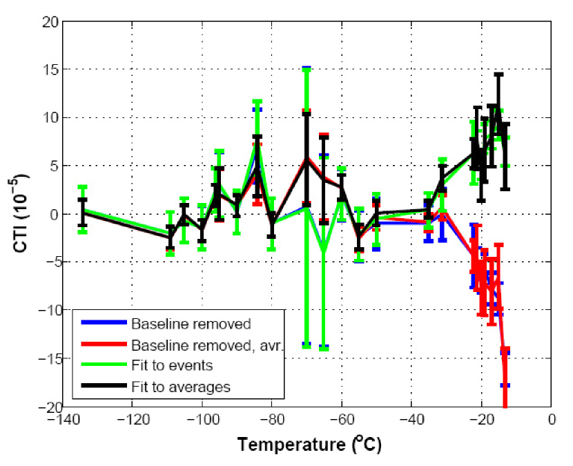
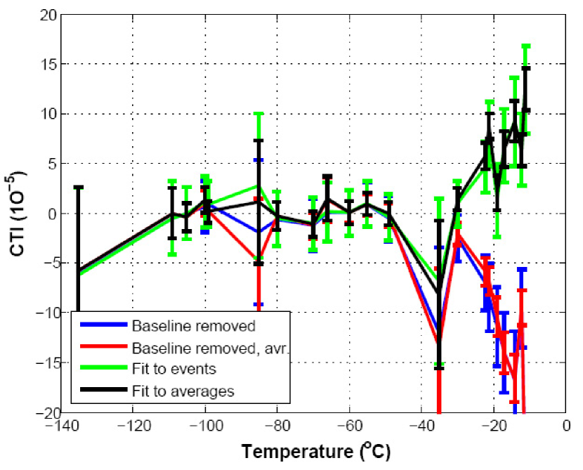
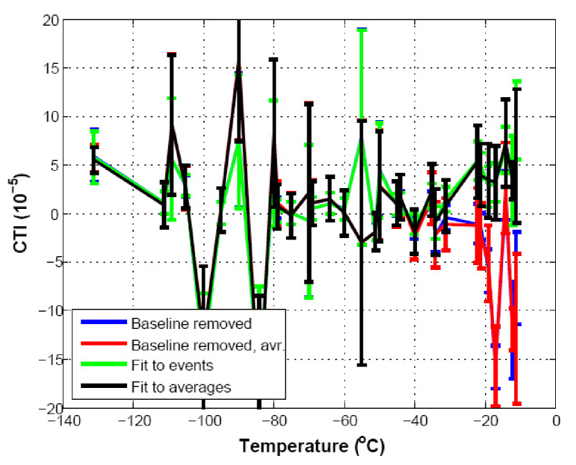
VI CTI results pre-irradiation for different readout frequencies
Figures 15, 16 and 17 show the CTI values as a function of temperature for an un-irradiated CPC1 at different readout frequencies. The CTI has been calculated using two methods, a linear fit of averages versus pixel number and using a linear fit of events (X-ray hits) versus pixel number. As it is expected for an un-irradiated CCD, the CTI is small because the density of traps is small. In the temperature region below C no frequency dependence of the CTI measurements is observed. One may note that in the region of rather high temperatures (above C) the effect of baseline removal is large and the determined CTI values indicate that the baseline effect is overestimated. The effect of the baseline removal decreases with increasing frequency as the readout clocking sequence becomes shorter compared to (as visible in Fig. 17 for MHz readout frequency).
VII Conclusions and Outlook
An un-irradiated CPCCD is operated in a range of temperatures from ∘C to ∘C (liquid nitrogen cooling) with different readout frequencies , and MHz. The spectrum of a 55Fe source is measured with this device. The CTI is analysed for different readout frequencies and operating temperatures. A clear X-ray signal is extracted by identifying isolated hits ( method). The baseline is subtracted. The CTI value is small and compatible with zero as can be expected for an un-irradiated CPCCD. Further CTI measurements with a CPCCD after irradiation and refinement of the analysis method are planned.
Acknowledgements
We would like to thank Salim Aoulmit, Alex Chilingarov and Lakhdar Dehimi for discussions and comments on the manuscript. This work is supported by the Science and Technology Facilities Council (STFC) and Lancaster University. KB wishes to thank the Algerian Government for financial support and Lancaster University for their hospitality. AS would like to thank the Faculty of Science and Technology at Lancaster University for financial support and the organizers of the IEEE‘08 conference for their hospitality.
References
- [1] C.J.S. Damerell, “Radiation damage in CCDs used as particle detectors”, ICFA Instrum. Bull. 14 (1997) 1.
- [2] K. Stefanov, PhD thesis, Saga University (Japan), “Radiation damage effects in CCD sensors for tracking applications in high energy physics”, 2001, and references therein; K. Stefanov et al., “Electron and neutron radiation damage effects on a two phase CCD”, IEEE Trans. Nucl. Sci. 47 (2000) 1280.
- [3] LCFI collaboration homepage: http://hepwww.rl.ac.uk/lcfi/.
- [4] S.D. Worm, “Recent CCD development for the vertex detector of the ILC – Including ISIS (In-situ Storage Image Sensors)”, in 10th Topical Seminar on Innovative Particle and Radiation Detectors (IPRD06), Siena, Italy, October 1-5, 2006.
- [5] T.J. Greenshaw, “Column Parallel CCDs and in-situ storage image sensors for the vertex detector of the international linear collider”, in 2006 Nuclear Science Symposium, San Diego, USA, October 29-November 4, 2006.
- [6] M.S. Robbins “The Radiation Damage Performance of Marconi CCDs”, Marconi Technical Note S&C 906/424 2000 (unpublished).
- [7] J.E. Brau and N.B. Sinev, “Operation of a CCD particle detector in the presence of bulk neutron damage”, IEEE Trans. Nucl. Sci. 47 (2000) 1898.
- [8] J.E. Brau, O. Igonkina, C.T. Potter and N.B. Sinev, “Investigation of radiation damage effects in neutron irradiated CCD”, Nucl. Instr. and Meth. A549 (2005) 1173.
- [9] A.M. Mohsen and M.F. Tompsett, “The effect of bulk traps on the performance of bulk channel charge-coupled devices”, IEEE Trans. Electron Dev. ED21, 11 (1974) 701.
- [10] I.H. Hopkins, G. Hopkinson and B. Johlander, “Proton-induced charge transfer degradation in CCD’s for near-room temperature applications”, IEEE Trans. Nucl. Sci. 41 (1994) 1984.
- [11] T. Hardy, R. Murowinski and M.J. Deen, “Charge transfer efficiency in proton damaged CCD’s”, IEEE Trans. Nucl. Sci. 45 (1998) 154.
- [12] A. Sopczak, “LCFI Charge Transfer Inefficiency Studies for CCD Vertex Detectors”, IEEE 2005 Nuclear Science Symposium, San Juan, USA. Proc. IEEE Nuclear Science Symposium Conference Record N37-7 (2005) 1494.
- [13] A. Sopczak, “Radiation Hardness of CCD Vertex Detectors for the ILC”, IEEE 2006 Nuclear Science Symposium, San Diego, USA. October 29-November 4, 2006. Proc. IEEE Nuclear Science Conference Record N14-215 (2006) 576.
- [14] A. Sopczak et al., “Simulations of the Temperature Dependence of the Charge Transfer Inefficiency in a High-Speed CCD”, IEEE Trans. Nucl. Sci. 54 (2007) 1429, and references therein.
- [15] A. Sopczak et al., “Radiation Hardness Studies in a CCD with High-Speed Column Parallel Readout”, Proc. 2007 IEEE Nuclear Science Symposium, October 27-November 3, 2007, Honolulu, USA. Proc. IEEE Nuclear Science Conference Record N48-2 (2007) 2278.
- [16] A. Sopczak et al., “Radiation Hardness Studies in a CCD with High-speed Column Parallel Readout”, JINST 3 (2008) 5007.
- [17] J.W. Walker and C.T. Sah, “ Properties of 1.0-MeV-electron-irradiated defect centers in silicon”, Phys. Rev. B7 (1972) 4587.
- [18] N.S. Saks, “Investigation of Bulk Electron Traps Created by Fast Neutron Irradiation in a Buried N-Channel CCD”, IEEE Trans. Nucl. Sci. 24 (1977) 2153.
- [19] J.R. Srour, R.A. Hartmann and S. Othmer, “Transient and Permanent Effects of Neutron Bombardment on a Commercially Available N-Buried-Channel CCD”, IEEE Trans. Nucl. Sci. 27 (1980) 1402.
- [20] ROOT homepage: http://root.cern.ch/.