Modeling of Charge Transfer Inefficiency in a
CCD with High-Speed Column Parallel Readout
André Sopczak1,
Salim Aoulmit2,
Khaled Bekhouche1,
Chris Bowdery1,
Craig Buttar3,
Chris Damerell4,
Dahmane Djendaoui2,
Lakhdar Dehimi2,
Tim Greenshaw5,
Michal Koziel1,
Dzmitry Maneuski3,
Andrei Nomerotski6,
Konstantin Stefanov4,
Tuomo Tikkanen5,
Tim Woolliscroft5,
Steve Worm4
1Lancaster University, UK
2Biskra University, Algeria
3Glasgow University, UK
4STFC Rutherford Appleton Laboratory, UK
5Liverpool University, UK
6Oxford University, UK
Abstract
Abstract
Charge Coupled Devices (CCDs) have been successfully used in several high energy physics experiments over the past two decades. Their high spatial resolution and thin sensitive layers make them an excellent tool for studying short-lived particles. The Linear Collider Flavour Identification (LCFI) collaboration is developing Column-Parallel CCDs (CPCCDs) for the vertex detector of a future Linear Collider. The CPCCDs can be read out many times faster than standard CCDs, significantly increasing their operating speed. An Analytic Model has been developed for the determination of the charge transfer inefficiency (CTI) of a CPCCD. The CTI values determined with the Analytic Model agree largely with those from a full TCAD simulation. The Analytic Model allows efficient study of the variation of the CTI on parameters like readout frequency, operating temperature and occupancy.
I Introduction
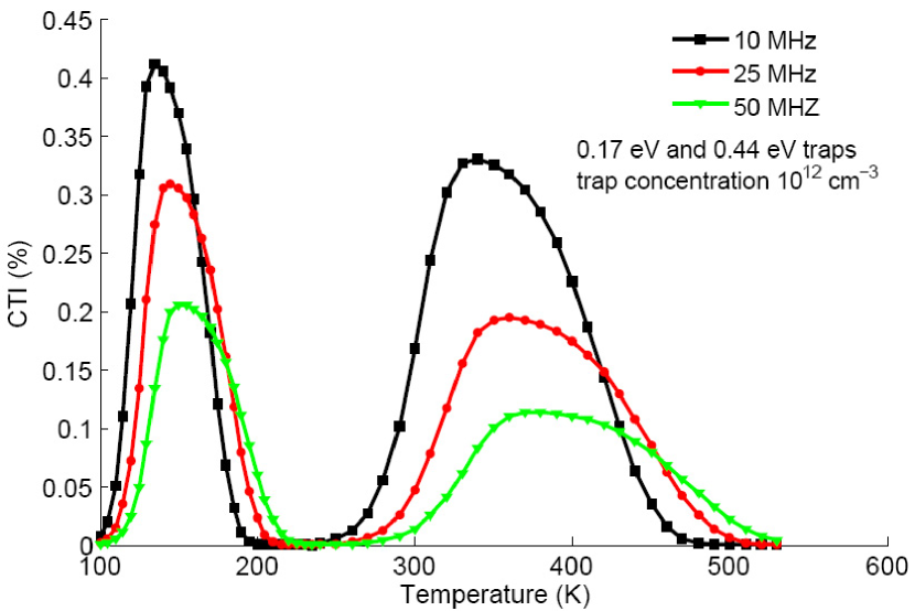
Charge transfer inefficiency (CTI) is an important aspect in the CCD development for operation in High Energy Physics colliders [1, 2, 3]. The LCFI collaboration has been developing new CCD chips and testing them for about 10 years [1, 2, 3, 4, 5]. Recently the focus of the simulations has been on CCDs with column parallel readout (CPCCD). Full TCAD [6] simulations for a CPCCD were performed for different readout frequencies and operating temperatures [7, 8, 9]. An example of the CTI temperature dependence is shown in Fig. 1 (from [9]). Full TCAD simulations are very CPU intensive. This has already been noted for the CCD simulations with a sequential readout [10, 12, 11]. The CTI depends on many parameters, such as readout frequency and operating temperature. Some parameters are related to the trap characteristics like trap energy level, capture cross-section and trap concentration (density). Other factors are also relevant, such as the occupancy of the pixels (hits). It is well known that analytic charge transfer models can be used to study the CTI dependence on readout frequency and operating temperature [13, 14, 15]. For a comparison with full TCAD CTI simulation results, as shown in Fig. 1, we have developed Analytic Models for the CPCCD [7, 8, 9]. The further development of these Analytic Models leads also to better understanding of the relevant parameters in order to reduce the CTI in future CPCCD prototypes. This paper addresses the inclusion of signal shape and clock voltage amplitude which leads to an improved Analytic Model for a CPCCD. The CTI obtained from the improved Analytic Model is compared with results from full TCAD simulations.

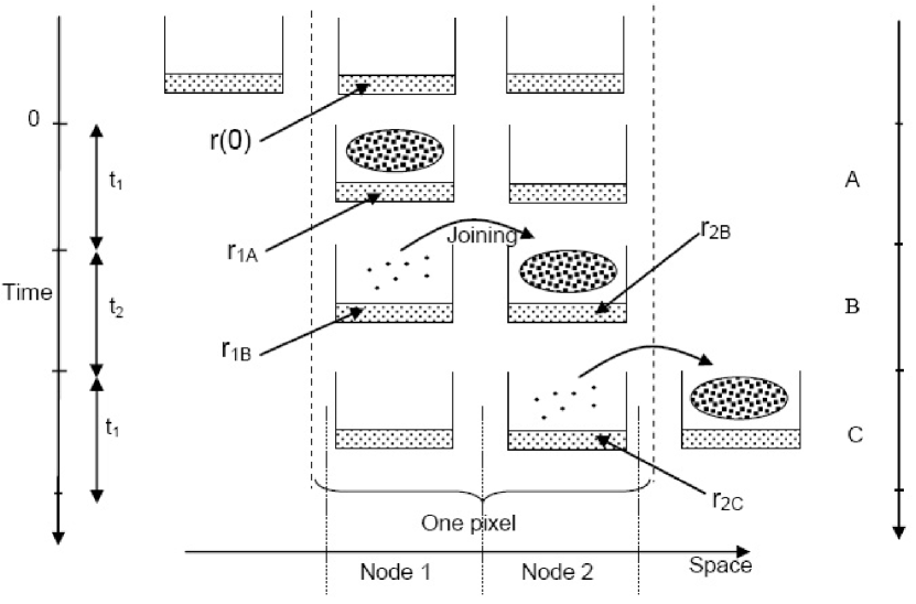
II Analytic Model for CTI determination
The Analytic Models [7, 8, 9] describe the different steps in the charge transfer process and the amount of the trapped charge with respect to the charge cloud in transfer. Figure 2 shows the consecutive charge transfer for a two-phase CPCCD in one pixel (2 nodes). Following the treatment by Kim [16], based on earlier work by Shockley, Read and Hall [17] a defect at an energy below the bottom of the conduction band is considered. Our model considers one single energy level and includes the emission time , and capture time , in the differential equation
| (1) |
where is the fraction of filled traps. Initially the fraction of filled traps is . At stage A the signal charge packet arrives and interacts with traps under node 1 during time . This interaction leads to the capture and emission process. By resolving the differential equation (1), the fraction of filled traps under node 1 during time (when the signal packet is present) is given by
| (2) |
where .
At stage B charge moves to the next node and interacts with traps during time under this node. During this time electrons emitted from node 1 join the signal charge packet in the second node. Thus, the fraction of filled traps under node 1 during time in the presence of the signal packet is given by
| (3) |
At the same stage B, is defined as the fraction of filled traps under node 2 during time , thus,
| (4) |
When the signal charge moves to the first node of the next pixel, stage C, electrons emitted during time can join the signal present at this node and the fraction of filled traps under node 2 during time is given by
| (5) |
The CTI is defined by the ratio of the charge loss under each node to the signal charge density , thus,
| (6) |
where is the trap concentration, and which is determined by considering the fact that initially all traps are filled and electrons are emitted during the waiting time between two signal charge packets. For the case , the combination of the previous equations leads to
| (7) | |||||
III Analytic Model CTI results
The CTI dependence on readout frequency and operating temperature has been explored using an Analytic Model based on Eq. (7). Figure 3 shows the CTI results from the Analytic Model at different frequencies for temperatures between 100 K and 550 K. The CTI increases as the readout frequency decreases. For higher readout frequencies there is less time to trap the passing signal, thus the CTI is reduced. At high temperatures the emission time is so short that the trapped charges can rejoin the passing signal.
IV Comparison between full TCAD simulation and Analytic Model regarding signal shape effect
The signal charge profile varies in the signal cloud as illustrated in the upper part of Fig. 4. The signal packet does not have well defined boundaries and the charge concentration decreases gradually from the centre of the signal packet. Therefore, the signal packet will interact with a varying fraction of the traps within the pixel and this affects the CTI determination. The implementation of a more realistic signal shape into the Analytic Model is expected to improve the agreement with the full TCAD simulation.
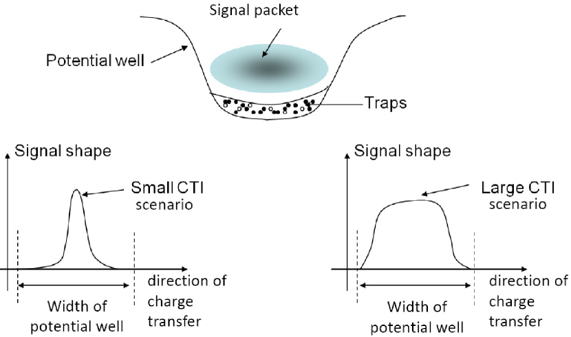
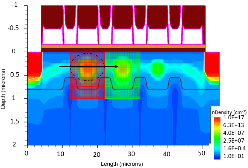
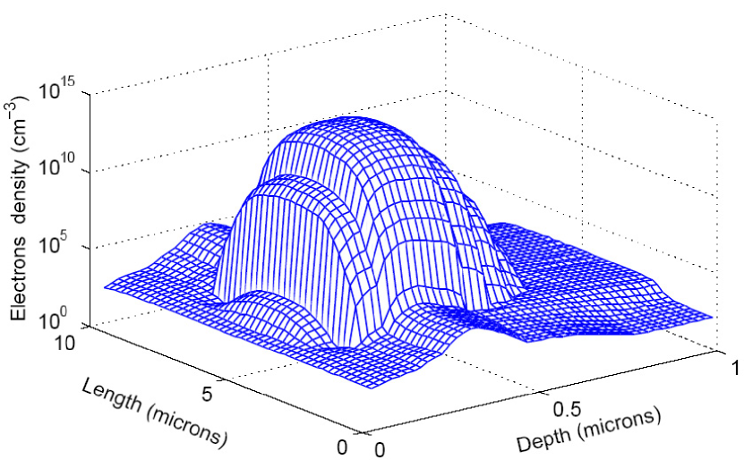
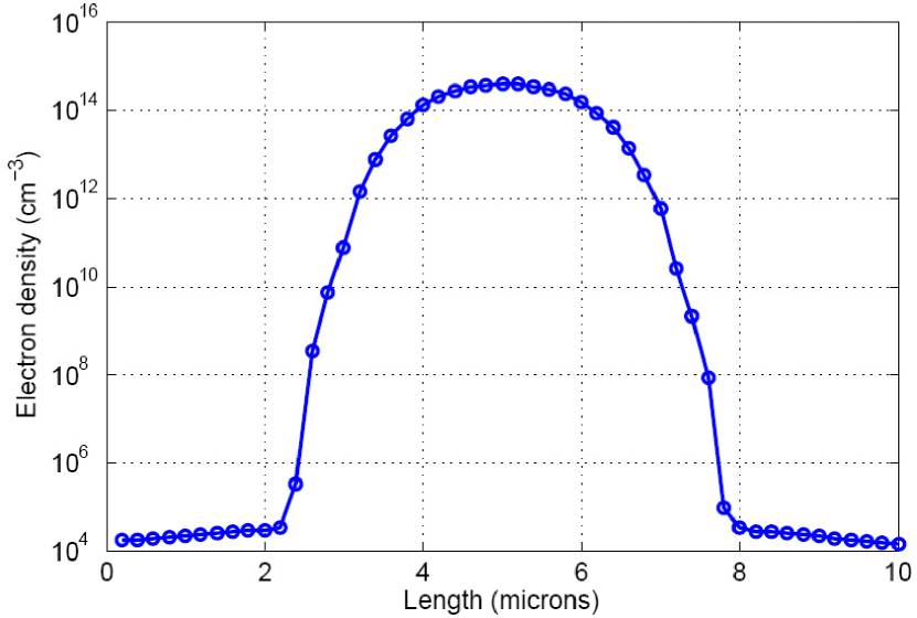
Figure 5 shows the profile of the signal charge under the node from a full TCAD simulation. Two-dimensional and one-dimensional signal charge density profiles are extracted as shown in Figs. 6 and 7, respectively.
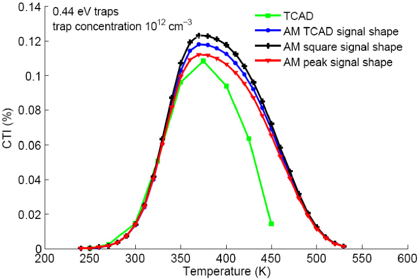
Figures 8 and 9 show the CTI dependence on the signal charge profile for the 0.17 eV and 0.44 eV traps at 50 MHz. These figures also show the CTI values for different signal shapes in comparison with the full TCAD simulation. The CTI is reduced as the width of the potential well becomes smaller. This behaviour is expected, as illustrated in the lower part of Fig. 4. The CTI values calculated with the Analytic Model including the signal charge profile agree better with the full TCAD simulation results. The relatively shallow traps (0.17 eV) are more affected by the signal charge shape than the deeper ones (0.44 eV). The inclusion of the approximate signal shape in the Analytic Model reduces the CTI value in the peak region by about to compared to assuming a square-shape signal.

V Comparison between full TCAD simulation and Analytic Model regarding clock voltage effect
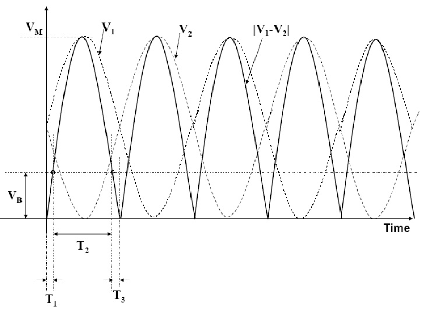
In this study the effect of different clock voltage amplitudes on CTI values are investigated. A sine-form voltage is applied to consecutive nodes as shown in Fig. 10. The following variables are defined:
-
:
voltage applied to a first node of a pixel,
-
:
voltage applied to a second node of a pixel,
-
:
potential barrier created between two successive gates by the doping profile,
-
:
time interval where ,
-
:
time interval where .
The signal is not transferred until the absolute difference between the two clock voltages and reaches the potential barrier created between two consecutive nodes. This affects the CTI determination and it is now included in the Analytic Model. The time intervals and are defined by the intersection point between the curve and the barrier potential (horizontal dashed line): , thus,
| (8) |
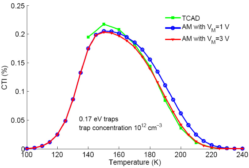
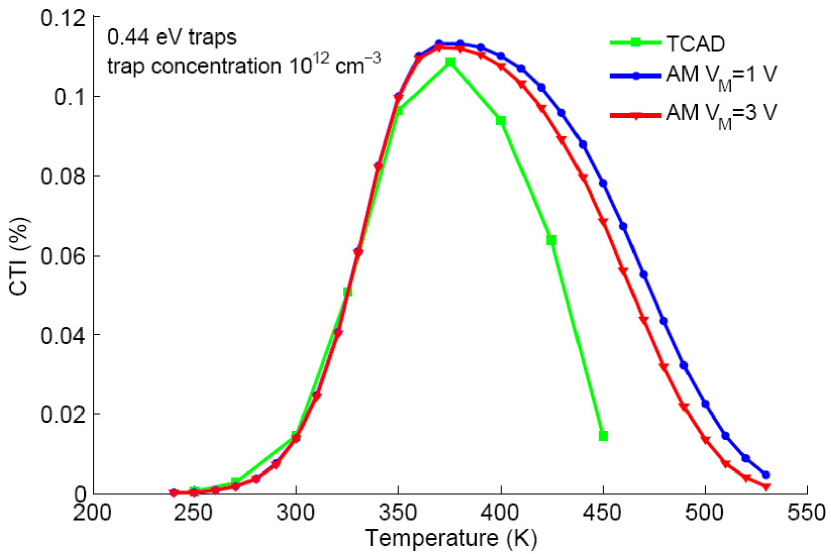
where is the amplitude of the clock voltage. The CTI determined with the Analytic Model including the clock voltage effect is shown in Figs. 11 and 12 for 0.17 eV and 0.44 eV traps, respectively. These results are compared to full TCAD simulations. Two different clock voltage amplitudes are used to illustrate the effect of the clock voltage. It is noted that the CTI decrease occurs only for temperatures above the CTI peak position.
In addition, the effect of the clock voltage amplitude on the CTI is studied for a large variation of amplitudes. The CTI decreases as the amplitude increases until it saturates and no further decrease can be observed. This result is shown in Fig. 13 for two examples, 0.17 eV traps at a temperature of 200 K and 0.44 eV traps at a temperature of 460 K.

VI Conclusions and Outlook
Our previous Analytic Models for a CPCCD have been extended to include the effect of non-uniform signal shape and the effect of realistic clock voltage amplitudes for CTI calculations. The signal shape affects the CTI mostly in the peak region. A smaller width of the potential well decreases the CTI. The inclusion of the clock voltage effects leads to smaller CTI values only above the CTI peak position. In summary, the Analytic Model has been extended to give a more realistic description of the CTI for a CPCCD and the results agree better with full TCAD simulations. Overall, the Analytic Model predicts well the CTI peak position in comparison with a full TCAD simulation. It can produce CTI values almost instantly while the full TCAD simulation is very CPU intensive. Generally, agreement between the Analytic Model and full TCAD simulation results is better for the 0.17 eV traps than for the 0.44 eV traps. The Analytic Model is suited to contribute to future CPCCD developments.
Acknowledgements
This work is supported by the Science and Technology Facilities Council (STFC) and Lancaster University. SA, KB and LD wish to thank the Algerian Government for financial support and Lancaster University for their hospitality. AS would like to thank the Faculty of Science and Technology at Lancaster University for financial support, and the organisers of the IEEE‘08 and IPRD’08 conferences for their hospitality.
References
- [1] C.J.S. Damerell, “Radiation damage in CCDs used as particle detectors”, ICFA Instrum. Bull. 14 (1997) 1.
- [2] K. Stefanov, PhD thesis, Saga University (Japan), “Radiation damage effects in CCD sensors for tracking applications in high energy physics”, 2001, and references therein; K. Stefanov et al., IEEE Trans. Nucl. Sci. 47 (2000) 1280.
- [3] LCFI Collaboration http://hepwww.rl.ac.uk/lcfi/.
- [4] S.D. Worm, “Recent CCD developments for the vertex detector of the ILC – including ISIS (In-situ Storage Image Sensors)”, in 10th Topical seminar on Innovative Particle and Radiation Detectors (IPRD06), Siena, Italy, October 1-5, 2006.
- [5] T.J. Greenshaw, “Column parallel CCDs and in-situ storage image sensors for the vertex detector of the international linear collider”, Nuclear Science Symposium, San Diego, USA, October 29-November 4, 2006.
- [6] DESSIS (Device Simulation for Smart Integrated Systems) from ISE. Version 7.5.
- [7] A. Sopczak et al., “Radiation Hardness Studies in a CCD with High-Speed Column Parallel Readout”, 10th ICATPP Conference on Astroparticle, Particle, Space Physics, Detectors and Medical Physics Applications, Como, Italy, October 8-12, 2007. Proc. World Scientific (2008) p. 599.
- [8] A. Sopczak et al., “Radiation Hardness Studies in a CCD with High-Speed Column Parallel Readout”, Proc. 2007 IEEE Nuclear Science Symposium, Honolulu, USA. Proc. Nuclear Science Conference Record N48-2 (2007) 2278.
- [9] A. Sopczak et al., “Radiation Hardness Studies in a CCD with High-speed Column Parallel Readout”, JINST 3 (2008) 5007.
- [10] A. Sopczak et al., “Simulation of the Temperature Dependence of the Charge Transfer Inefficiency in a High-Speed CCD”, IEEE Trans. Nucl. Sci. 54 (2007) 1429.
- [11] A. Sopczak et al., “Radiation Hardness of CCD vertex Detectors”, IEEE 2005 Nuclear Science Symposium, San Juan, USA. Proc. IEEE Nuclear Science Symposium Conference Record N37-7 (2005) 1494.
- [12] A. Sopczak et al., “Radiation Hardness CCD vertex Detectors for the ILC”, IEEE 2006 Nuclear Science Symposium, San Diego, USA. Proc. IEEE Nuclear Science Symposium Conference Record N14-215 (2006) 576.
- [13] A.M. Mohsen and M.F. Tompsett, “The effects of bulk traps on the performance of bulk channel charge-coupled devices”, IEEE Trans. Elec. Dev. ED-21, 11 (1974) 701.
- [14] I.H. Hopkins, G. Hopkinson and B. Johlander, “Proton-induced charge transfer degradation in CCD’s for near-room temperature applications”, IEEE Trans. Nucl. Sci. 41 (1994) 1984.
- [15] T. Hardy, R. Murowinski and M.J. Deen, “Charge transfer efficiency in proton damaged CCD’s”, IEEE Trans. Nucl. Sci. 45 (1998) 154.
- [16] Ch.-K. Kim, M.J. Howes and D.V. Morgan, “Charge-Coupled Devices and Systems”, Eds. New York: Wiley (1979) 57.
- [17] W. Shockley and W.T. Read, “Statistics of the recombinations of holes and electrons”, Phys. Rev. 87 (1952) 835; R.N. Hall, “Electron-hole recombination in germanium”, Phys. Rev. 87 (1952) 387.