Fast tuning of superconducting microwave cavities
Abstract
Photons are fundamental excitations of the electromagnetic field and can be captured in cavities. For a given cavity with a certain size, the fundamental mode has a fixed frequency f which gives the photons a specific ”color”. The cavity also has a typical lifetime , which results in a finite linewidth f. If the size of the cavity is changed fast compared to , and so that the frequency change f f, then it is possible to change the ”color” of the captured photons. Here we demonstrate superconducting microwave cavities, with tunable effective lengths. The tuning is obtained by varying a Josephson inductance at one end of the cavity. We show data on four different samples and demonstrate tuning by several hundred linewidths in a time . Working in the few photon limit, we show that photons stored in the cavity at one frequency will leak out from the cavity with the new frequency after the detuning. The characteristics of the measured devices make them suitable for different applications such as dynamic coupling of qubits and parametric amplification.
pacs:
85.25.Cp, 42.50.Pq, 03.67.LxI Introduction
Superconducting transmission line resonators are useful in a number of applications ranging from X-ray photon detectors Day et al. (2003) to parametric amplifiers Tholen et al. (2007); Castellanos and Lehnert (2007); Yamamoto et al. (2008) and quantum computation applications Wallraff et al. (2004); Majer et al. (2007); Sillanpaa et al. (2007). Very recently, there has been a lot of interest in tunable superconducting resonators Osborn et al. (2007); Tholen et al. (2007); Castellanos and Lehnert (2007); Sandberg et al. (2008); Placios-Laloy et al. (2007); Yamamoto et al. (2008). In these experiments the inductive properties of the superconductor or a Josephson junction is implemented as a tunable element and is tuned by a bias current or a magnetic field. These devices have both large tuning ranges and high quality factors, we have recently shown Sandberg et al. (2008) that the speed at which these devices can be tuned is substantially faster than the lifetime of the cavity.
The interaction between a qubit and superconducting coplanar waveguide (CPW) resonator can, due to the small mode volume, be very strong when they are resonant with each otherBlais et al. (2004). However, the interaction can be modulated, becoming weak when the qubit and the cavity are off-resonance.
In 2004 Wallraff et al. Wallraff et al. (2004) demonstrated that a superconducting quantum bit, in the form of a Single Cooper pair Box (SCB), could be strongly coupled to a transmission line resonator with a high quality factor. This demonstration opened up a new field of physic known as circuit Quantum Electrodynamics (cQED), it also gave new possibilities of coupling superconducting quantum bits.
The theoretical aspects of using a tunable transmission line resonator for coupling of quantum bits was investigated by Wallquist et al. Wallquist (2006); Wallquist et al. (2006). It was concluded that such a device, with proper characteristics, can be used for dynamic coupling of quantum bits and a protocol for a controlled phase gate was also presented. In this paper fabrication and characterization of a fast tunable superconducting transmission line resonator for the purpose of qubit coupling is described. We show data for four different samples.
II The tunable cavity
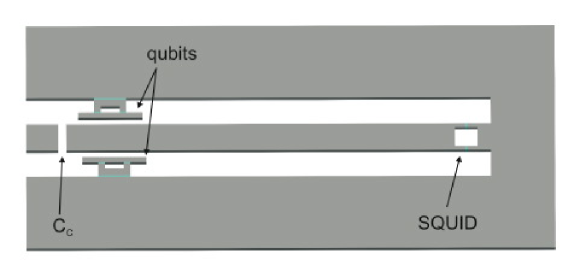
The possibility to achieve strong coupling between qubits and a cavity makes circuit quantum electrodynamics a strong candidate for building a quantum information processor. In the experiment by Majer et al. Majer et al. (2007) where qubit coupling through a cavity was demonstrated and the experiment by Sillanpää et al. Sillanpaa et al. (2007) where state transfer through a cavity was demonstrated the resonance frequency of the cavity was kept fixed while the eigenfrequencies of the qubits could be tuned. The need for fast individual control of each qubit, which can become quite complex with many qubits, could be overcome by using a tunable cavity (see figure 1). There are several different approaches possible for making the resonance frequency of the cavity tunable. Either a characteristic parameter of the transmission line could be varied i.e. the inductance or capacitance per unit length by changing some property of the dielectric or the conductor, or by changing the boundary conditions of the cavity. Here we will focus on tunability obtained by changing the boundary condition of the cavity.
Instead of using a full wavelength resonator as in experiment by Wallraff et al.Wallraff et al. (2004) a quarter wavelength resonator can be used. A quarter wavelength resonator, unlike the full wavelength resonator, is grounded in one end, at the other end the transmission line is open. Due to these boundary conditions resonance occurs for signals with a wavelength such that where is the length of the transmission line and is a non-negative integer.
To make the quarter wavelength resonator tunable the short circuit at one end can be replaced by a tunable impedance. Since the circuit should behave quantum mechanically for the purpose of circuit-QED the tunable impedance must not introduce any large dissipation to the system. One possible tunable impedance fulfilling this criteria is the tunable inductance of a SQUID. The resonator, showed in figure 1, can now be tuned by applying an external magnetic flux to the SQUID loop.
Under the conditions of low temperature and small dissipation electrical circuits can behave quantum mechanically. The quantum mechanical Hamiltonian for such circuits can be obtained starting from the classical Lagrangian. A Legendre transform of the Lagrangian and the imposing of commutation relations gives the Hamiltonian Devoret (1995). The Lagrangian is usually obtained from the kinetic and potential energy of a system expressed in some generalized coordinates and their time derivatives. For an electrical circuit like this we use the capacitive and inductive energy of the components.
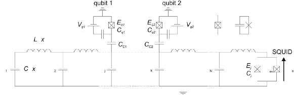
We start from the circuit schematic (ignoring the qubits), see figure 2, and using the procedure for quantization of electrical circuits, following Wallquist (2006); Wallquist et al. (2006). Using the generalized flux, to describe dynamics of the cavity, we get the Lagrangian and the equations of motion. Solving these equations we see that the field inside the cavity must be of the form
| (1) |
where and are the capacitance and inductance per unit length of the transmission line, and where is the wave number of the field that has to be determined. Furthermore, we know have the boundary condition that , where is the average flux over the SQUID. Combining the bulk solution with the boundary condition and assuming small currents gives the dispersion relation
| (2) |
where is the sum capacitance of the SQUID junctions and is the magnetic flux in the SQUID loop. The SQUID is assumed to have identical junctions each with critical current and capacitance . We can then get the wave number by numerically solving the dispersion equation.
A better understanding can be obtained by neglecting the last term in eq. 2 by assuming that is small, which is usually the case. The dispersion relation can then be rewritten as
| (3) |
expanding around (corresponding to a infinite Josephson energy) and using gives the resonance frequency as
| (4) |
where is the quarter wavelength resonance frequency for a sample where the SQUID is replaced by a short, and
| (5) |
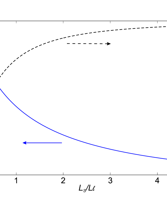
is the inductance of the SQUID. In figure 3 the resonance frequency and its derivative as a function of SQUID inductance is plotted. By applying a magnetic field to the SQUID loop the inductance and hence the frequency of the cavity can be tuned. The qubits can now be addressed individually by the cavity if they have different eigenfrequencies. With this system Wallquist et al. Wallquist et al. (2006) showed that fast dynamic coupling between qubits could be achieved.
III Sample Design
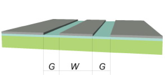
We start be describing the transmission line which consists of a Co-Planar-Waveguide (CPW) with a center strip of width separated by a gap of width from a ground plane on each side, see figure 4. The structure is fabricated on top of some dielectric material with a relative dielectric constant . The characteristic impedance of the transmission line depends on the center strip width, the gap width and the dielectric constant of the dielectric. To obtain a conformal mapping technique can be used Collin (1992). Following the procedure of Gevorgian et al. Gevorgian et al. (1995) we can calculate , the capacitance per unit length and the effective dielectric constant .
To be compatible with the SCB technology Bladh (2005) the aluminum is chosen for the resonator material and it is fabricated on a Si substrate with a wet grown insulating layer of SiO2 with an effective dielectric constant . Choosing the center strip width to be 13 m and a gap width of m, we obtain an impedance = 50 , corresponding to a capacitance per unit length of 164 pF/m.
To be in the range of typical SCB eigenfrequencies the cavity frequency is designed to be GHz. The length of a quarter wavelength resonator is obtained as , where is the speed of light in vacuum.
To probe the cavity it has to be coupled to the outside world, which is done via a coupling capacitance . The coupling capacitance will also lead to leakage of energy out of the resonator and hence to a lower Q value. The (external) Q value for a resonator consisting of an inductance in parallel with a capacitance that is coupled to a load resistance through the capacitance is obtained as
| (6) |
where is the resonance frequency. The same expression is obtained for a quarter wavelength resonator if the capacitance is replaced by . To obtain an external Q-value of for a 5 GHz resonator coupled to a 50 environment we would need a coupling capacitance of . We have used an interdigitated capacitance with only one finger on each side. The approximate length, width and spacing of the fingers were obtained by using the microwave simulation program Microwave Office.
The internal is can be limited by a number of different mechanisms. Here we list four different possible sources of dissipation that can contribute to the internal Q-value. i) At high frequencies some of the electric field will penetrate into the superconductor. At finite temperatures, below the critical temperature , there are still some unpaired electrons above the superconducting energy gap (quasi-particles). The quasi particles causes dissipation when they interact with the electric field. ii) When the cavity oscillates a high frequency current is passed through the SQUID inductance, which will also generate a voltage over the SQUID. This voltage can drive a current though the sub-gap resistance of the SQUID which causes dissipation. iii) There are also losses in the dielectric of the CPW which can lead to dissipation. This is typically described as a complex dielectric constant and a loss tangent. iv) Flux noise in the SQUID loop will cause fluctuations in the resonance frequency and would also result in a larger line width. The sensitivity to flux noise is determined by the derivative . We will return to what limits the internal Q-value.
Next we describe the tunable element which is included in the cavity, namely the Superconducting Quantum Interference device (SQUID). When connecting a Josephson junction or a SQUID to the resonator one has to consider that the junction itself acts as a resonator with a resonance frequency , called the plasma frequency. In order not to excite the SQUID, the resonance frequency of the cavity, must be much less than the SQUID plasma frequency, . This gives the requirement . The capacitance of Al/AlOx/Al Josephson junctions is approximately 45 fF/m2 Delsing et al. (1990). Assuming a 1m2 area this requires A. One also has to make sure that the temperature is low enough so that . This gives the restriction mK on the temperature for a 5 GHz resonator.
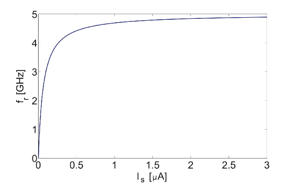
How much can be suppressed by the magnetic field depends on the symmetry of the junctions. The amount that can be suppressed depends on how identical the Josephson junctions can be fabricated. If we assume that they can be fabricated with an within 2% then the minimum is going to be . For the parameters obtained in the last section we see that we have most tunability for low , see figure 5, and for A there is almost no change in resonance frequency. Choosing the critical current in the range of 5 A assuming identical junctions within 2% would then give a tuning range of GHz.
Another consideration is that in the expression for is the total magnetic field in the SQUID loop given by where is the external magnetic field, is the inductance of the SQUID loop and is the screening current in the loop Schmidt (1997). Including the loop inductance and the screening current will also limit the amount that can be suppressed by the magnetic field. Having a small critical current and a small loop inductance reduces this effect.
In order to probe the cavity a signal of a certain power, , has to be applied. The probe signal will cause a current through the SQUID that has to be much less than in order to be in the linear regime. We can derive the expression for the current, at position along the cavity, as a function of power
| (7) |
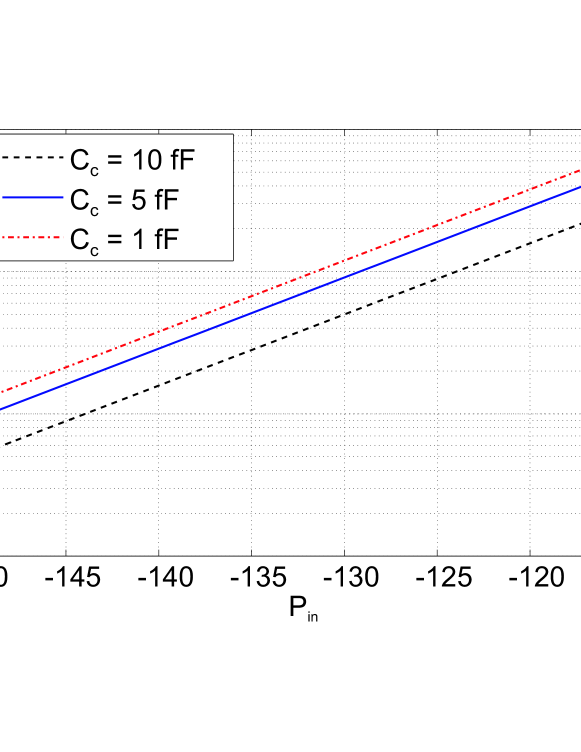
where are the scattering matrix for the coupling capacitance and is the reflection coefficient of the SQUID and is the propagation constant of the transmission line. Assuming an infinite Josephson energy so that the current at the SQUID end as a function of applied power can be obtained, see figure 6. From this we see that in order to be below the minimum of the suppressed current 0.2 A the probe power has to be less than -143 dBm for a coupling capacitance of 5 fF.
To increase the tunability an array of SQUIDs coupled in series could be used for the tuning. The expression for the resonance frequency then modifies to
| (8) |
where is the inductance of each SQUID. The main advantage of this would be that a higher probe power could be used since of each SQUID can be a factor of higher at the same detuning Placios-Laloy et al. (2007). Another approach to obtain large tunability is to make the whole center strip into an array of SQUIDs Castellanos and Lehnert (2007), the tuning is then archived by tuning the phase velocity of the transmission line. Such a setup however, is not well suitable for qubit coupling since the magnetic field has to be applied to the whole resonator structure and hence also to the qubits during the detuning.
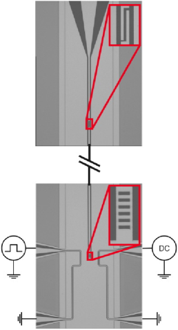
In order to tune the SQUIDs fast, which is necessary for application of quantum gates, a small local field can be used. This is done by current biasing a second transmission line in the vicinity of the SQUIDs. The current needed to apply to the SQUID loop can be approximated by , where is the loop area and is the distance between the bias line and the center of the SQUID loop. The SQUIDs used have an loop area of 30 m2, by placing the bias lines 50 from the SQUIDs a mA is needed (ignoring the effects of flux concentration due to the superconducting ground planes).
IV Experiments
To form the Josephson junctions the two layers of Al were deposited from different angles. After the first layer is deposited a small amount of O2 is let in to the deposition chamber (1 mBar) for a short time (1 min) to oxidize the first layer of Al. The oxide forms a few nm thick insulating layer of AlOx on top of the film. By depositing a second layer of Al after pumping down to base pressure, 5 mBar, but from a different angle, the Josephson junctions of the SQUID are formed. The critical current of the Josephson junctions are determined by the area of the junctions, oxidation pressure and the oxidation time.
The samples were measured in a 3He/4He dilution refrigerator with a base temperature below 20 mK. In order to characterize the samples, high frequency semirigid coaxial cables with a characteristic impedance of 50 were installed in the cryostat. The coaxial cables are stainless steal UT85-SS from the top of the cryostat down to the still level. From the still level down to the mixing chamber superconducting NbTi UT85 cables are used. Well below its critical temperature the NbTi cables have almost no heat conductivity but a very good electrical conductivity. On each stage the cables are thermally anchored using SMA bulk-head feedthroughs and attenuators to thermalize both the outer and the inner conductors.
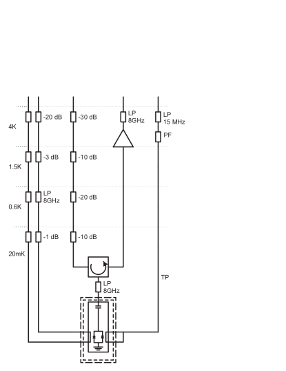
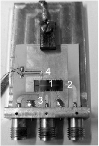
Two different types of samples were studied, one type with on-chip flux bias and the other one without. The samples with on-chip flux bias was mounted in a sample holder on a PCB circuit board, see figure 7. On the circuit board, high frequency lines were fabricated to connect the sample, via wire bonds, to the SMA connectors of the sample holder. A twisted pair cable was also used to supply the sample with a DC flux bias. To protect the sample from external magnetic flux noise a magnetic shield consisting of two inner layers of cryoperm and an outer layer of a superconducting Pb was used. For the other type of sample, without an on-chip flux bias, a single SMA connector directly solder to the PCB was used as a sample holder. On the back side of the PCB a coil was then pattern to apply the magnetic field. To minimize heating the coil was coated with a superconducting Sn-based solder. The coil was connected using twisted pair cable.
In order to use low probe power the samples was probed through a circulator with 18 dB of isolation placed at the mixing chamber of the cryostat, see figure 8. The reflected signal was then amplified by a low-noise cold amplifier mounted to the IVC flange. The amplifier was a Miteq AFS3-04000800-CR-4 with a noise temperature of 5 K measured at 4 K Chincarini et al. (2006) . Using this setup the tunability and tuning speed of the devices was studied. The results of these measurements are presented in the next section.
V Tunability
In this following the results obtained from measurements of the fabricated devices are presented. The tunability of four devices and the tuning speed of one tunable transmission lines resonators have been measured as well as the properties of a non-tunable reference device.
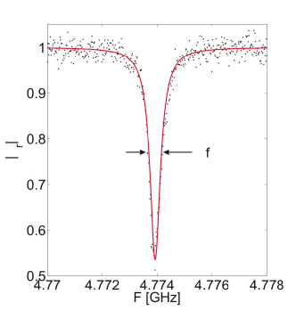
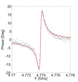
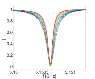
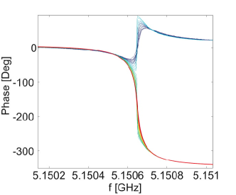
To measure the scattering parameters of the devices a Vector Network Analyzer (VNA) was used. By sweeping the probe signal over a frequency interval a resonance can be detected either in the phase or in the magnitude of the reflection coefficient. A typical measurement is shown in figure 9, where electrical length and losses due to cables and attenuators has been compensated for. From the magnitude response the total value can be obtained as , where is the line width of the resonance and corresponds to the Full Width at Half Maximum (FWHM) of the resonance peak, and is the resonance frequency given by the location of the minimum of the resonance peak. The FWHM and can be obtained by fitting a Lorentzian function to the resonance. The shape of the magnitude and phase response indicated that all the measured resonators were undercoupled, this means that the value is dominated by the internal losses and not by the coupling, i.e. . The total reflection coefficient of the resonator is written as
| (9) |
By fitting to the measurements, assuming only dielectric losses, the parameters of the resonator can be inferred. In order to obtain a god fit, a coupling capacitance of 3 fF for 50 m long fingers and a capacitance of 154 pF/m has to be assumed, slightly less than the design value 164 pF/m. This gives an external value of .
| Sample | ||||||
|---|---|---|---|---|---|---|
| m | GHz | MHz | ||||
| A | 4 | 1 | 25 | 5.062 | 0.0141 | 91 |
| B | 2 | 1 | 50 | 5.025 | 0.0303 | 265 |
| C | 1.2 | 1 | 50 | 5.034 | 0.0537 | 744 |
| D | 2.4 | 6 | 50 | 5.350 | 0.0292 | 580 |
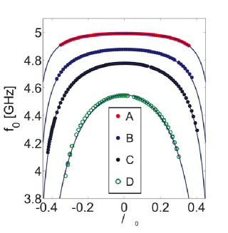
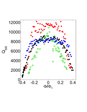
To measure the tunability of the devices a DC magnetic flux bias was applied to the SQUID. In figure 10(a) the resonance frequency as a function of applied magnetic flux for four samples A, B, C and D are shown. The sample parameters are summarized in table 1. The expression for the resonance frequency as a function of flux is given by eq. 8 which is fitted to the measured data with a good accuracy and shown as solid lines in figure 9. In figure 10(b) we have plotted the extracted Q-value as a function of flux. As can be seen the Q-values are typically of the order of at zero flux and it decreases for increasing flux.
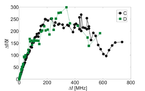
As a figure of merit the tunability can be measured in the number of line widths that the device can be detuned. Since the line width increases with the detuning this has to be compensated for. In figure 11 the number of line widths detuned as a function of detuning is shown for sample C and D. The highest value obtained is around 250 for both samples. The tunability observed for the samples is less than what could be expected if the tunability was only limited by the asymmetry of the SQUID junctions. The limiting factor of the tunability is the strong decrease in value as the applied flux approaches .
VI Reference device
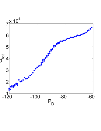
To better understand the source of dissipation inside the resonator a reference device without any SQUID was fabricated. The reference device was measured in the same setup as the other samples. When measuring the response at low drive powers this device was also found to be undercoupled. As the measurement power was increased a transition from undercoupled to overcoupled response was observed, see figure 12. In the undercoupled case the phase goes down a little bit and then back up again while for the overcoupled case the phase goes from 0∘ to -360∘ on resonance. By fitting the reflection coefficient, eq. 9, setting for a short circuit, a coupling capacitance of about 2 fF was obtained for 25 m fingers. This gives a . In figure 13(a) it is seen that the Q value increases with the applied power. The resonator goes from to as the power is increased from -120 dBm to -60 dBm. Due to limitations in the VNA used, more power was not possible to apply without first warming up the cryostat to remove cold attenuators, this was however not done. An increase in as a function of increased drive power was also measured by Martinis et al. Martinis et al. (2005) for a lumped element resonator. They attributed this effect to the existence of two-level systems in the dielectric of their capacitor. As the power is increased the two level systems start to be saturated. As more and more two-level systems get saturated less energy can be absorbed from the resonator and the increases. The amount of two-level systems present in the dielectric depends on the material used and the quality of it. In order to improve the value at low drive power a different dielectric material should be considered.
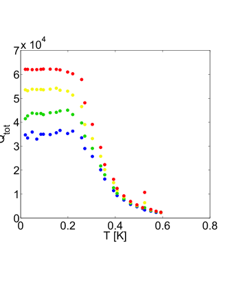
The temperature dependence of the value was also investigated. For low temperatures, T 0.2 K the Q value is independent of temperature, see figure 13(b). As the temperature is increased further the Q value starts to decrease in a way that is consistent with an increase in resistive losses due to thermally excited quasi-particles. Even though the loss mechanisms in our cavities are not fully understood we can say the following. For the cavities presented in this paper our Q-values are limited by intrinsic losses. The thermally excited quasi particles do not seem to limit our Q-value below 200 mK. For zero flux it seems as if the Q-value seems to be due to dielectric losses, but at increased flux there is a different mechanism. The flux noise needed to explain the decrease in Q at large flux would have to bee quite large. Considering our magnetic shielding we do not think it is likely that flux noise is the problem. Instead we believe that the reduction of Q for higher flux is due to the sub-gap resistance in the SQUID junctions. Assuming a sub-gap resistance of approximately would explain the reduction in Q. We would like to point out that the SQUID junctions have relatively high critical current densities which would also lead to a relatively low sub-gap resistance.
VII Fast tuning
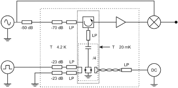
To do fast quantum gates one has to be able to tune the device fast. A measurement scheme where the reflection coefficient is probed as the resonator is detuned is limited by the ring up time of the resonator . For a 5 GHz resonator with a the ring up time is 300 ns. In order to measure tuning speeds faster than this a new measurement setup was implemented. In the new set up, see figure 14, the drive signal is split up. One part of the signal goes down into the cryostat through the circulator and down to the sample. The signal from the resonator goes up through the circulator, through the cold amplifier and in to a mixer at room temperature. The signal from the resonator is there mixed with the other part of the drive signal. The output from the mixer is then filtered through a low pass filter and recorded on a fast oscilloscope. The measurements were performed using a drive power as low as -145 dBm giving approximately 1 photon on average in the cavity. This low photon number was possible using several million averages.
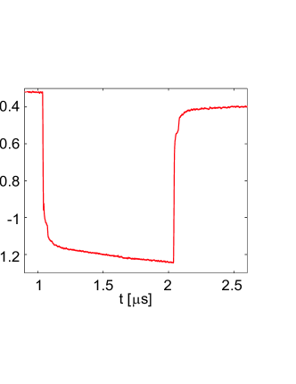
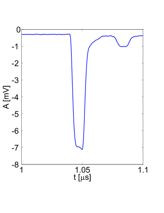
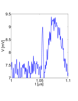
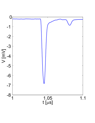
The resonator is tuned, using the DC flux line, in to resonance with the drive signal . On resonance the resonator builds up energy until a steady state is reached. A fast rectangular flux pulse is then applied to the resonators fast flux line that shifts the resonance frequency to a new frequency . The energy stored in the resonator has to adjust its frequency to in order to match the new resonance condition. If no more energy is put into the resonator by the drive signal. The energy that is stored inside the resonator before the detuning starts to leak out through the coupling capacitance. The leakage causes a signal from the resonator, . The signal that leaks out is amplified by the cold amplifier and then put in to the mixer at room temperature. In the mixer the signal from the resonator is multiplied with the other part of the drive signal giving the output signal
| (10) |
The high frequency component of the signal is filtered out using a low pass filter , and the remaining signal can be measured using a fast oscilloscope. The time dependence of the amplitude is governed by the decay of the energy stored in the resonator
| (11) |
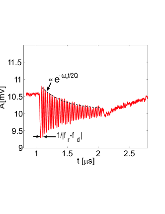
where the factor of 2 comes from the fact that amplitude and not power is measured. From these measurements, the detuning and the value can be obtained, see figure 15.
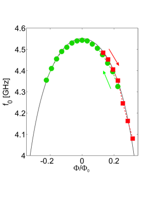
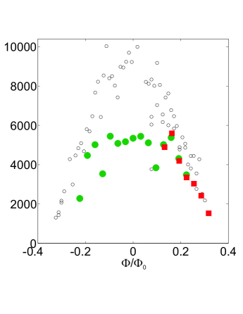
By varying the flux pulses amplitude the resonance frequency as a function of flux can be mapped out, see figure 16. Positive and negative pulses can be applied which means that the frequency can be shifted both to higher and lower values. In order to increase the frequency, work has to be done on the cavity by the applied field while in the case of a decrease in frequency the cavity does work on the field used to tune the resonator. The value as a function of flux pulse is showed in 16 together with the data obtained from measurements of the line width. Due to poor signal to noise ratio the measurement had to be performed several times and averaged, as mention previously.
The value obtained from the decay time measurements differ substantially from the values obtained from the line width around zero flux bias. To understand this discrepancy a histogram of the pulse amplitude from the pulse generator was measured. Using this histogram a probability distribution for the amplitude height can be calculated. Since the amplitude of the flux pulse determine the frequency a distribution in pulse amplitude can be converted into a distribution in frequency. The average measured signal is obtained as
| (12) |
where is the number of bins used in the histograms is the probability of obtaining the frequency . Using the measured histogram the signal can be calculated. If a function is fitted to a is obtained even if a was used in the calculations 12. This calculations suggests that the imperfections of the pulse generator used to create the flux pulses is the cause of the degradation seen in the measured value.
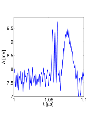
By shortening the duration of the flux pulse, a lower limit on the tuning speed can be obtained. In order to observe oscillations for a flux pulse of length the detuning must be sufficiently large so that , therefore a large amplitude has to be used for the short pulses. figure 17(a) shows the obtained trace for a 10 ns long pulse flux (showed in figure 17(b)), three peaks are observed with a frequency of 330 MHz. There are also some slower oscillations observed after the peaks, these structures are due to reflections of the pulse in the cables. If the pulse is decreased further down to 5 ns one peak can still be observed 18(a). On this sort time scale the pulse starts to be limited by the rise time of the pulse generator 18(b), which is about 2.5 ns. From these measurements it can be concluded that the resonator can be tuned several hundred MHz on a time scale of a few ns.
VIII Conclusions
In conclusion, we have designed and measured several tunable superconducting CPW resonators. We have demonstrated a tunability of more than 700 MHz for a 4.9 GHz device. As a figure of merit, we see that we can detune the devices more than 250 corrected linewidths. We have also demonstrated that our device can be tuned substantially faster than its decay time, allowing us to change the frequency of the energy stored in the cavity. Having done this in the few photon limit, we therefore assert that we can tune the frequency of individual microwave photons stored in the cavity. This can be done by several hundred MHz on the timescale of nanoseconds.
IX Acknowledgments
The samples were made at the MC2 clean room at Chalmers. This work was supported by the Swedish SSF and VR, and by the Wallenberg foundation.
References
- Day et al. (2003) P. K. Day, H. G. LeDuc, B. A. Mazin, A. Vayonakis, and J. Zmuidzinas, Nature 425, 817 (2003).
- Tholen et al. (2007) E. A. Tholen, A. Ergul, E. M. Doherty, F. M. Weber, F. Gregis, and D. B. Haviland, Applied Physics Letters 90, 253509 (2007).
- Castellanos and Lehnert (2007) M. A. Castellanos and K. W. Lehnert, Applied Physics Letters 91, 083509 (2007).
- Yamamoto et al. (2008) T. Yamamoto, K. Inomata, M. Watanabe, K. Matsuba, T. Miyazaki, W. D. Oliver, Y. Nakamura, and J. S. Tsai, Applied Physics Letters 93, 042510 (2008).
- Wallraff et al. (2004) A. Wallraff, D. I. Schuster, A. Blais, L. Frunzlo, R. S. Huang, J. Majer, S. Kumar, S. M. Girvin, and R. J. Schoelkopf, Nature 431, 162 (2004).
- Majer et al. (2007) J. Majer, J. M. Chow, J. M. Gambetta, J. Koch, B. R. Johnson, J. A. Schreier, L. Frunzio, D. I. Schuster, A. A. Houck, A. Wallraff, et al., Nature 449, 443 (2007).
- Sillanpaa et al. (2007) M. A. Sillanpaa, J. I. Park, and R. W. Simmonds, Nature 449, 438 (2007).
- Osborn et al. (2007) K. D. Osborn, J. A. Strong, A. J. Sirois, and R. W. Simmonds, IEEE Transactions on Applied Superconductivity 17, 166 (2007).
- Sandberg et al. (2008) M. Sandberg, C. M. Wilson, F. Persson, T. Bauch, G. Johansson, V. Shumeiko, T. Duty, and P. Delsing, Applied Physics Letters 92 (2008), 203501.
- Placios-Laloy et al. (2007) A. Placios-Laloy, F. Nguyen, F. Mallet, P. Bertet, D. Vion, and D. Esteve, arXiv:0712.0221v1 (2007).
- Blais et al. (2004) A. Blais, H. Ren-Shou, A. Wallraff, S. M. Girvin, and R. J. Schoelkopf, Physical Review A (Atomic, Molecular, and Optical Physics) 69, 62320 (2004).
- Wallquist (2006) M. Wallquist, PhD thesis, Chalmers University of Technology (2006).
- Wallquist et al. (2006) M. Wallquist, V. S. Shumeiko, and G. Wendin, Physical Review B (Condensed Matter and Materials Physics) 74, 224506 (2006).
- Devoret (1995) M. H. Devoret, Quantum fluctuations in electrical circuits, Les Houches, Session LXIII (Elsevire Science, 1995).
- Collin (1992) Collin, Foundations for microwave engineering (McGraw-Hill, 1992), international edition ed.
- Gevorgian et al. (1995) S. Gevorgian, L. J. P. Linner, and E. L. Kollberg, IEEE Transactions on Microwave Theory and Techniques 43, 772 (1995).
- Bladh (2005) K. Bladh, PhD thesis, Chalmers University of Technology (2005).
- Delsing et al. (1990) P. Delsing, T. Claeson, K. K. Likharev, and L. S. Kuzmin, Physical Review B (Condensed Matter) 42, 7439 (1990).
- Schmidt (1997) V. V. Schmidt, The Physics of Superconductors (Springer- Verlag, 1997).
- Chincarini et al. (2006) A. Chincarini, G. Gemme, M. Iannuzzi, R. Parodi, and R. Vaccarone, Classical and Quantum Gravity 23, 293 (2006).
- Martinis et al. (2005) J. M. Martinis, K. B. Cooper, R. McDermott, M. Steffen, M. Ansmann, K. D. Osborn, K. Cicak, O. Seongshik, D. P. Pappas, R. W. Simmonds, et al., Physical Review Letters 95, 210503 (2005).