Anisotropic magnetoresistance in ferromagnetic atomic-sized metal contacts
Abstract
Recent experiments in ferromagnetic atomic-sized contacts have shown that the anisotropic magnetoresistance (AMR) is greatly enhanced and has an asymmetric angular dependence as compared with that of bulk samples. The origin of these effects is still under debate. In this work we present a theoretical analysis of the AMR in atomic contacts of the ferromagnetic materials. Our results strongly suggest that the anomalous AMR stems from the reduced symmetry of the atomic contact geometries. We also present calculations supporting the idea that the pronounced voltage- and temperature dependence in some experiments can be attributed to impurities near the constrictions.
pacs:
73.63.Rt, 75.75.+aWhen a metallic wire is shrunk to the atomic scale, its transport properties are significantly altered Agrait2003 . One interesting and novel example is the anisotropic magnetoresistance (AMR) that arises when the magnetization throughout a ferromagnetic device is rotated uniformly a certain angle with respect to the current direction. In polycrystalline bulk samples such rotation induces a relative change in the conductance that varies as with an amplitude on the order of McGuire1975 . Recently Bolotin et al. Bolotin2006 found that the AMR of permalloy atomic-sized contacts can be considerably enhanced as compared with bulk samples and that it exhibits an angular dependence clearly deviating from the law. Additionally, they found a significant voltage dependence on the scale of millivolts, which led them to interpret the effect as a consequence of conductance fluctuations due to quantum interference Adam2006 . Independently, Viret and coworkers Viret2006 reported similar results in Ni contacts, but also the occurrence of conductance jumps upon rotation of the magnetization. Similar stepwise variations of the conductance have been found in Co nanocontacts Sokolov2007 .
The jumps have been interpreted as a manifestation of the so-called ballistic AMR (BAMR) Velev2005 . According to this theoretical concept the rotation of the magnetization in a ballistic contact could result in an additional band crossing the Fermi energy, leading to an abrupt change in the conductance on the order of . This has been theoretically shown to occur in ideal infinite chains of Ni and Fe Velev2005 . However, realistic ferromagnetic contacts made of transition metals are not expected to be ballistic Untiedt2004 and so the interpretation of the conductance jumps in terms of BAMR is at least questionable. Indeed, Shi and Ralph Shi2007a have suggested that these jumps might originate from two-level fluctuations due to changes in atomic configurations Shi2007b . Thus, there remain important open questions about AMR in atomic contacts, concerning the origin of the enhanced amplitude, the anomalous angular dependence, the occurrence of conductance jumps, and the voltage dependence.
In this Letter we address these questions using a combination of a tight-binding (TB) model, molecular dynamics (MD) simulations, and a simple toy model. Our calculations suggest that the enhancement of the AMR amplitude and the deviations from the law in atomic contacts stem from spin-orbit coupling (SOC) together with a reduced symmetry of the contact geometry. We do not find signs of BAMR in realistic contact geometries. Finally, we find that the conductance of pure atomic contacts has no voltage dependence on the the scale of millivolts, but the addition of impurities can lead to a significant voltage dependence of the AMR signal.
Our description of the AMR in ferromagnetic atomic contacts of the 3 metals (Ni, Co, and Fe) is based on the following non-orthogonal TB Hamiltonian that includes the SOC:
| (1) |
Here run over the atomic sites, denote the different atomic orbitals, and the spin. The spin-polarized parameters and the spin-independent overlaps are taken from the parametrization of Refs. Mehl1996 ; Bacalis2001 , which is known to accurately reproduce the band structure and total energy of bulk ferromagnetic materials and has been successfully applied to the description of ferromagnetic atomic contacts Haefner2008 ; Pauly2006 . The atomic basis is formed by 9 orbitals (), which give rise to the main bands around the Fermi energy in Fe, Co, and Ni. The matrix elements of the intra-atomic SOC are given by , where and are the orbital and spin angular momentum operators. These matrix elements depend on the spin quantization axis (with polar angle and azimuthal angle ), which we rotate uniformly to simulate the AMR experiments with saturated magnetization. We use the SOC constant meV, which is the experimental value for Ni. We stress that, while this type of model is not expected to be as accurate as ab initio counterparts, it captures the essential physics. It also has the advantage that it allows us to analyze phenomena like BAMR in realistic contact geometries, which is currently outside the scope of ab initio methods.
In order to describe the electronic transport we use the nonequilibrium Green’s function formalism Additional_material . Briefly, the atomic contacts are divided into three parts, a central region containing the constriction and the left/right (/) leads, which we model as infinite surfaces. The retarded Green’s functions of the central part read
| (2) |
where are the lead self-energies (). Here, , with , the hopping elements and overlaps between the region and the lead , and is a surface Green’s function. In general and depend on the bias voltage . The -dependent transmission matrix is , where . The current then adopts the standard Landauer-Büttiker-like form
| (3) |
where are the Fermi functions and is the transmission function. The low-temperature linear conductance can be written as , where are the transmission coefficients, i.e. the eigenvalues of at Fermi energy .
In the calculations presented here we have neglected the SOC in the leads. We have checked that this only introduces a small change in the contact resistance that does not alter the conclusions but reduces the computation time enormously. On the other hand, we determine self-consistently the on-site energies of the atoms in the constriction by imposing the local charge neutrality that metallic elements should exhibit.
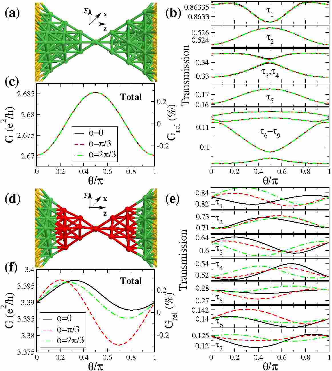
We now apply this method to calculate the conductance of Ni atomic contacts. First we consider an ideal geometry with the atoms kept fixed on fcc lattice positions and forming pyramid-like tips in the direction that end in a common central atom [Fig. 1(a)]. In Figs. 1(b,c) the conductance and its channel decomposition as function of for several values of are shown. Surprisingly, the conductance of this one-atom contact exhibits the bulk-like AMR with a dependence (minimum at ), an amplitude of and practically no dependence on . In fact, the individual channels show a more complicated dependence on , and the amplitude of variation for one channel can be bigger than that of the total conductance, but in the latter these features cancel and the dependence is recovered.
It seems obvious that the cancellation is related to the high symmetry of the ideal geometry. To test this idea we have distorted the contact by shifting randomly the atomic positions by up to of the nearest-neighbor distance [Fig. 1(d)]. As seen in Fig. 1(e), the individual channels now show roughly the same amplitude of variation with as in the ideal contact, but due to the disorder they exhibit a more complex dependence, and a strong dependence on . As a consequence, the contributions of the channels no longer cancel out and the AMR can have a different amplitude, with the conductance extrema shifted in and with a strong dependence on [Fig. 1(f)]. This example illustrates that the origin of the anomalous angular dependence and amplitude of the AMR in atomic contacts can be simply the reduced symmetry of these junctions together with the fact that the conductance is mainly determined by a few atoms in the narrowest part of the constrictions. We want to point out that we have found similar results for Co and Fe atomic contacts, which confirms this conclusion Additional_material .
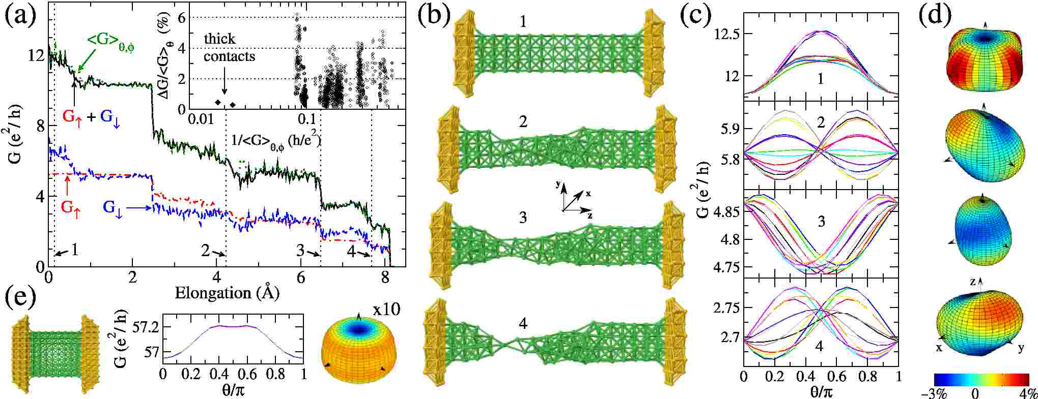
Since the geometry plays such a prominent role in the AMR, it is important to determine the geometries that can be realized in an actual experiment. For this purpose, we have carried out classical MD simulations of the formation of Ni atomic contacts, following Ref. Pauly2006 . An example of the contact evolution is shown in Fig. 2. Here, we start with an ideal Ni bar containing 112 atoms on lattice sites in fcc direction. The bar is attached to rigid surfaces that are separated in a stepwise manner, simulating the elongation process of a break junction. In Fig. 2(a) we show the evolution of the spin-projected and total conductance during elongation in the absence of SOC. Adding SOC introduces only a small change in the averaged total conductance. As usual, the sudden atomic rearrangements are reflected as steps in the conductance Agrait2003 . The vertical lines refer to the geometries of Fig. 2(b) obtained during the elongation. For them we have computed the dependence of the conductance on and , and the results are shown in Fig. 2(c). For contact 1, which is just an elastic deformation of the ideal contact, the conductance has two types of behavior depending on : one is -like, while the other is clearly more complex. In order to visualize the overall angular dependence, we show the relative AMR on a “Bloch sphere” [Fig. 2(d)]. The contact 1 and hence its AMR have an approximate four-fold symmetry. When deformations emerge in the contact, the angular dependence becomes irregular and strongly dependent on . For example, for contact 2 there is a strong variation of AMR with , and depending on its value, the AMR amplitude can be almost one order of magnitude larger than in the bulk limit or cancel almost entirely. As the contact evolution proceeds, the AMR has an amplitude of around . In almost all cases, the conductance is not only shifted in , but it also has a more complicated behavior than just . Approaching the tunnel regime (), we do not observe a further increase of the AMR amplitude, contrary to experiments Bolotin2006 . One reason may be that the isolated tip atoms in tunneling regime exhibit a finite orbital moment Desjonqueres2007 (not considered here), which may lead to a local deviation of the spin-quantization axis from the field direction and an additional increase in resistance. Finally, in the limit of thick contacts, we recover bulk behavior with an amplitude of , as shown in Fig. 2(e). The statistical analysis of all contact geometries shows an increase of AMR to on average in the last steps before breaking, see inset of Fig 2(a). This confirms that the lack of symmetry in atomic contacts gives rise to the enhancement of the AMR signal.
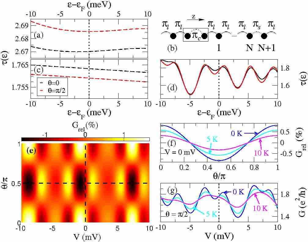
We have not found indications of tip resonances, which are present in ideal one-dimensional geometries Burton2007 ; Jacob2008 and which were suggested as the origin of the experimental findings Burton2007 . For example, the transmission for the contact of Fig. 1(a) has almost no structure around on the scale of millielectronvolts, as shown in Fig. 3(a). We thus believe that the voltage and temperature dependences reported in Refs. Bolotin2006 ; Shi2007b are indeed associated with impurities close to the constriction, as reported earlier for non-magnetic junctions Ludoph1999 ; Untiedt2000 . Following Ref. Untiedt2000 , one may estimate that the reported Bolotin2006 voltage period of a few millivolts can stem from impurities located hundreds of nanometers away from the contact. Such length scales cannot be modeled realistically, but we have developed a toy model to support the idea. As represented schematically in Fig. 3(b), we model the contact with two semi-infinite linear chains connected at the tips, and describe the system with a nearest-neighbor TB Hamiltonian. For simplicity we only include the and orbitals (the doublet), with a spin-splitting of eV. In the absence of SOC there are four independent equivalent chains with onsite energies , hopping integrals eV in the leads, and eV between the tip atoms. The SOC that couples the chains is restricted to the two tip atoms, with a coupling constant eV. For further details, see Ref. Additional_material . As we show in Fig. 3(c), there is no structure in and the AMR is small due the high symmetry of the geometry. In this example eV, which makes the sign of the AMR opposite to that in Fig. 3(a). We note that the results of Fig. 1(b) are qualitatively reproduced Additional_material .
Things change drastically when an impurity is introduced in one of the chains. We model it by using slightly reduced hoppings eV between two atoms sites away from the constriction in the right lead. Figure 3(d) shows the resulting transmission functions for . In addition to the expected oscillations in energy, there appears a modulation depending on that stems from the interference with the impurity. When a finite voltage is applied over the tip atoms, the nonlinear conductance exhibits oscillations as a function of both voltage and the angle . The relative variations shown in Fig. 3(e) bear a striking resemblance to the experimental results of Ref. Bolotin2006 . Finally, we show in Figs. 3(f,g) the temperature dependence of both the linear and non-linear conductance. The effect of temperature is to smooth the K characteristics, again compatible with the experimental observations Shi2007b .
In summary we have shown that the anomalous magnitude and angular dependence of the AMR in ferromagnetic atomic-sized contacts can be explained naturally in terms of the reduced symmetry of the atomic junction geometries. We predict a strong anisotropy of the conduction channels, but have not found any signature of BAMR. We have presented a simple model which illustrates that the pronounced voltage and temperature dependence found in some experiments may originate from the presence of impurities close to the constriction.
We thank M. Dreher, G. Schön, A. Levy Yeyati, N. Agraït, M. Viret, and E. Scheer for helpful discussions. We acknowledge support from the Helmholtz Gemeinschaft (Contract No. VH-NG-029), and the DFG within the CFN. MH also acknowledges support by the KHYS.
References
- (1) N. Agraït, A. L. Yeyati, and J. M. van Ruitenbeek, Phys. Rep. 377, 81 (2003).
- (2) T. McGuire and R. Potter, IEEE Trans. Magn. 11, 1018 (1975).
- (3) K. I. Bolotin, F. Kuemmeth, and D. C. Ralph, Phys. Rev. Lett. 97, 127202 (2006).
- (4) S. Adam, M. Kindermann, S. Rahav, and P. W. Brouwer, Phys. Rev. B 73, 212408 (2006).
- (5) M. Viret et al., Eur. Phys. J. B 51, 1 (2006).
- (6) A. Sokolov, E. Y. Tsymbal, J. Redepenning, and B. Doudin, Nature Nanotech. 2, 171 (2007).
- (7) J. Velev, R. F. Sabirianov, S. S. Jaswal, and E. Y. Tsymbal, Phys. Rev. Lett. 94, 127203 (2005).
- (8) C. Untiedt, D. M. T. Dekker, D. Djukic, and J. M. van Ruitenbeek, Phys. Rev. B 69, 081401 (2004) and references therein.
- (9) S.-F. Shi and D. C. Ralph, Nature Nanotech. 2, 522 (2007).
- (10) S.-F. Shi, K. I. Bolotin, F. Kuemmeth, and D. C. Ralph, Phys. Rev. B 76, 184438 (2007).
- (11) M. J. Mehl and D. A. Papaconstantopoulos, Phys. Rev. B 54, 4519 (1996).
- (12) N. Bacalis, D. Papaconstantopoulos, M. Mehl, and M. Lach-hab, Physica B 296, 125 (2001).
- (13) M. Häfner et al., Phys. Rev. B 77, 104409 (2008).
- (14) F. Pauly et al., Phys. Rev. B 74, 235106 (2006).
- (15) For more details, see supplementary online material.
- (16) M.-C. Desjonquères, C. Barreteau, G. Autès, and D. Spanjaard, Phys. Rev. B 76, 024412 (2007).
- (17) J. D. Burton et al., Phys. Rev. B 76, 144430 (2007).
- (18) D. Jacob, J. Fernández-Rossier, and J. J. Palacios, Phys. Rev. B 77, 165412 (2008).
- (19) B. Ludoph, M. H. Devoret, D. Esteve, C. Urbina, and J. M. van Ruitenbeek, Phys. Rev. Lett. 82, 1530 (1999).
- (20) C. Untiedt, G. Rubio Bollinger, S. Vieira, and N. Agraït, Phys. Rev. B 62, 9962 (2000).