Modulation of Electrical Conduction Through Individual Molecules on Silicon by the Electrostatic Fields of Nearby Polar Molecules: Theory and Experiment
Abstract
We report on the synthesis, scanning tunneling microscopy (STM) and theoretical modeling of the electrostatic and transport properties of one-dimensional organic heterostructures consisting of contiguous lines of CF3– and OCH3–substituted styrene molecules on silicon. The electrostatic fields emanating from these polar molecules are found, under appropriate conditions, to strongly influence electrical conduction through nearby molecules and the underlying substrate. For suitable alignment of the OCH3 groups of the OCH3–styrene molecules in the molecular chain, their combined electric fields are shown by ab initio density functional calculations to give rise to potential profiles along the OCH3–styrene chain that result in strongly enhanced conduction through OCH3–styrene molecules near the heterojunction for moderately low negative substrate bias, as is observed experimentally. Under similar bias conditions, dipoles associated with the CF3 groups are found in both experiment and in theory to depress transport in the underlying silicon. Under positive substrate bias, simulations suggest that the differing structural and electrostatic properties of the CF3-styrene molecules may lead to a more sharply localized conduction enhancement near the heterojunction at low temperatures. Thus choice of substituents, their attachment site on the host styrene molecules on silicon and the orientations of the molecular dipole and higher multipole moments provide a means of differentially tuning transport on the molecular scale.
pacs:
31.70.-f, 68.37.Ef, 68.43.-h, 73.63.-bI Introduction
During the last decade a great deal of research has focussed on electrical conduction through individual moleculesRatner06 ; Tao06 ; GK . Many molecules are electrically polarized due to chemical charge transfer between unlike atoms. This results in electric fields that should influence electrical conduction through such molecules and through molecules in their vicinity. However, there have been few direct experimental investigations of such effects in the context of molecular-scale nanoelectronics. Recently experimental studies of the effects of charged chemical species attached to a molecule on electrical conduction through the same molecule have been reported Venk2ring ; Venkataraman . The presence of a charged dangling bond on a silicon surface has been observed to affect electrical conduction through nearby moleculesNature and, conversely, transport through adjacent silicon atoms has been found to be perturbed by dipole fields due to molecules located elsewhere in the Si 77 cellHarikumar . However, no experimental work directly probing the effects of electric fields emanating from polar molecules on electrical conduction through other individual molecules has been reported to date. This topic is explored experimentally and theoretically in the present article.brief The influence of these electric fields on electrical conduction through the underlying semiconductor substrate to which the molecules are bound is also examined.brief
The specific systems that we study here are one-dimensional (1D) organic heterostructures consisting of chains of substituted styrene molecules grown on hydrogen-terminated Si substrates by the self-directed growth mechanism described by Lopinski and coworkersLopinski originally for styrene on H:Si(100) 21 but subsequently applied to a wide range of molecules. The substituents in the present work are CF3 and OCH3 groups, one of which replaces a single hydrogen atom bound to the aromatic carbon ring of each styrene molecule. In each case the substituent is in the “para” position. Each heterostructure consists of a line of surface bound OCH3–styrene molecules joined end-to-end (at the heterojunction) to a line of CF3–styrene molecules. The OCH3 group donates electrons to the aromatic ring of the styrene and is therefore positively charged while the CF3 group withdraws electrons and is negatively charged. However, electric polarization also occurs within the CF3 and OCH3 groups themselves and we find the resulting molecular multipole fields to also play an important role in electrical conduction in these systems.
In the experimental work presented here electrical conduction between the silicon substrate and a tungsten scanning tunneling microscope (STM) tip via the molecular heterostructures was measured at room temperature in ultra-high vacuum under a variety of bias conditions. Strongly enhanced conduction was observed through a group of several OCH3–styrene molecules near the heterojunction at low and moderate negative substrate bias. Under positive substrate bias similar pronounced enhancement of the molecular conduction near CF3–styrene/OCH3–styrene heterojunctions was absent. In related heterostructures, CF3–styrene lines in a side-by-side configuration were found to locally depress transport originating from filled states in the underlying silicon. As will be explained below these qualitative differences can be understood as arising from the different structural, electronic and electrostatic properties of OCH3–styrene and CF3–styrene molecules on silicon.
The OCH3–styrene/CF3–styrene heterowires were modeled theoretically by determining their ground state electrostatic potential profiles (at zero applied bias) by means of ab initio density functional theory-based computations, and then employing semi-empirical tight binding models together with the ab initio electrostatic profiles, solution of the Lippmann-Schwinger equation and Landauer theory to calculate the electric current between the tungsten STM tip and the silicon substrate under bias via the molecular heterostructure. We note that while the use of density functional theory for performing transport calculations in molecular wires lacks a fundamental justification and is increasingly being questioned in the literature,Delaney ; Sai ; Toher05 ; Darancet ; Evers ; Ke07 ; Pemmaraju ; Prodan ; offsets ; Koentoppreview ; Thygesen78 ; Toher78 ; Thygesen8 ; GK the use of density functional theory to calculate ground state electrostatic potentials is justified (at least in principle) by a lemma proved originally by Hohenberg and Kohn. HK The usefulness of such density functional theory-based electrostatic potential calculations for the present system is supported also by the fact that the present theory is able to explain the experimentally observed phenomena outlined in the preceding paragraph.
The theoretical work that is presented here demonstrates that electric fields due to intramolecular charge transfer within OCH3–styrene and CF3–styrene molecules can (for appropriate molecular geometries) result in enhanced electrical conduction through certain molecules in chains of OCH3–styrene and CF3–styrene molecules on silicon, consistent with the experimental STM data: These electric fields shift the energies of the molecular HOMO and LUMO states of like molecules in different parts of the chain by differing amounts with the result that resonant conduction begins at lower bias voltages on some molecules in the chain than on others. The differences in the observed behavior under positive and negative applied bias and between the OCH3–styrene and CF3–styrene molecules are accounted for in terms of this electrostatically modulated resonant transport mechanism.
The present theory predicts that conduction through individual molecules in such systems can be changed by orders of magnitude by varying the conformations of (and hence the arrangement of charges in) molecules in their vicinity. This raises the possibility of molecular switches of a new type that depend for their operation not on conformational changes in the molecular wire carrying the current (as has been discussed previouslyswitch1 ; switch ; switch2 ) but on conformational changes in other nearby molecules that result in changes in the energy level structure of the molecular wire. An advantage of a conformational switch based on this different principle is that the molecular wire that carries the current need not be a moving part in the device. The shorter range of electrostatic fields due to molecular dipoles (and higher multipoles) than those of electric monopoles such as the charged dangling bond studied in Ref. Nature, is also advantageous, making it possible in principle to achieve higher densities of molecular switches controlled by molecular dipoles in potential device applications. The greater chemical stability of a polar molecule than a charged radical is also an important advantage. Furthermore manipulating the orientations of molecular dipoles may be an attractive alternativedipole to inducing switching by charging and discharging atomic or molecular-scale constituents of the ultimate nanoscale electronic devices.
This article is organized as follows: The experimental methodology and results are presented in Section II. The theoretical model is explained and justified in Section III. A discussion of the relevant energy level ordering in these systems is presented in Section III.2. The different structures that the molecules may assume when bound to silicon are described in Section III.3. Our theoretical results for a particular conformation of a OCH3–styrene/CF3–styrene molecular chain on silicon are presented in Section IV for positive and negative substrate bias, together with some comments as to how these theoretical results may relate to the experimental data. In Section V we clarify the relationship between structure, electric potentials and transport in the OCH3–styrene/CF3–styrene heterostructures by considering systematically other examples of possible molecular chain geometries. Theoretical results demonstrating that the current enhancement near the OCH3–styrene/CF3–styrene junction is specifically an electrostatic effect are reported in Section VI. Simulations of heterostructures that include single and triple rows of CF3–styrene molecules and of the influence of these molecules on the electrostatic potentials in the underlying silicon and on electron transport are reported in Section VII. Further discussion of the relationship between the theory and experiment is presented in Section VIII.
II Experiment
STM experiments were performed under vacuum on hydrogen-terminated Si (100) 21 surfaces. Samples were cleaved from arsenic-doped (resistivity 0.005 cm) Si (100) oriented wafers, and mounted into molybdenum sample holders. Samples were loadlocked into a vacuum system (background pressure 110-10 Torr) and degassed at for 8 hours. The samples were flash annealed to to remove the surface oxide and re-order the crystal surfaces. During annealing, heating was temporarily suspended if the system pressure exceeded 410-10 Torr. Clean crystalline surfaces were routinely produced with defect densities below 5%.
After cool down and inspection in the STM, the silicon crystals were transferred to the preparation chamber for hydrogen termination. Molecular hydrogen was leaked into the system (110-6 Torr) and a hot tungsten filament () positioned 10 cm from silicon sample () dissociated the molecular gas into reactive atomic hydrogen. A 13 minute exposure produced samples with a quasi-saturated 2 1 silicon monohydride surface.Boland
One dimensional molecular organic heterowires were grown under vacuum using the self-directed growth mechanism reported by Lopinski and coworkersLopinski for styrene on H:Si(100) 21. For styrene (consisting of an aromatic carbon ring bound to a vinyl group), self-directed growth results from a chain reaction between the vinyl group of the styrene and a surface dangling bond (i.e. silicon radical exposed by a missing hydrogen atom on the surface). In forming a chemical bond with the exposed silicon atom, the terminal carbon atom on the vinyl group breaks one of its double bonds to the adjacent carbon atom, leaving the unsatisfied bonding electron on the adjacent carbon atom to abstract a hydrogen atom from an adjacent Si dimer. The newly formed dangling bond is then free to repeat the process by reacting with another styrene molecule. Multiple reactions lead to well ordered one dimensional chains of styrene bound along a given side of a silicon dimer row. Lopinski
This self-directed growth mode has been observed to occur for various alkene and carbonyl containing molecules including functionalized styrenesDiLabio ; Tong ; Kruse ; Piva making the formation of heterowires a simple matter of sequentially dosing the H:silicon surface with the desired chemical precursors.caveat The fortuitous alignment of the aromatic rings in these structures make them ideally suited for probing transport effects resulting from overlapping and * states along the molecular chain axis. The introduction of a chemical discontinuity at the heterojunction provides a means of isolating and studying effects resulting from specific intermolecular interactions. Electron donating and withdrawing substituent groups are of particular interest as they modify the energy alignment and spatial distribution of and * states in host aromatic molecules. These effects lead to systematic variations in reaction ratesHammett and ionisation potentialsDiLabio99 ; Anagaw in substituted aromatic compounds. Corresponding effects on single molecule transport are under current investigation.Venkataraman
Substituent effects in STM imaging of 4-methylstyrene/styrene heterowires were reported in Reference stymeth, . While the substituted methyl group had a strong (bias dependent) influence on the differential molecular height and corrugation resolved on either side of the heterojunction, the imaging characteristics of the heterowires could be understood qualitatively without considering the effects of intermolecular electrostatic interactions on the electronic structure of the heterowires; features reflecting such interactions were not observed in the experimental data. The present work revisits the earlier heterowire line-growth experiments with more strongly perturbing substituent groups:DiLabio99 ; Anagaw 4-methoxystyrene (OCH3–styrene), and 4-trifluoromethylstyrene (CF3–styrene).
H-termination of the Si(100) samples, growth of the molecular heterowires and their imaging with an Omicron STM1 were all carried out within the same vacuum system. Dissolved atmospheric gases were removed from the substituted styrene precursors using multiple freeze-pump-thaw cycles prior to introduction (via leak valve) into the vacuum system. Before and after line growth, samples were imaged in STM using electrochemically etched tungsten tips, cleaned by electron bombardment, and field emission. Bias dependent STM imaging of the structures was performed in constant-current mode (tunnel current fixed at 40 pA). Surface coordinates belonging to STM images in Figures 1 to 3 were rescaled after acquisition to yield an orthogonal inter-row (0.768 nm) to inter-dimer (0.384 nm) periodicity of 2:1. Feature heights in the constant-current STM images were determined in relation to observed terrace height separation on the Si(100) surface (0.136 nm). Images of CF3–styrene/OCH3–styrene heterowires were acquired on multiple surfaces and studied using several different tips in two separate Omicron STM1 systems.
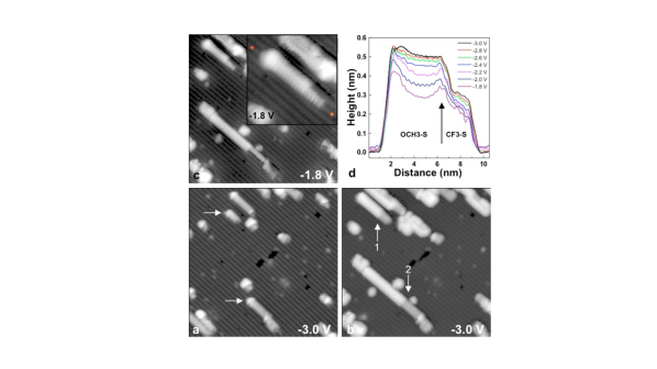
Figure 1 shows the growth and bias dependent STM imaging of two CF3–styrene/OCH3–styrene heterowires on an H:silicon sample. After imaging the unreacted H:silicon surface (not shown), the STM tip was retracted micron from the surface. CF3–styrene was introduced into the chamber at a pressure of 110-6 Torr for seconds. Sample exposure was nominally 10L (1L = 10-6 Torr sec). The H-terminated silicon dimer rows run diagonally between the upper left and lower right hand corners of the image frames. The elongated white (elevated) features running along the dimer rows correspond to regions where molecules have reacted with the surface. The black (depressed) features appearing most notably in the centers of Figs 1 (a) and (b) result from missing atoms (Si vacancies) in the silicon surface.
Fig.1(a) shows a 26nm26nm region of the sample following the 10L exposure of CF3–styrene. Sample bias () was V. White arrows label the reactive dangling bonds at the end of two CF3–styrene line segments. Due to slight tip asymmetry, CF3–styrene bound to either side of their host dimers image with slightly different corrugation. Comparison with images of the unreacted H:silicon surface (not shown) show the upper and lower CF3–styrene line segments are chemically bound to the right-hand and left-hand sides of their respective dimer rows.
Fig.1(b) shows the same region of the crystal (V) following a 10L exposure of OCH3–styrene (1 10-6 Torr exposure for seconds). The terminal dangling bonds belonging to the upper and lower CF3–styrene line segments in (a) have reacted with OCH3–styrene forming two CF3–styrene/OCH3–styrene heterowires (‘1’ and ‘2’). At V, the tip Fermi-level is below the highest band of occupied molecular states for the OCH3–styrene as evidenced by the fact that at this bias voltage the experimental STM height profile of the OCH3–styrene has saturated as can be seen in Fig.1(d): This saturation indicates that the number of OCH3–styrene HOMO states contributing to the STM current is no longer increasing with increasing bias so that the STM tip Fermi level must be below the highest band of OCH3–styrene HOMO levels. However, the tip Fermi-level remains above the occupied molecular states in the CF3–styrene at this bias because the molecular CF3–styrene HOMO is well below the OCH3–styrene HOMO as evidenced by gas phase molecular calculationsDiLabio99 and by the present theoretical work for these molecules on silicon. This is also consistent with the CF3- styrene molecules imaging with reduced height (less bright) in comparison to the OCH3–styrene in Fig.1.
Fig.1(c) shows the same region of the crystal imaged with = -1.8 V. At this bias, the tip Fermi-level is in the vicinity the highest occupied molecular orbitals ( states) in the OCH3–styrene line segment; this conclusion is based on comparisons between these experimental data and the results of our theoretical modeling as is discussed in Section IV.2. While the OCH3–styrene continues to image above (brighter than) the CF3–styrene, heterowires 1 and 2 image with enhanced height (brighter) above the OCH3–styrene molecules situated near the heterointerface. The OCH3–styrene molecules in heterowire 1 (close-up in inset) near the terminal dangling bond also image with increased height.
Fig.1(d) shows a series of 0.4nm wide topographic cross-sections extracted from heterowire 1 along the trench running between its attachment dimer row (labelled with red circles in Fig.1(c) inset) and the vacant H-terminated dimer row to its right. Also included are curves from images (not shown) acquired at intermediate sample biases. The topographic height envelope for the heterostructure extends between 1 nm and 9.5 nm along the abscissa. The height maxima associated with the terminal dangling bond, and the molecular heterojunction are located at 2.3 nm, and 6.4 nm, respectively. Postponing discussion of the interfacial height enhancement for the time being, the bias dependent height response of the OCH3–styrene line segment near the terminal dangling bond is much like that reported in Ref.Nature, for a single homomolecular styrene line segment: At elevated negative substrate bias, ( V) the highest band of occupied states in the OCH3–styrene lies above the tip Fermi-level and the OCH3–styrene images with roughly uniform height. As the bias decreases in magnitude, these occupied states of the OCH3–styrene approach the tip Fermi-level (and eventually begin to drop below it), and the molecules image with reduced height above the surface. Molecules in the vicinity of the negatively charged dangling bond on the degenerately doped n-type surface exhibit a spatially dependent reduction in ionisation potential due to the electrostatic field emanating from the negatively charged dangling bond.Nature ; Raza Thus at low bias, molecules nearest the terminal dangling bond image with increasing height.Nature
In stark departure from the imaging characteristics of homomolecular styrene chains reported in Ref.Nature, , and absent from the images of the CH3–styrene/styrene heterowires studied in Ref.stymeth, is the height enhancement at the heterojunction resolved at low bias. The bias-dependent height response of the OCH3–styrene near the heterojunction is similar to that near the terminal dangling bond just described. At elevated bias, the interfacial OCH3–styrene images with nearly constant height along the bulk of the homowire segment. As decreases, however, the height of the interfacial OCH3–styrene (4-5 molecules closest to the molecular interface) does not decay as rapidly as in the mid-section of the OCH3–styrene line segment. At the lowest filled-state bias studied for this particular heterowire, the interfacial OCH3–styrene molecules image nm higher than OCH3–styrene molecules situated 5-7 dimers away from the heterojunction. The typical noise in the presented images is nm.
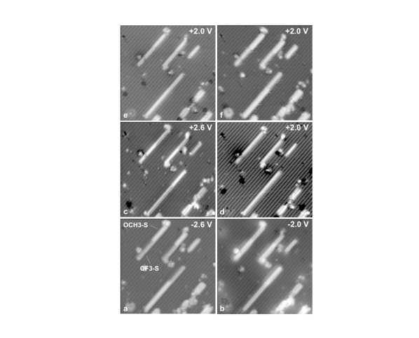
Fig.2 shows filled and empty-state imaging of a cluster of 3 heterowires. These heterowires were identified on a region of the crystal where imaging of the H:silicon surface before line growth was not carried out. The chemical identities of the line segments were confirmed at the end of the imaging sequence by dosing with CF3–styrene, and comparing the imaging characteristics of the newly reacted line segments (not shown) with the nearby heterowires. Characteristics in these images (in combination with those in Fig.1) are representative of the range of tip-dependent imaging contrast encountered over the course of the experiments.
Fig.2(a) shows a filled-state constant current STM image of the 3 heterowire cluster with V. As in Fig.1(b), the OCH3–styrene line segments image taller (brighter) than the CF3–styrene line segments consistent with their relative ionisation potentials. In Fig.2(b) (V), however, the OCH3–styrene away from the interface images lower (darker) than the CF3–styrene. This contrast reversal (tip dependent) is often encountered at low bias in filled-state imaging. In all instances, whether or not this low bias contrast reversal occurs, height enhancement of the interfacial OCH3–styrene remains prominent and corresponds to the height of OCH3–styrene far from the interface at greater magnitude filled-state bias (i.e. the interfacial OCH3–styrene images as though accompanied by a localised increase in effective tip-sample bias magnitude).
Figs 2(c) to (f) show empty-state images for the 3 heterowire cluster. In Fig.2(c) at V, the CF3–styrene images above (brighter than) the OCH3–styrene. As is discussed in Section IV.2 this result is consistent with the increased electron affinity of the CF3–styrene (a result of the highly electronegative F atoms). As the * state for the CF3–styrene is much lower than the corresponding * states belonging to the OCH3–styrene, a greater number of tip states can tunnel into the CF3–styrene (and therefore, the STM tip must travel further away from the surface above the CF3–styrene to maintain a constant tunnel current across the heterostructure). In Fig.2(d), V and the tip Fermi-level is presumed to lie below both the OCH3–styrene (as before) and CF3–styrene * states. The tunnel current is dominated by carrier injection into the silicon conduction band, and the molecules image (non-resonantly) with similar contrast.
Figs 2(e) and (f) display empty-state imaging data acquired at = +2.0 V following spontaneous tip structural changes. In this imaging mode, the OCH3–styrene images above (brighter than) the CF3–styrene. This imaging behaviour when apparent, often extends to greater bias (up to = +3.2 V). In addition to this empty-state contrast reversal, changes to the molecular corrugation within the homomolecular line segments are apparent (particularly in terms of the appearance of the OCH3–styrene between frames (d) and (f)). It is clear in these experiments that the tip density of states plays a considerable role in determining the contrast (in terms of overall height and/or molecular corrugation) observed between the OCH3–styrene and CF3–styrene line segments. Tip-dependent imaging contrast in STM of organic molecules has been documented previously.Cyr ; Hahn
While the empty-state imaging displays considerable contrast variation, of particular significance is the absence of notable interfacial structure. An exception to this was observed in a small portion of low bias empty-state images which revealed height enhancement for a single interfacial molecule. The height enhancement was between 0.01 to 0.02 nm, and smaller than the 0.02 nm to 0.14 nm height enhancement observed for the considerably broader ( molecule wide) filled-state interfacial features resolved in Figs 1(c)-(d), 2(b), and others (not shown). While such a narrow empty-state feature appears in the simulation work presented in Sections IV and V, additional observations will be required before a detailed comparison with theory can be undertaken.
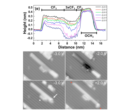
Fig. 3 shows STM imaging results for a CF3–styrene/OCH3–styrene heterostructure with multiple CF3–styrene chains in a side by side configuration. Fig. 3(a) shows a region of the H:silicon surface following a 10 L exposure of CF3–styrene ( V). The arrow points to the reactive dangling bond at the end of the longest CF3–styrene line. The marks a short double chain of CF3–styrene that has grown beside the long CF3–styrene chain. Figures 3(b) to 3(d) show the same region following a 10 L exposure of OCH3–styrene. The end of the long CF3–styrene chain has been extended by approximately 7 molecules of OCH3–styrene. Figures 3(b) (V) and 3(c) (V) image the single and triple CF3–styrene segments with comparable height. In Fig. 3(d), has been reduced to V and the region with the triple CF3–styrene lines images below (darker than) the single file chain of CF3–styrene. Fig. 3(e) shows topographic cross sections along the CF3–styrene/OCH3–styrene heterowire. From V to V, the triple CF3–styrene chain (between 7 and 10 nm along the abscissa) images with decreasing height. Significantly, at V, this region images 0.2 nm below the H:Si surface indicating depleted silicon state density beneath the molecules at the tip Fermi level.
Results presented in Figures 1 and 2 and for other single chain CF3–styrene/OCH3–styrene heterostructures (not shown), show the presence of the chemical heterojunction causes the interfacial OCH3–styrene to image with elevated height under low filled-state bias. The prominence (both in terms of height and lateral extent) of the filled-state interfacial feature compared with the absence of significant interfacial structure resolved in empty-state imaging in these structures, suggests an electronic origin for the effect. As the low bias imaging conditions required to observe the filled-state interfacial feature also result in decreased tip-sample separation, the possibility of tip-molecule interactions at the heterojunction leading to altered molecular conformations which contribute to the observed interfacial structure cannot be ruled out. However, such tip-induced structural changes cannot account for the differing interfacial behaviour observed at low positive and negative substrate bias. The localized depletion in silicon filled-state density observed in Fig. 3 (typical of other side by side CF3–styrene structures studied) in response to the triple CF3–styrene chains also cannot be understood in terms of only conformational differences between otherwise non-interacting molecules. The theoretical modeling developed in the following Sections explores various factors which can account for these observations. It will be seen that conformational details in concert with electrostatics play a significant role in these phenomena.
III Model
III.1 Formalism
In order to carry out calculations of electronic transport through molecules bonded chemically to metal or semiconductor electrodes it is necessary to know the electronic structures of these systems. Ab initio density functional calculations based on the Kohn-Sham local density approximation (LDA) KohnSham and extensions such as generalized gradient approximations (GGA) are commonly used for this purpose. However, the theoretical foundations of this approach and the accuracy of the results that it yields for molecular transport calculations are increasingly being questioned in the literature at the present time:Delaney ; Sai ; Toher05 ; Darancet ; Evers ; Ke07 ; Pemmaraju ; Prodan ; offsets ; Koentoppreview ; Thygesen78 ; Toher78 ; Thygesen8 ; GK While such formalisms are appropriate (at least in principle) for calculating the total energy, the spatial distribution of the electronic charge density and the electrostatic potential throughout inhomogeneous electronic systems in their ground states,KohnSham ; HK the single-electron eigenenergies and wave functions that appear in them are somewhat artificial constructs that in most cases do not have rigorous physical meanings.KohnSham ; GK ; Evers ; Koentoppreview Consequently, they need not be good approximations to the energies and wave functions of the true electronic quasi-particles that determine the electronic transport properties of molecular systems. Under what circumstances such ab initio calculations should produce acceptable results for electron transport despite this fundamental shortcoming, and how to obtain satisfactory results when they do not are important unresolved questions that are the subject of much ongoing research at the present time.Delaney ; Sai ; Toher05 ; Darancet ; Evers ; Ke07 ; Pemmaraju ; Prodan ; offsets ; Koentoppreview ; Thygesen78 ; Toher78 ; Thygesen8 ; GK ; Buker
For molecules adsorbed on silicon the above deficiencies of the LDA, GGA and their relatives manifest themselves most obviously in that these approximations underestimate the band gap of silicon and yield incorrect values for the energy offset between the highest occupied molecular orbital (HOMO) of the molecule (or the relevant frontier orbital of the adsorbate) and the silicon valence band edge. The errors in these energy offsets obtained from the density functional calculations have recently been estimated for a few molecules to range from 0.6 to 1.4eV.offsets Because of these and otherRakshit deficiencies, the predictions of transport calculations based on ab initio density functional calculations of the electronic structure are unreliable for molecules on silicon; they are able to capture some observable phenomenaBevan but are qualitatively incorrect for others.offsets ; stymeth
In the case of linear chains of styreneLopinski and methyl-styrenestymeth molecules grown by self-assembly on a hydrogenated (001) silicon surface, the incorrect offsets between the molecular HOMO levels and the silicon valence band edge given by the density functional calculations result in such calculations yielding qualitatively incorrect STM images for these systems.stymeth In particular, at low bias the ab initio calculations predict minima in the STM height profiles of the molecular chains over the centers of the molecules where maxima are observed experimentally.stymeth These deficiencies of the ab initio calculations have been overcomestymeth by developing a different electronic structure model based on extended Hückel theory, a tight binding scheme from quantum chemistry Hoffman ; Ammeter that provides an approximate description of the electronic structures of many molecules and has also been used successfully to explain the experimental current-voltage characteristics of a variety molecular wires connecting metal electrodesDatta ; Emberly ; EmberlyPRB ; Kushmeric ; Cardamone and to model the band structures of a variety of crystalline solids stymeth ; Cerda ; Kienle
Extended Hückel theory describes molecular systems in terms of a small set of Slater-type atomic orbitals , their overlaps and a Hamiltonian matrix . The diagonal Hamiltonian elements are taken to be the atomic orbital ionization energies and the non-diagonal elements for are expressed in terms of , , and phenomenological parameters chosen for consistency with experimental molecular electronic structure data. As is described in detail in Ref. stymeth, , the standard extended Hückel theoryAmmeter was modified so as to also provide an accurate description of the band structures of the silicon substrate and the tungsten STM tip. The energy offset between the molecular HOMO and the silicon valence band edge (an adjustable parameter in the theorystymeth ) was assigned a physically reasonable value for which our transport calculations reproduced correctly the character of the height profile along the styrene and methylstyrene molecular chains observed experimentally in STM images at low bias, i.e., apparent height maxima over the centers of the molecules. The model proved to be remarkably successful, accounting not only for this low bias property of the STM images, but also for several counter-intuitive features of the experimental data, including the experimentally observed reversal in the contrast between the styrene and methyl-styrene molecular chains with increasing STM tip bias, the observed increase in the apparent height of the molecules at the ends of the molecular chains relative to those far from the ends with increasing bias and the observed disappearance of the corrugation of the STM height profile along the molecular chains with increasing bias.stymeth
The tight binding model based on extended Hückel theory that is described in Ref. stymeth, is adopted in the present work but with an important modification: A limitation of extended Hückel theory is that in it the atomic orbital energy depends on the type of atom on which orbital is located but is not influenced by the presence of other atoms in the vicinity. This is a reasonable first approximation for the styrene and methylstyrene molecules considered in Ref. stymeth, since those molecules do not contain strongly charged groups. However for the OCH3-styrene and CF3–styrene molecules that will be considered here, there is strong charge transfer between carbon atoms and fluorine and oxygen atoms that results in significant electrostatic fields that should modify the atomic orbital energies of surrounding atoms. These electrostatic fields are included in the present model as is explained below. The resulting variation in the electrostatic potential from molecule to like molecule along the molecular chains has direct and striking effects on the experimental STM height profiles presented in Section II, as will be discussed in detail in the Sections that follow.
While, as has been discussed above and in Refs. Delaney, ; Sai, ; Toher05, ; Darancet, ; Evers, ; Ke07, ; Pemmaraju, ; Prodan, ; offsets, ; Koentoppreview, ; Thygesen78, ; Toher78, ; Thygesen8, ; GK, , the use of density functional theory at the level of LDA or GGA for calculating electronic quasiparticle properties has no fundamental justification, this criticism does not apply to calculations of the ground state electronic charge density distribution and the electrostatic potentials that that have been shown by Hohenberg and KohnHK to be functionals of the charge density. Therefore the use of ab initio density functional calculations to estimate the electrostatic contributions to the atomic orbital energies that are due to charge transfer between different atoms (but are neglected in extended Hückel theory), while still involving approximations, is justified at the fundamental level. In the present work these electrostatic corrections to extended Hückel theory were included in our model in the following way:
An ab initio calculation was carried outGaussian of the electrostatic potential at the nucleus of every atom of an atomic cluster that included a molecular chain with a total of 20 OCH3–styrene and CF3–styrene molecules in the geometry that they take on the silicon surface, a few layers of nearby Si atoms, and the H atoms needed to passivate the dangling bonds on the surface of this silicon cluster. A similar ab initio calculation was carried outGaussian of the electrostatic potential at the nucleus of each of these atoms in the absence of all of the other atoms. Thus
| (1) |
is an estimate of the contribution to the electrostatic energy of an electron in an atomic orbital on atom that is due to the presence of all of the other other atoms in the system, calculated self-consistently from first principles. I.e., it is the electrostatic contribution to the atomic orbital energy that is neglected in extended Hückel theory, as discussed above. This contribution was included in the present model by making the substitution (for each atomic orbital of every atom ) in the diagonal elements of the extended Hückel-like model Hamiltonian obtained for this system as described in Ref.stymeth, . Because the orbital basis used is not orthogonal (as in standard extended Hückel theory), the non-diagonal matrix elements of the model Hamiltonian were also adjusted according to for orbitals and on atoms and as required for gauge invariance.shift The effect of the bias voltage applied experimentally between the STM tip and the silicon substrate on the Hamiltonian matrix was included in the present model as in Ref.stymeth, .
Since in the above theoretical approach a highly compute-intensive ab initio calculation of the effects of charge transfer is carried out only once for any molecular chain being studied and a smaller basis set is used in the transport calculations that follow, in addition to correcting some fundamental deficiencies of density functional theory as discussed above, the present approach is able to treat much larger systems than is practical to study by ab initio methods alone. This was crucial for the present work where fairly long molecular chains on Si needed to be studied and the system is not periodic along the molecular chain.
The electric current flowing between the STM tip and silicon substrate via the adsorbed molecules was evaluated as described in detail in Ref. stymeth, by solving the Lippmann-Schwinger equation, determining from the solution the Landauer transmission probability that depends on the electron energy and applied bias voltage and evaluating the Landauer formula
| (2) |
where is the current, and is the electrochemical potential of the source () or drain () electrode.temp
The chains of OCH3–styrene and CF3–styrene molecules and associated silicon clusters that needed to be studied theoretically to make comparison with the experiment included too many atoms for it to be practical to determine their relaxed structures using density functional theory calculations. Therefore a molecular mechanics method was adopted: Chains of 40 molecules, half of the chain OCH3–styrene and the other half CF3–styrene, on a hydrogenated silicon cluster were relaxed using the Universal Force Field modelGaussianUFF starting from a variety of initial configurations, and many different metastable relaxed structures were found. It is reasonable to suppose that many of them as well as intermediate structures between them were being sampled thermally in the experiment which was carried out at room temperature. Thus the limited accuracy of the structures given by the molecular mechanics method was deemed to be adequate for the purpose of the present study. Since the phenomena of interest in the present work were observed experimentally near the junction of the OCH3–styrene and CF3–styrene chains, the relaxed molecular chain was truncated to a subset of 20 molecules surrounding the junction and the calculations of the electrostatic potential and of electrical conduction between the silicon substrate and STM tip via the molecules were carried out for this truncated chain of molecules and underlying H-terminated Si cluster with a dimerized (001) surface without further relaxation. The STM tip in the present work was modelled as in Ref.stymeth, as a 15 tungsten atom cluster with a (001) orientation and a single terminating atom, and coupled to an electron reservoir by many ideal leads.
III.2 Energy Level Ordering
In the present theoretical approach, the energy offsets between the HOMO levels of the OCH3–styrene and CF3–styrene parts of the molecular chain are given by the extended Hückel theory with the parameterization described in Ref. Ammeter, , modified so as to yield an accurate band structure for silicon and to include the ab initio electrostatic corrections as discussed in Section III.1. The same applies to the molecular LUMO levels and to the variation of the atomic orbital energies from molecule to molecule along the molecular chain.
The molecular HOMO and LUMO levels for both types of molecules considered here reside primarily on the benzene rings of the molecules. Thus, because of the electron withdrawing (donating) nature of the CF3 (OCH3) group, the OCH3–styrene HOMO is higher in energy than the CF3–styrene HOMO,DOS and the CF3–styrene LUMO is lower than the OCH3–styrene LUMO. Thus the HOMO of the molecular chain as a whole is located on its OCH3–styrene part (as has already been mentioned in Section II) and the LUMO of the molecular chain as a whole is located on its CF3–styrene part.
However, as in Ref. stymeth, , the energy offset between the molecular HOMO of the molecular chain and the silicon valence band edge is an adjustable parameter of the present theory whose value is not known accurately: As was discussed at the beginning of Section III.1, this offset is not given correctly by calculations based on standard density functional theories; its accurate determination (like the determination of the energy offsets between the molecular levels and substrate Fermi levels for other molecular nanowiresRatner06 ; GK ) is a difficult unsolved problem of molecular electronics. However, based on the discussion of our experimental results that follows it is plausible that the molecular HOMO is located below the silicon valence band edge and the molecular LUMO is located above the silicon conduction band edge:
An important aspect of the experimental data presented in Section II is that even for the smallest values of , the bias voltage voltage between the STM tip and substrate at which imaging of the molecular chains was feasible, was considerably larger than the band gap of silicon, for both positive and negative biasing of the silicon substrate relative to the STM tip. Given that the Fermi level of the STM tip at zero bias is located within the Si band gap, it therefore follows that the STM tip Fermi level was well below the top of the silicon valence band or well above the bottom of the silicon conduction band when the molecules were being imaged for negative and positive biasing of the substrate relative to the STM tip, respectively. A reasonable interpretation of this fact (that is consistent with all of the experimental data and with the results of our theoretical modeling) is that the HOMO of the molecular chain is located in energy below the silicon valence band edge, that the LUMO of the molecular chain is above the silicon conduction band edge, and that the experimental imaging of the molecular chains themselves (in the present study) was being carried out for STM tip Fermi energies near or above the LUMO or near or below the HOMO of the molecular chain, conditions under which enhancement of STM currents due to resonant or near resonant transport via the molecules is to be expected. This will be the view adopted in the remainder of this article.
Thus three regimes will be considered theoretically for both positive and negative substrate bias:
1. Very low bias at which the STM tip Fermi level lies between the Si conduction band minimum (valence band maximum) and the molecular LUMO (HOMO) energy levels.
2. Low bias at which the STM tip Fermi level is slightly above (below) the lowest (highest) molecular LUMO (HOMO) level.
3. Higher bias at which the STM tip Fermi level is near the top (bottom) of the lowest (highest) molecular LUMO (HOMO) band.
As will be seen below, each regime is predicted to have its own characteristic signature in STM imaging that can be compared with our experimental data. These signatures do not depend qualitatively on the precise value assumed for the offset between the silicon valence band edge and molecular HOMO level. Thus comparison between theory and experiment allows us to draw conclusions regarding the specific regimes in which the data was being taken and the physical mechanisms underlying the phenomena that were observed.
III.3 Prototypical Geometries of the Individual Molecules Bound to Si Dimers
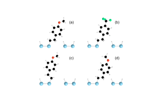
Different conformations have been proposed for styrene molecules on H terminated Si(100)Lopinski ; stymeth ; Cho and it is reasonable to suppose that different atomic geometries are possible for the substituted styrenes on Si that are studied here. One possibility is that the C atom of the molecule that bonds to the C atom that bonds to the Si is located over the “trench” between two Si dimer rows as is shown in Fig.4(a) for OCH3–styrene and in Fig.4(b) for CF3–styrene. This conformation is similar to that assumed for chains of styrene molecules on Si in Refs Lopinski, and stymeth, and will be referred to as “the T-tethered geometry”. In another conformation that has also been proposed for styrene on SiCho the C atom that bonds to the C atom that bonds to the Si is located over the the Si dimer row to which the molecule bonds as in Fig.4(c); this alternate conformation will be referred to as “the D-tethered geometry.” In Fig.4(a) and (c) the C atoms of the OCH3 groups are located further over the “trench” than the O atoms are, i.e., the OCH3 group also has the T orientation. However, the opposite (D) orientation of the OCH 3 group with the C oriented towards the Si dimer to which the molecule bonds as shown in Fig.4(d) is also possible.
The molecular conformations described above are ideal cases: Molecule-molecule interactions in the molecular chains and thermal motion at room temperature are expected to result in many intermediate geometries with the molecular benzene ring and the CO bond of the OCH3 group not being coplanar with each other or with the silicon dimer to which the molecule bonds and the OCH3 and CF3 groups being rotated through different angles about the bonds that link them to their respective molecules. As will be seen below, these deviations from the ideal geometries need to be taken into consideration when modeling the experimental STM images of the molecular heterowires. However it will often be convenient in the discussions that follow to classify molecular structures according to the idealized structures such as those in Fig.4 (T or D tethered molecule, T or D oriented OCH3 group) that they most closely resemble.
IV Theoretical Results for a representative molecular chain geometry
IV.1 Structure
In this Section we present theoretical results for electrical conduction between the STM tip and Si substrate through a particular 20-molecule CF3–styrene/OCH3–styrene chain on the dimerized H-terminated (001) silicon surface. The relaxed geometry of a part of this molecular chain surrounding the CF3–styrene/OCH3–styrene junction is shown at the top of Fig. 5. Atoms are colored as in Fig.4. Each molecule bonds to a Si atom on the same edge of the same Si dimer row (the far edge of the dimer row closest to the viewer) through a single C-Si bond as in Fig.4. For the specific geometry shown in Fig. 5 the tethering of all of the molecules to the Si as well as the orientations of the OCH3 groups are of the T type defined in Section III.3. Some further details of this structure should also be noted since they shall prove to be crucial in making the connection between the theoretical results that will follow and key aspects of our experimental data: Most of the molecules lean somewhat in the direction away from the heterojunction and also have swung outwards somewhat (away from the heterojunction) about the axes of the tethering Si-C bonds, as one might expect for molecules subject to a net weak mutual steric repulsion. Due to the repulsion between the F atoms on different CF3–styrene molecules, the CF3 groups are all rotated through different angles about the bonds between the CF3 groups and the molecules’ benzene rings, and the benzene rings themselves are tilted somewhat differently from molecule to molecule. Because of this the detailed structure of CF3–styrene chain is more complex and less well ordered than that of the OCH3–styrene chain.
IV.2 Theoretical current profiles at positive and negative substrate bias
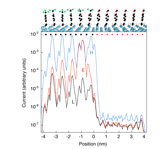
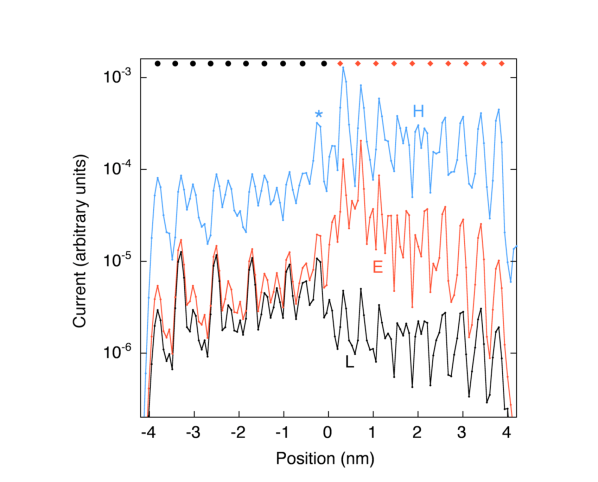
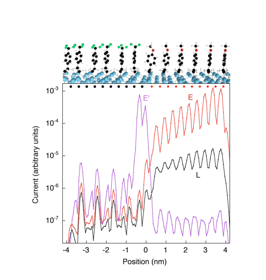
Fig. 5 shows representative results for the calculated current flowing between the tungsten STM tip and silicon substrate via the CF3–styrene/OCH3–styrene chain described in the preceding paragraph at some positive substrate biases (i.e., for empty molecular state imaging) vs. STM tip position along the chain at constant tip height. The corresponding results for negative substrate bias (filled molecular state imaging) are shown in Fig. 6 The black bullets (red diamonds) at the top of each plot indicate the lateral locations of the carbon atoms of the molecular CF3 groups (O atoms of the OCH3 groups).
In both figures, curves L (black) are calculated current profiles along the molecular chain in the very low bias Regime 1 introduced in Section III.2: Here the STM tip Fermi level lies between the silicon conduction band edge and the lowest state of the molecular LUMO band in Fig. 5, and between the silicon valence band edge and the highest state of the molecular HOMO band in Fig. 6. The red curves E are in the low bias Regime 2 of Section III.2 where the STM tip Fermi level is slightly above (below) the lowest (highest) molecular LUMO (HOMO) level in Fig. 5 (Fig. 6). The blue curves H are in the higher bias Regime 3 in which the STM tip Fermi level is near the top the lowest molecular LUMO band in Fig. 5 and just below the bottom of the highest molecular HOMO band in Fig. 6.
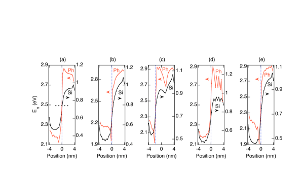
The main features of the current plots in Figs 5 and 6 can be understood qualitatively by considering the profiles along the molecular chain of the calculated electrostatic shifts of the atomic orbital energies defined by Eqn.(1) that enter into the present model as discussed in Section III.1. The relevant information is summarized in Fig. 7 (a). There the red curve (Ph) shows the average of over the six carbon atoms of the benzene ring of each molecule (the scale is on the left axis) vs. the lateral position of the center of the ring along the molecular chain. Since the HOMO and LUMO of both the CF3–styrene and OCH3–styrene are located principally on the benzene ring, the red curve is an approximate guide as to how the molecular HOMO and LUMO orbital energies are affected by the electrostatic potentials due to charge transfer between the atoms of this system. The blue dotted vertical line separates the OCH3–styrene part of the chain on the right from the CF3–styrene part on the left. The black curve labeled Si (for which the scale is on the right axis) shows for the Si atoms to which the molecules bond.
These electrostatic shifts differ by several tenths of an eV between the OCH3–styrene and the CF3–styrene parts of the molecular chain due to the different signs and magnitudes of the charge transfer between the CF3 and OCH3 substituent groups and the benzene rings of the respective molecules. They result in a further lowering of the HOMO and LUMO of the CF3–styrene relative to those of the OCH3–styrene in addition to that predicted by extended Hückel theory and also a very local band bending of the silicon conduction and valence bands in the immediate vicinity of the molecular chain; the Si band edges are lower in energy near the CF3–styrene chain than near the the OCH3–styrene. The horizontal dotted line in Fig. 7 (a) indicates for surface Si atoms if all molecules are replaced by H atoms bound to the Si; the effect of such (passivating) H atoms on the orbital energies of the surface Si atoms is intermediate between those of OCH3–styrene and CF3–styrene molecules bound to the silicon.
Because of the form of these electrostatic profiles, when the Si substrate is biased positively relative to the STM tip, the Fermi level of the metal tip crosses the Si conduction band edge near the CF3–styrene chain and the LUMO levels of the CF3–styrene before doing so at the OCH3–styrene. Thus the CF3–styrene appears higher than the OCH3–styrene for positive substrate bias. This is seen in the theoretical current plots in Fig. 5 and also experimentally in Fig. 2(c) although, as was discussed in Section II the contrast between the OCH3–styrene and CF3–styrene depends on the unknown microscopic details of the STM tip. As will be discussed in Section V it also depends on the specific conformation of the molecular chain.
The red curve (Ph) in Fig. 7 (a) has a sharp minimum at the third CF3–styrene molecule from the junction with the OCH3–styrene chain. Thus the molecular LUMO level is lowest at that molecule. Therefore as the (positive) substrate bias increases, the Fermi level of the STM tip first crosses a molecular LUMO-derived state in the vicinity of that molecule. The prominent peak centered at the third CF3–styrene molecule in the red current profile E in Fig. 5 thus corresponds to the onset of electron injection from the STM tip into the molecular LUMO band. There is no such feature at this molecule in the black curve L in Fig. 5 (which is at lower bias) because in that case the STM tip Fermi level is still too far away from the molecular LUMO levels for resonant tunneling through those levels to be important; thus the larger electrostatic shift of the third CF3–styrene molecule’s LUMO level does not play a large role here. When the bias is large enough for the STM tip’s Fermi level to have risen to the top of the molecular CF3- styrene LUMO band all of the molecular LUMO orbitals throughout the CF3–styrene chain are transmitting resonantly so that the difference between the third CF3–styrene molecule and the other CF3–styrene molecules has been largely erased in the blue curve H in Fig. 5.
Notice that although the Si band edge is lowered locally around the CF3–styrene molecules (see the black curve in Fig. 7 (a)) so that one may expect the Si to appear higher in that vicinity than elsewhere in empty state STM images, the black curve labelled Si in Fig. 7 (a) does not show a minimum at the third CF3–styrene molecule from the junction, confirming that it is the local electrostatic lowering of the molecular LUMO at that molecule and not the effect of the electric fields at the Si that is responsible for the prominent feature at the third CF3–styrene molecule in the red profile E in Fig. 5.
At the bias voltages considered in Fig. 5 the tip Fermi level is well below the OCH3–styrene LUMO states so that resonant transport via the OCH3–styrene LUMO states is not important and thus there is little contrast between different parts of the OCH3- styrene chain except possibly at the highest bias value shown for the OCH3–styrene molecule that is closest to the CF3–styrene chain.
Notice also that in Fig. 5 the contrast between the CF3–styrene and OCH3–styrene chains decreases markedly with decreasing magnitude of the applied bias. This is because the role of resonant transmission via the molecular levels in the CF3–styrene part of the chain is decreasing rapidly whereas no resonant transmission is involved in conduction via the OCH3–styrene which is therefore less sensitive to the magnitude of the applied bias. This behavior is in qualitative agreement with the experimental data in Fig. 2(c) and (d).
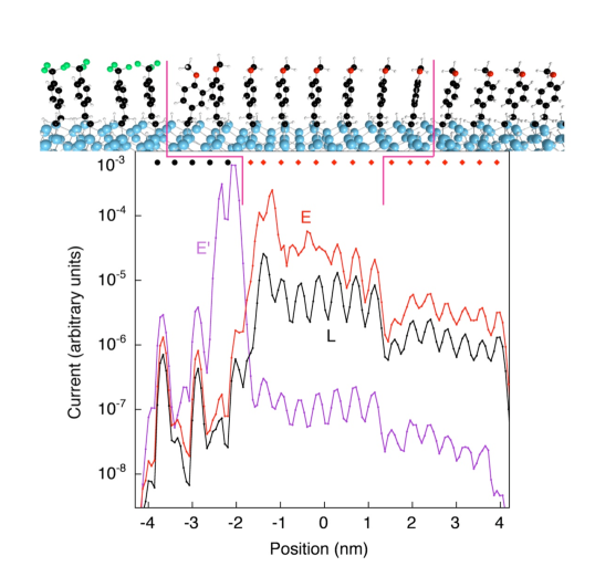
The qualitative features of the theoretical current profiles for negative substrate bias in Fig. 6 can also be understood by considering the electrostatic energy profiles in Fig. 7 (a):
The current profile at very low bias (black curve L, Fig. 6) shows only weak contrast between different parts of the CF3–styrene chain and between different parts of the OCH3–styrene chain because the tip Fermi level is between the silicon valence band edge and the molecular HOMO levels so that resonant tunneling via the molecular HOMO levels (that is strongly modulated by local extrema of the electrostatic potential along the chain of molecular benzene rings exhibited by the red curve in Fig. 7 (a)) is not occurring.lobiasexpt
When the tip Fermi level falls below the highest molecular HOMO-derived level (which is located at and around the second OCH3–styrene molecule from the junction where the electronic electrostatic potential energy [the red curve B in Fig. 7 (a)] has its maximum) the current develops a strong maximum there because of the onset of resonant conduction via the molecular HOMO in that vicinity. This is why the red curve E of Fig. 6 has a strong maximum at the second OCH3–styrene molecule from the junction.
With further increase of the bias voltage the tip Fermi level moves deeper into the molecular HOMO band and resonant transport via molecular states derived from the molecular HOMO becomes possible in other parts of the OCH3–styrene chain as well and thus the peak in the current profile of the OCH3–styrene chain becomes less pronounced, as in the blue curve H in Fig. 6. Notice also that with increasing bias the boundary between the OCH3–styrene and CF3–styrene chains becomes blurred with the higher current typical of the OCH3–styrene chain extending to the nearest one or two CF3–styrene molecules, as in the feature labelled * in the blue curve H in Fig. 6.
Another feature of Fig. 6 is the reversal in the contrast between the OCH3–styrene and CF3–styrene chains between low and intermediate bias: Curve L is higher for the CF3–styrene while curves E and H are higher for the OCH3–styrene. This is possible because the transport mechanisms for the OCH3–styrene in the low and intermediate bias regimes are different: The latter is dominated by resonant conduction via the molecular HOMO levels while the former is not. Whether such a contrast reversal with increasing bias occurs or not was found in the present theoretical study to depend on the structures of the molecular chains: For the geometry shown at the top of Fig. 5 (see also Fig. 4) the OCH3 groups lie especially low relative to the CF3 groups which makes it possible for the CF3–styrene molecules to appear higher than the OCH3–styrene at low negative substrate bias. This occurs despite the fact that both the molecular HOMO levels and the local Si valence band edge are higher in energy on the OCH3–styrene side of the heterowire. For some other geometries of the OCH3–styrene/CF3–styrene chain to be discussed in Section V the OCH3 groups lie higher relative to the CF3 groups and no contrast reversal is found theoretically: The OCH3–styrene appears higher than the CF3–styrene even at low negative substrate bias. In experiment, contrast reversal between the OCH3–styrene and CF3–styrene chains with changing bias was observed in some runs (as in Fig. 2) but not in others (as in Fig. 1), most likely due to undetermined differences between the STM tips involved.
A significant difference between the calculated current profiles in Figs 5 and 6 and our experimental STM height profiles is that the latter do not show the quasiperiodic modulation with a period of roughly two molecular spacings seen in the calculated current profiles for the CF3–styrene part of the chain. This difference can be understood as follows: This quasi-periodic modulation of the calculated CF3–styrene chain current profile is a geometrical effect due to the differing orientations of the CF3 groups and also the associated differing tilts of the molecules along the CF3–styrene chain described near the end of Section IV.1. Therefore it is reasonable to expect this modulation not to be visible in STM images taken at room temperature where the CF3 groups are rotating rapidly about their axes and the local phase of the spatial current modulation is therefore fluctuating rapidly so that only an average over many structures with different phases is observed on the time scale on which the STM scans are recorded, and thus a period equal to the molecular spacing is observed.
IV.3 The current peaks near the CF3–styrene/OCH3–styrene interface
The prominent peaks in the red current profiles E in Figs 5 and 6 near the interface between the CF3–styrene and OCH3–styrene molecular chains have the following important characteristics: The peak for positive substrate bias in Fig. 5 is narrow, just one molecule wide and occurs on the CF3–styrene side of the junction. The peak at negative substrate bias in Fig. 6 is broader, extending over a few molecules and occurs on the OCH3–styrene side of the junction. These properties of the interfacial peak at negative substrate bias are consistent with the experimental data presented in Section II. Furthermore the interfacial peak at negative substrate bias was seen experimentally at low bias in all of the many CF3–styrene/OCH3–styrene heterojunctions that we imaged and persisted when the STM tip changed spontaneously in the course of the imaging. By contrast, in empty state imaging (i.e., for positive substrate bias), no discernible height enhancement at the interface was usually observed.
The above discussion in Section IV.2 identified the interfacial peaks in the calculated current profiles as being due to a maximum or minimum of the electrostatic contribution to the molecular HOMO or LUMO energy along the molecular chain occurring at the location of the peak. However, in order to understand the physics underlying the differences between the predicted properties of the peaks at positive and negative substrate bias and the similarities and differences between the predictions and experiment it is necessary to examine how these features of the current profiles depend on the structure of the molecular chain. This will be explored in the next section.
V Relationship between structure, electrostatics and current profiles
Several significant aspects of the structures of the experimentally realized molecular chains such as whether the molecules are tethered to the Si in the T or D orientation (as defined in Section III.3) and whether the OCH3 groups are T or D oriented, are not obvious from a direct inspection of the experimental STM images. It is also not clear theoretically which types of these structures should be favoured by the kinetics of the growth process or by energetics at room temperature. Thus it is desirable to study a variety of plausible relaxed molecular chain geometries theoretically and to clarify how their structures relate to their electrostatic and current profiles. This is done in the present Section and the results presented here also elucidate the mechanisms underlying the phenomena described in Sections II and IV. Potential energy profiles were calculated for many relaxed chain geometries and a few representative examples will be discussed below, along with possible experimental implications.
V.1 Notation
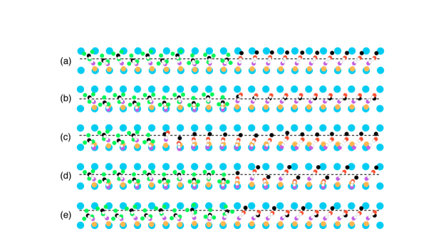
The important features of these molecular chain geometries are summarized in Fig. 8 where projections of the positions of some key atoms of the molecular chains onto the Si (001) plane are shown: Each panel in Fig. 8 shows two rows of Si surface atoms belonging to different Si dimer rows. In each case the molecules are tethered to the lower row of Si atoms. The C atoms that bond to the Si atoms are orange. The C atoms that bond to the C atoms that bond to the Si atoms are violet. The C atoms of the CF3 and OCH3 groups are black. The O atoms are red and the F atoms are green. The C atoms belonging to the benzene rings that bond to O atoms or to C atoms not belonging to the benzene rings are white. The other other C atoms of the benzene rings, the H atoms and the other Si atoms are not shown for clarity. The dashed line shows the path of the tip atom of the STM for the theoretical STM current profiles for each structure that are presented in this paper.
The structure considered in Section IV will henceforth be referred to as “Structure (a)” as per its label in Fig. 8. The other structures to be discussed here will be referred to similarly, according to their labelling in Fig. 8. Each of these structures consists of 20 molecules taken from the central region of a relaxed 40 molecule chain without further relaxation, as described at the end of Section III.1.
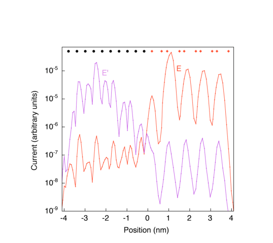
V.2 Structure (b)
In Structure (b), as in Structure (a), the OCH3–styrene molecules are tethered to the Si in the T orientation. But the OCH3 groups are approximately reversed relative to Structure (a) and are now in the D orientation (defined in Section III.3). In Structure (b) the tethering of the CF3–styrene molecules to the Si alternates between T and D and the orientation of the F atoms in the CF3 groups also alternates from molecule to molecule. However since this is a relaxed structure neither the OCH3–styrene chain nor the CF3–styrene chain has a truly periodic geometry.
V.2.1 Electrostatic and current profiles
The electrostatic potential energy profiles along the chain of benzene rings and along the row of Si atoms to which the molecules of Structure (b) bond are the red and black curves in Fig. 7(b), resp. Some representative current profiles for Structure (b) calculated at constant tip height along the dashed line in Fig. 8(b) are shown in Fig. 9 together with a side view of a part of this molecular chain. The qualitative behavior of the calculated current profiles in Fig. 9 can be understood by considering the features of the potential energy profile along the chain of benzene rings in Fig. 7(b) and applying reasoning analogous to that in Section IV.2: The current profile under a moderately low positive substrate bias for which the STM tip Fermi level is just above the lowest level of the molecular LUMO band (the violet curve E′) has a strong maximum one molecule wide at the CF3–styrene molecule next to the OCH3–styrene chain where the benzene ring potential energy profile has its sharp minimum. The current profile under a moderately low negative substrate bias for which the STM tip Fermi level is just below the highest level of the molecular HOMO band (the red curve E) rises gradually to a broad maximum at the end of the OCH3–styrene chain remote from the CF3–styrene where the benzene ring potential energy profile has its broad maximum. Unlike in Fig.6, in this case there is no contrast reversal between the OCH3–styrene and CF3–styrene chains with increasing negative substrate bias; the OCH3–styrene is higher in both the very low bias profile L and the moderately low bias profile E. This is because the OCH3 group is located higher relative to the CF3 group in Structure (b) than in Structure (a).
V.2.2 Significance of the results
The two main differences between the electrostatic profiles for Structure (b) and those for Structure (a) (shown in Fig. 7(b) and Fig. 7(a)) are:
1. The minimum of the benzene ring electronic potential energy profile (while remaining very sharp) has shifted from the third CF3–styrene molecule from the heterojunction in Fig. 7(a) to the CF3–styrene molecule next to the heterojunction in Fig. 7(b).
2. The maximum of the benzene ring potential energy profile while remaining broad has shifted from the vicinity of the heterojunction (on the OCH3–styrene side) in Fig. 7(a) to the vicinity of the end of the OCH3–styrene chain that is remote from the heterojunction in in Fig. 7(b).
Systematic studies of various structures and their potential energy profiles showed the reversal of the slope of the potential energy profile along most the chain of benzene rings of the OCH3–styrene chain from Structure (a) to Structure (b) in Fig. 7 should be attributed not to the OCH3 groups being switched from the T to the D orientation per se, but primarily to the fact that the projection onto the axis of the molecular chain of the dipole moment associated internal charge structures of the OCH3 groups (negative O and positive CH3) has reversed direction from Structure (a) to Structure (b) as is evident from the geometries of the two structures in Fig. 8. This reversal of the charge structure along the molecular axis should lead to a reversal of the slope of the potential energy profile and this is what is in fact seen in Fig. 7.
In this way the change in the geometrical structure of the OCH3–styrene chain has resulted in the shift of the potential energy maximum (and STM tip current maximum at moderately low negative substrate bias) from the vicinity of the heterojunction to the vicinity of the far end of the OCH3–styrene chain.
An important point to note is that because of the geometrical structure of the OCH3–styrene molecules and the way in which they bond to the silicon the internal dipole moment of the OCH3 group has a strong component parallel to the silicon surface and the OCH3 groups of all of the OCH3–styrene molecules can be aligned in such a way that the projections of the OCH3 groups of all of these molecules onto the axis of the molecular chain have the same sign. This results in a gradual buildup of the electrostatic potential along the OCH3–styrene chain and a broad electrostatic potential energy peak near one of its ends as in Fig. 7(a) or (b), and consequently a broad current peak under moderately low negative substrate bias, consistent with the experimental results presented in Section II.
By contrast, because the geometrical orientation of the CF3 group (see Fig. 4) and the arrangement of charges within it are different than for the OCH3 group, and because of the repulsion between the F atoms on different molecules (see the end of Section IV.1), such a well ordered arrangement of dipole projections onto the axis of the molecular chain does not occur for the CF3–styrene chain. Thus the electrostatic potential energy minimum on the CF3–styrene side of the heterojunction is a much more local phenomenon. Its location is determined by the orientations of a few molecules surrounding it and by the fringing electrostatic field of the OCH3–styrene chain that extends across the heterojunction into the CF3–styrene chain. Thus the electrostatic potential energy minimum on the CF3–styrene side of the heterojunction is very narrow and its location is sensitive to the details of the local molecular geometry. It is therefore reasonable to expect any profile peak associated with it in STM imaging at room temperature (at positive substrate bias), if present at all, to be more strongly impacted by thermal fluctuations in the molecular geometry and therefore less readily observed than the corresponding peak at negative substrate bias on the OCH3–styrene side of the molecular chain. This is consistent with the differences between the experimental results obtained under positive and negative substrate bias that are presented in Section II.
Experimentally, height enhancement was observed in the STM images towards the end of the OCH3–styrene chain that is far from the junction with the CF3–styrene at low negative substrate bias as can be seen, for example, in Fig. 1(d). Because in this work the growth of the OCH3–styrene chain followed the growth of the CF3–styrene, a charged dangling bond is normally expected to be present at the end of the OCH3–styrene chain (remote from the OCH3–styrene/CF3–styrene junction) where the growth of the molecular chain terminated, as in previous experimental work on styrene chains on silicon.Lopinski ; Nature The electrostatic potential due to this charged dangling bond gives rise to enhancement of the height profile of the molecular chain in its vicinity in STM experiments as is discussed in Ref.Nature, If alignment of OCH3–styrene molecular dipoles as in Structure (b) was occurring in the present experiments, the associated electrostatic profiles such as in Fig. 7(b) would also contribute to enhanced current near the end of the molecular chain as in curve E in Fig. 9, and hence to the enhanced height profile there in constant current STM experiments as in Fig. 1(d). Determining experimentally whether such a molecular dipole contribution to the height profile in vicinity of the dangling bond is present or not is in principle possible by passivating the dangling bond through the addition of a H atom and observing whether any height enhancement remains afterwards near the end of OCH3–styrene chain. Carrying out such a test was beyond the scope of the present experimental work. However, the fact that height enhancement was consistently observed experimentally near the OCH3–styrene/CF3–styrene heterojunction at low negative substrate bias suggests that OCH3–styrene chains with dipole fields similar to that arising from Structure (a) rather than Structure (b) in Fig. 8 played the dominant role in these experiments.
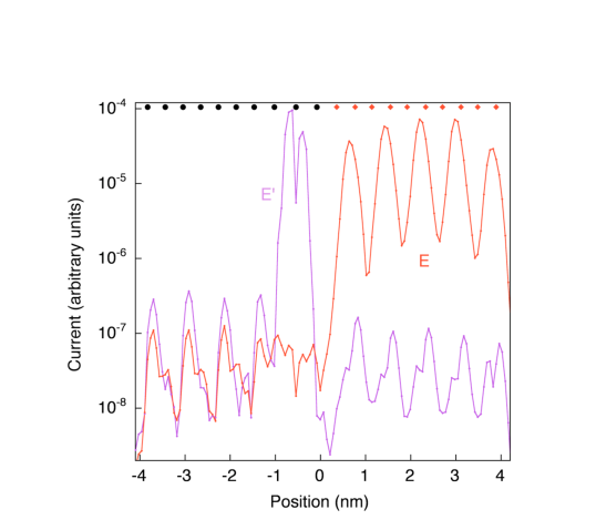
V.3 Structure (c)
Structure (c) consists of 5 CF3–styrene and 15 OCH3–styrene molecules. The geometry of the CF3–styrene molecules and of the OCH3–styrene molecule that is next to the CF3–styrene is similar to that of the corresponding molecules in Structure (b). However, as can be seen in Fig. 8(c), the other OCH3–styrene molecules in Structure (c) have a different geometry: they are tethered to the Si in the D orientation and their OCH3 groups are in the T orientation. Between the 8th and 9th OCH3–styrene the molecules from the junction with the CF3–styrene there is another abrupt change in the molecular geometry: Although the molecules to the right and left of this dislocation are both D-tethered and the OCH3’s are T oriented, the molecules to the right of the fault tilt more to the right and their OCH3 groups are oriented nearly perpendicularly to the axis of the molecular chain.
This is reflected in the electrostatic potential energy profile along the chain that is plotted in Fig. 7(c): Since the molecular structure at the junction is similar to that for Structure (b) the potential profile on the benzene rings is also similar there, i.e., there is a sharp potential energy minimum at the CF3–styrene molecule at the junction. Since for OCH3–styrene molecules 2-8 from the junction the orientation of the O and two C atoms bonded to it is similar to that for the OCH3–styrene molecules in Structure (a) the orientation of the relevant dipoles on that part of the chain is also similar and thus the potential energy profile is also qualitatively similar: There is a broad potential energy maximum on the OCH3–styrene benzene rings peaked near the junction with the CF3–styrene. However, the different orientation of the charged groups of the of the 9th-15th OCH3–styrene molecules from the junction results in a reversal of the slope of the potential profile and the electronic potential energy on the OCH3–styrene benzene rings rises to another maximum near the right hand end of the molecular chain.
The calculated STM current profiles for Structure (c) shown in Fig. 10 are again consistent with the potential energy profile along the chain of benzene rings: At moderately low positive substrate bias (violet curve E′) the current profile has a sharp maximum one molecule wide at the CF3–styrene molecule where the potential energy minimum along the molecular chain is located. At moderately low negative substrate bias (red curve E) there is a broad current maximum peaked on the OCH3–styrene side of the junction where the potential energy has one of its maxima. From there the current falls off to a minimum near the middle of the OCH3–styrene chain where the potential energy curve also has its minimum. To the right of this minimum both the potential energy and current rise again but the current does not rise as high as near the junction and then begins to fall off again. This difference is due to the fact that for the red curve E the electron transmission through the molecules has not quite reached resonance for the OCH3–styrene HOMOs at the right end of the OCH3–styrene chain (although it has done this for the OCH3–styrene near the junction) and also because the OCH3–styrene molecules are tilted more at the right end of the chain than at the left. This geometrical difference also shows up as a step in the other current profiles in Fig. 10 at the dislocation in the OCH3–styrene chain.
For Structure (c) there is again no reversal of the contrast between OCH3–styrene and CF3–styrene chains with increasing bias.
V.4 Structure (d)
In Structure (d) the geometry of the CF3–styrene chain is broadly similar to those of Structures (b) and (c). However, in the OCH3–styrene chain the tethering to the Si alternates between D and T. The orientation of the OCH3 groups is all T and most of the relevant OC dipoles are oriented roughly as for Structure (a). Thus one should expect a potential energy profile along the chain of OCH3–styrene benzene rings somewhat similar to that for Structure (a). Indeed the red curve in Fig. 7(d) does have its maximum in the OCH3–styrene chain near the junction with the CF3–styrene and it declines overall to the right, but the decline is modulated by strong oscillations due to the different tethering of alternate OCH3–styrene molecules to the Si. The potential energy profile along the chain of benzene rings on the CF3–styrene chain of Structure (d) is quite different than that for Structures (b) and (c): There is no potential energy minimum on the CF3–styrene next to the junction but instead a shallow minimum near the middle of the CF3–styrene chain.
The current profiles for Structure (d) are shown in Fig. 11 for moderately low positive substrate bias (violet curve E′) and moderately low negative substrate bias (red curve E). Again the maxima of these profiles are near the lowest and highest points of the potential energy profile along the chain of benzene rings, respectively. But in this case the potential energy peak in the OCH3–styrene chain is less prominent and narrower than in the the previously discussed cases due to the less uniform structure of the array of dipoles. The broad potential energy minimum in the CF3–styrene results in a broader current peak at positive substrate bias than in the cases discussed earlier.
This illustrates further the strong sensitivity of the CF3–styrene chain’s potential minima to the precise details of the conformation of a single molecule or a few molecules: In Structure (d) the OCH3–styrene molecule at the junction of the chains is D-tethered and the OCH3 group is T oriented while the reverse is true for Structures (b) and (c) while the CF3 groups are rotated slightly differently and CF3–styrene at the junction tilts somewhat differently.
V.5 Structure (e)
Structure (e) is similar to Structure (a) except that now the orientations of the OCH3 groups alternate between T and D and the CF3 groups have rotated about their axes through substantial angles. Because of the alternating orientations of the OCH3 groups the electric fields due to the different OCH3–styrene molecules are not aligned and produce a potential energy profile in Fig. 7(e) with a very broad maximum near the end of the chain remote from the junction. The different orientations of the CF3 groups than in Structure (a) result in a sharp potential energy minimum at the second CF3–styrene molecule from the junction.
The current profiles for Structure (e) are shown in Fig. 12 for moderately low positive substrate bias (violet curve E′) and moderately low negative substrate bias (red curve E). As expected for such a potential energy profile we see a strong narrow current peak on the second CF3–styrene molecule from the junction. The broad potential energy maximum on the OCH3–styrene chain produces a broad current maximum peaked towards the end of the OCH3–styrene chain that is remote from the junction at intermediate negative substrate bias.
For both Structure (e) and Structure (d) the alternating geometries along the OCH3–styrene chains result in a strong modulation of the current with a period of 2 molecular spacings. Since this modulation is not seen experimentally, either these structures are not realized in the experiments or the experiments are averaging over geometries for which the modulation occurs with different phases due to thermal fluctuations of the molecular geometries at room temperature.
VI Electrostatic vs. Electronic Molecule-Molecule Coupling
For comparison, similar calculations to those described above were also carried out for Structure (a)
(i) omitting the environmental electrostatic shifts of atomic orbital energies defined by Eqn. 1. No enhancement of the current near the heterojunction (such as in curves E in Fig. 5 and 6) was found in those calculations.
(ii)Transport calculations were also carried out including the electrostatic shifts but with all Hamiltonian matrix elements and basis function overlaps responsible for direct electronic hopping from molecule to molecule switched off. These calculations produced very similar current profiles along the molecular chain to those in Fig. 5 and 6, including the interface current peaks and even the feature labelled in the blue curve H in Fig. 6. However these features appeared at somewhat different values of the bias voltages because the molecular HOMO and LUMO bands are narrower (as expected) when the inter-molecule Hamiltonian matrix elements and basis state overlaps are turned off.
These results confirm that the enhanced current features near the interface in Fig. 5 and 6 result from electrostatic fields established by the polar molecules. These results therefore suggest an electrostatic origin for the filled-state interfacial enhancement resolved experimentally in Fig. 1 and 2 at low bias. (Significantly, no such interfacial current enhancement was observed experimentallystymeth in styrene/methylstyrene heterostructures on Si where molecular electric fields are expected to be much weaker because of the weaker charge transfer within those molecules.)
Furthermore, although electronic hopping from molecule to molecule may be occurring quite efficiently in substituted styrene chains on Si(100) as is discussed in Ref. stymeth, , these calculations demonstrate the hopping not to be necessary for the occurrence of the interfacial features reported in the present work.
VII Modeling Single-Triple row CF3–styrene Heterostructures and their influence on conduction through the underlying Silicon
The main features of the calculated current profiles of the molecular heterostructures modeled theoretically in the preceding sections derive directly from the electronic structures of the molecules themselves modulated by the electrostatic fields due to other nearby molecules. This however is not the case for the most striking feature of the experimental data shown Fig. 3(d) and (e) where at low negative substrate bias the electric current passing through a triple row of CF3–styrene molecules is strongly depressed relative to that passing through the nearby single row of CF3–styrene molecules. Our theoretical findings presented below suggest that the influence of the adsorbed CF3–styrene molecules on the electrostatic potential in the underlying silicon may be responsible for this phenomenon.
Representative results of our calculations are presented in Fig. 13. The molecular geometry studied is shown schematically in Fig.13(a). In the model considered the long CF3–styrene line is located between the two short ones to minimise sensitivity to the Si cluster edges. All of the molecules are assumed to be tethered to the silicon in the T orientation defined in Section III.3 and shown in Fig. 4(b). Fig.13(b) shows the simulated constant height current along the long (central) CF3-styrene line. At low negative substrate bias (for which the STM tip Fermi level is close to the silicon valence band edge), the calculated current (curve V) drops by a factor of 26 from the tallest current peak near the left hand end of the single CF3-styrene line to the tallest peak near the right hand end of the central line of the triple CF3-styrene structure. The origin of this effect is seen in the solid black curve labeled “Si” in Fig.13(c): Dipole fields associated with the CF3-styrene molecules lower the Si orbital energies below the triple CF3-styrene by 0.2eV more than under the single file CF3-styrene. At low bias this reduces the silicon electronic density of states near the silicon surface at the Fermi level of the STM tip more under the triple CF3-styrene line than under the single CF3-styrene line, resulting in the weaker tip current through the former. As the magnitude of the bias increases eventually the tip Fermi level is lowered further by an amount substantially exceeding the differential electrostatic energy shift between the Si orbitals under the triple and single CF3-styrene lines and thus the contrast between the STM tip currents through the triple and single CF3-styrene lines becomes weaker as is seen in curve L of Fig.13(b) for which the tip Fermi level is 0.5eV lower than for curve V.
This behavior found in the simulations (lower current through the triple CF3-styrene line than through the single CF3-styrene line at low bias and the reduction in this contrast with increasing magnitude of the bias) is qualitatively similar to that seen experimentally in Fig. 3(e). However, quantitatively the suppression of the current through the triple CF3-styrene line at low bias is more pronounced in the experiment (Fig. 3(e)) than in the theoretical curve V of Fig.13(b): A 0.2-0.3nm difference in tip height at constant current (as between the triple and single CF3-styrene lines in Fig. 3(e) at low bias) normally corresponds to approximately a 2-3 orders of magnitude change in current at constant tip height in STM experiments.
Part of this difference between the simulation and experiment may be due to the unknown microscopic details of the STM tip, which are known to influence the height contrast between CF3-styrene and OCH3-styrene lines as is discussed in Section II and can be seen in Fig.2. However, the limited size of the model system for which the present simulations could be carried outsize is clearly responsible for at least a part of the difference between the experimental and theoretical findings: While the downward electrostatic shift of the Si orbital energies (as indicated by the solid black curve in Fig.13(c)) is clearly larger under the triple than the single CF3-styrene line, it is evident that the 8 molecule single CF3-styrene line modeled is not long enough for the electrostatic potential in the silicon under the single CF3-styrene line to reach a plateau with increasing distance from the junction with the triple CF3-styrene line, i.e., the electrostatic influence of the triple row of molecular dipoles of the triple CF3-styrene line is clearly being strongly felt under much of the single CF3-styrene line as well, resulting in diminished contrast in the calculated current between the single and triple CF3-styrene lines relative to that which may be expected in larger model systems. In this regard it is instructive to compare the electrostatic profile in the silicon under the single-triple CF3-styrene heterostructure with that for a somewhat longer single file CF3-styrene/OCH3-styrene heterostructure shown by the dashed black curve in Fig.13(c): For the latter heterostructure the potential profile in the silicon under the CF3-styrene line (which is on the left) does show a pronounced plateau where the value of the electrostatic potential is close to that for the single-triple CF3-styrene heterostructure under the end of the single CF3-styrene line that is furthest from the triple CF3-styrene line.
In comparing theory with experiment it is noted that there is also contrast between the tip currents calculated for tip positions over the three molecular rows within the triple row structure: The calculated current for the tip over the leftmost molecular row in Fig.13(a) for the same tip height and bias as for plot V of Fig.13(b) is shown by the dashed curve at the bottom of Fig.13(b): The current over the left molecular row is smaller than over the center row of the triple structure (plot V). The calculated current over the rightmost row of Fig.13(a) (not shown) is intermediate between that for the left and center rows. These results suggest that stronger contrast between the single CF3-styrene line and parts of the triple CF3-styrene than is seen in plot V of Fig.13(b) may be possible theoretically. However, calculations for larger silicon clusters than were feasible in this study are required to eliminate possible cluster edge effects and develop a better understanding of this issue.
If the magnitude of the negative substrate bias is increased still further, well beyond that for current plot L in Fig.13(b), the STM current through the single CF3-styrene line is predicted by the present simulation to begin to increase more rapidly than that through the central line of the triple CF3-styrene structure. This is seen in curve H of Fig.13(b) where the current through the single CF3-styrene line is again much larger than that through the triple CF3-styrene line. This effect can be understood by considering the red curve (Ph) in Fig.13(c): This shows the average of over the six carbon atoms of the benzene ring of each molecule of the long CF3-styrene row. This is higher for the single CF3-styrene line than for the triple CF3-styrene line. Therefore the molecular HOMO levels for the molecules in the single CF3-styrene line are higher in energy than those for molecules in the center row of the triple CF3-styrene line. Consequently the molecular HOMO levels for the molecules in the single CF3-styrene line are crossed by the Fermi level of the STM tip at lower magnitudes of the negative substrate bias than for molecules in the triple CF3-styrene line which results in the renewed enhancement of the current through the single CF3-styrene line relative to the triple CF3-styrene line seen in curve H of Fig.13(b). No recovery of stronger contrast between the single and triple CF3-styrene lines at stronger negative substrate bias is seen experimentally in Fig. 3(e) indicating that even for the strongest negative substrate bias values realized in these experiments the STM tip Fermi level remains well above the CF3-styrene HOMO levels even for the molecules in the single CF3-styrene line. This is consistent with our experimental findings for the CF3-styrene/OCH3-styrene heterostructures where no acceleration of the increase of the apparent height of the CF3-styrene with bias at strong negative substrate bias (that would be indicative of the STM tip Fermi level crossing the CF3-styrene HOMO) was observed.
VIII Discussion
The present experimental and theoretical work has begun to explore how electric fields emanating from molecules influence electrical conduction through other molecules in their close vicinity and in the underlying substrate.
In this work we have employed density functional calculations only to estimate the electrostatic potential throughout the system in its electronic ground state, an application of density functional theory that is believed to be soundly based at the fundamental level. The phenomena that we report on here can be understood qualitatively by considering just the results of these electrostatic calculations as summarized in Fig. 7 and 13(c). Transport calculations are however necessary to translate the electrostatics into current profiles that can be compared with the experimental STM data. As is discussed in Section III.1, transport calculations that incorporate electronic structures obtained entirely from density functional theory, although popular, are not soundly based and are often misleading, especially for molecules on semiconductors. We therefore base our transport calculations instead on electronic structures obtained from semi-empirical tight binding models modified to include the density functional theory-based ground state electrostatic potentials.
Our theoretical modeling indicates the observed low bias filled-state current enhancement in the interfacial OCH3-styrene molecules to be due to the collective effect of the electric dipole fields generated by the OCH3 groups of the OCH3–styrene chain when the OCH3 groups are aligned preferentially so that their carbon atoms are further from the heterojunction than their oxygen atoms, as they are, for example, in Fig. 8(a). It is plausible that structures of this sort are prevalent in these systems since some of them should be favored for molecules subject to a weak net mutual steric repulsion as is discussed Section IV.1. However the resolution of our experimental STM data which was taken at room temperature is not sufficient to determine independently whether or not the molecular chains have structural order of this sort. Furthermore it is apparent from a comparison of our experimental data and theoretical results that the CF3 groups in the CF3–styrene molecules must be spinning rapidly enough on their axes that only an average over many conformations of these molecules is being observed in the STM images. Similarly it seems possible that many conformations of the OCH3–styrene molecules are being averaged over rapidly in the STM imaging and that the above alignment of the OCH3 groups is simply more commonly present than other structures, such as that in Fig. 8(b) for which the apparent height enhancement should be near the end of the OCH3–styrene chain that is remote from the junction.
The behavior of the imaging height enhancement that we observe experimentally with increasing negative substrate bias is also consistent with the predictions of our theoretical model of this phenomenon.
Under positive substrate bias simulations indicate that height enhancement near the junction should also occur but should in this case be confined to only a single molecule. The location of the predicted height enhancement under positive substrate bias is sensitive to the details of the local molecular geometry in its vicinity that are expected to fluctuate rapidly at room temperature. Thus definitive observation of this effect will most likely require cryogenic experimental work.
The work reported here has succeeded in identifying transport phenomena occurring at molecular length scales that can reasonably be attributed to electric fields emanating from polar molecules impinging on other nearby molecules and on the underlying substrate, and in developing some insights into the detailed physical mechanisms that may be involved. As has been discussed in Section I these phenomena may ultimately find device applications, such as molecular switches in which the current through a molecule is switched by conformational changes in another nearby molecule and/or devices in which conduction through a semiconductor substrate is controlled with the help of molecules at its surface.
However further experimental and theoretical work is needed in order to better understand and ultimately control such phenomena.
Acknowledgments
This research was supported by the Canadian Institute for Advanced Research, NSERC, iCORE and the NRC. PGP wishes to thank NRC-INMS for support. Some numerical computations presented in this work were performed on WestGrid computing resources, which are funded in part by the Canada Foundation for Innovation, Alberta Innovation and Science, BC Advanced Education, and the participating research institutions. WestGrid equipment is provided by IBM, Hewlett Packard, and SGI. We have benefited from discussions with G. DiLabio and from the technical expertise of D. J. Moffatt and M. Cloutier.
References
- (1) A. Troisi and M. A. Ratner, Small 2, 172 (2006).
- (2) N. J. Tao, Nature Nanotechnology 1, 173 (2006).
- (3) G. Kirczenow, Molecular Nanowires and their Properties as Electrical Conductors in The Oxford Handbook of Nanoscience and Technology edited by A. V. Narlikar and Y. Y. Fu, Oxford University Press, U.K. (2009) in press.
- (4) L. Venkataraman, J. E. Klare, C. Nuckolls, M. S. Hybertsen and M. L. Steigerwald Nature 442, 904 (2006)
- (5) L. Venkataraman, Y.S. Park, A.C. Whalley, C. Nuckolls, M.S. Hybertsen, M.L. Steigerwald, Nano Lett. 7, 502 (2007).
- (6) P.G. Piva, G.A. DiLabio, J.L. Pitters, J. Zikovsky, M. Rezeq, S. Dogel, W.A. Hofer, R.A. Wolkow, Nature 435, 658 (2005).
- (7) K.R. Harikumar, J.C. Polanyi, P.A. Sloan, S. Ayissi, W.A. Hofer, J. Am. Chem. Soc. 128, 16791 (2006).
- (8) A preliminary account of some of the present findings has been presented elsewhere: P.G. Piva, R.A. Wolkow and G. Kirczenow, Phys. Rev. Lett. 101, 106801 (2008)
- (9) G. P. Lopinski, D.D.M. Wayner, R.A. Wolkow, Nature 406, 48 (2000).
- (10) P. Delaney and J. C. Greer, Phys. Rev. Lett. 93, 036805 (2004).
- (11) N. Sai, M. Zwolak, G. Vignale and M. Di Ventra, Phys. Rev. Lett. 94, 186810 (2005).
- (12) C. Toher, A. Filippetti, S. Sanvito and K. Burke Phys. Rev. Lett. 95, 146402 (2005).
- (13) P. Darancet, A. Ferretti, D. Mayou, and V. Olevano, Phys. Rev. B75, 075102 (2007).
- (14) F. Evers and K. Burke, Nano and Molecular Electronics Handbook p. 24-1 (Ed. S. E. Lyshevski) Taylor & Francis, Boca Raton, (2007). Prejudice etc
- (15) S. H. Ke, H. U. Baranger and W. T. Yang, J. Chem. Phys. 126, 201102 (2007).
- (16) C. D. Pemmaraju, T. Archer, D. Sánchez-Portal and S. Sanvito Phys. Rev. B75, 045101 (2007).
- (17) E. Prodan and R. Car, Phys. Rev. B76, 115102 (2007). TDDFT
- (18) S. Y. Quek, J. B. Neaton, M. S. Hybertsen, E. Kaxiras and S. G. Louie, Phys. Rev. Lett. 98, 066807 (2007).
- (19) M. Koentopp, C. Chang, K. Burke and R. Car, J. Phys.: Condens. Matter 20, 083203 (2008) and references therein.
- (20) K. S. Thygesen and A. Rubio, J. Chem. Phys. 126, 091101 (2007); Phys. Rev. B77, 115333 (2008).
- (21) C. Toher and S. Sanvito, Phys. Rev. Lett. 99, 056801 (2007); Phys. Rev. B77, 155402 (2008).
- (22) K. S. Thygesen, Phys. Rev. Lett. 100, 166804 (2008).
- (23) P. Hohenberg, and W. Kohn, Phys. Rev. 136, B864 (1964).
- (24) P. E. Kornilovitch, A. M. Bratkovsky, R.S. Williams, Phys. Rev. B 66, 245413 (2002).
- (25) E. G. Emberly and G. Kirczenow, Phys. Rev. Lett. 91, 188301 (2003).
- (26) A. Troisi and M. A. Ratner, Nano Letters 4, 591 (2004).
- (27) J. J. de Jonge, M. A. Ratner, S. W. de Leeuw, J. Phys. Chem. C 111, 3770 (2007).
- (28) J. J. Boland, Surf. Sci. 261, 17 (1992).
- (29) G.A. DiLabio, P.G. Piva, P. Kruse, and R.A. Wolkow, J. Am. Chem. Soc. 126, 16048 (2004).
- (30) X. Tong, G.A. DiLabio, O.J. Clarkin, and R.A. Wolkow, Nano Lett. 4, 357 (2004).
- (31) P. Kruse, E.R. Johnson, G.A. DiLabio, and R.A. Wolkow, Nano Lett. 2, 807 (2002).
- (32) P.G. Piva, unpublished.
- (33) Certain substituents have been found to hinder the line growth process, and on occasion successful heterowire formation has been observed to depend on deposition sequence.
- (34) L.P. Hammett, J. Am. Chem. Soc. 59, 96 (1937).
- (35) G.A. DiLabio, D.A. Pratt, J.S. Wright, Chem. Phys. Lett. 311, 215 (1999) and references therein.
- (36) A. Y. Anagaw, R. A. Wolkow, G. A. DiLabio, J. Phys. Chem. C112, 3780 (2008).
- (37) H. Raza, K. H. Bevan, D. Kienle, Phys. Rev. B 77, 035432 (2008).
- (38) G. Kirczenow, P. G. Piva and R. A. Wolkow, Phys. Rev. B 72, 245306, (2005).
- (39) D.M. Cyr, B. Venkataraman, G.W. Flynn, A. Black and G.M. Whitesides, J. Phys. Chem., 100, 13747 (1996).
- (40) J.R. Hahn, W. Ho, Phys. Rev. Lett. 87, 196102 (2001).
- (41) W. Kohn and L.J. Sham, Phys. Rev. 140, A1133 (1965).
- (42) J. Buker and G. Kirczenow, Phys. Rev. B78, 125107 (2008).
- (43) T. Rakshit, G.-C. Liang, A.W. Ghosh, and S. Datta, Nano Letters 4, 1803 (2004).
- (44) K. H. Bevan, F. Zahid, D. Kienle, and H. Guo, Phys. Rev. B 76, 045325 (2007).
- (45) R. Hoffman, J. Chem. Phys. 39, 1397 (1963).
- (46) J. H. Ammeter, H.-B. Bürgi, J. C. Thibeault, and R. Hoffman, J. Am. Chem. Soc. 100, 3686 (1978) implemented in the YAeHMOP numerical package by G. A. Landrum and W. V. Glassey.
- (47) S. Datta, W. Tian, S. Hong, R. Reifenberger, J. I. Henderson, C. P. Kubiak, Phys. Rev. Lett. 79, 2530 (1997).
- (48) E. G. Emberly and G. Kirczenow, Phys. Rev. Lett. 87, 269701 (2001).
- (49) E. G. Emberly and G. Kirczenow, Phys. Rev. B 64, 235412 (2001).
- (50) J. G. Kushmerick, D. B. Holt, J. C. Yang, J. Naciri, M. H. Moore, R. Shashidhar, Phys. Rev. Lett 89, 086802 (2002).
- (51) D. M. Cardamone and G. Kirczenow, Phys. Rev. B77, 165403, (2008); AIP Conf. Proc. 995, 135 (2008).
- (52) J. Cerdá and F. Soria, Phys. Rev. B 61, 7965 (2000)
- (53) D. Kienle, K. H. Bevan, G. -C. Liang, L. Siddiqui, J. I. Cerdá and A. W. J. Ghosh, Appl. Phys. 100, 04371 (2006)
- (54) The Gaussian03 package with the B3PW91 density functional and Lanl2DZ basis set was used.
- (55) E. G. Emberly, G. Kirczenow, Chem. Phys. 281, 311 (2002), Appendix A.
- (56) The temperature in the Fermi functions was set to 0 in the calculations reported here.
- (57) The numerical implementation of the Gaussian98 package was used.
- (58) See the inset of Fig.1d of Ref.brief, for a representative example of the calculated densities of states of the HOMO bands for the OCH3- styrene and CF3–styrene molecules in a OCH3–styrene/CF3–styrene heterostructure on silicon.
- (59) J.-H. Cho, D.-H. Oh, and L. Kleinman,Phys. Rev. B 65, 081310(R) (2002).
- (60) Image made with MacMolPlot program of B. M. Bode, M. S. Gordon, J. Mol. Graphics and Modeling 16, 133 (1998).
- (61) In our STM experiments imaging of the CF3–styrene/OCH3–styrene molecular heterowires in this very low bias regime was rarely possible, as is discussed in Section III.2.
- (62) Plots L and V in Fig. 4(b) of Ref. brief, are at the same values of the bias but for a tip trajectory 0.1nm lower that in Fig. 13(b) of the present article. The lateral location of the tip trajectory for plots L,V and H in Fig. 13(b) was chosen so as to maximize the calculated current along the (straight line) trajectory in plot L in both the single and triple molecular chain regions in order to accurately reflect the current contrast between different parts of the trajectory. Such optimization was not carried out in Fig. 4(b) of Ref. brief, .
- (63) We include 423 Si atoms and 936 other atoms in our density functional calculations of the electrostatic potentials in the single-triple row CF3–styrene heterostructure on silicon.