Coherent interference effects in a nano-assembled optical cavity-QED system
Fano resonancesref:Fano1 , the signature of multi-path interference between a continuum and discrete resonance, have been exploited in opticsref:Wood1 ; ref:Fan5 for a variety of applications including biosensingref:Chao1 , optical switchingref:Cowan3 and wavelength conversionref:Mondia1 . In cavity-QEDref:Mabuchi , photons stored in a cavity leak into a continuum of radiation modes along with the atomic spontaneous emission. Measurements of this radiation can, in principle, yield information regarding the strength of atom-cavity interactionsref:Carmichael4 ; ref:Harbers1 . Utilizing nano-assembly techniques to integrate the constituent components of a solid-state cavity-QED system, here we realize a platform for studying interference phenomena of an emitter coupled to a microcavity and its radiation mode environment. A quantum model of the system is presented, from which the coherent coupling rate between cavity and emitter is estimated. It is envisioned that this nano-assembly approach may be applied to the integration of more complex cavity-QED geometries, where the optical coupling and entanglement of multiple quantum emitters can be realized.
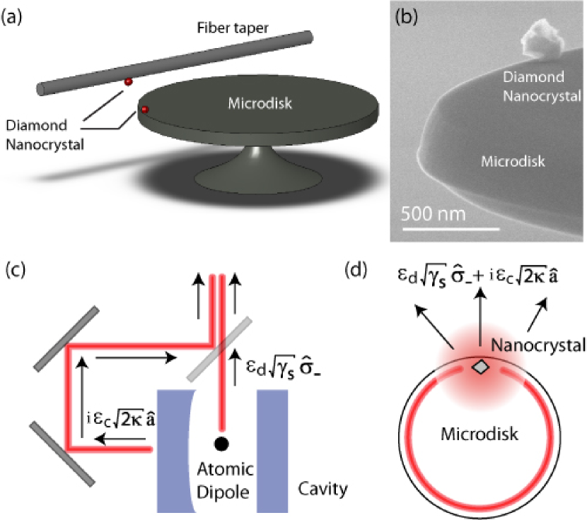
The cavity QED system studied in this Letter (Fig. 1) consists of a diamond nanocrystal containing optically active nitrogen-vacancy (NV) centers that is coupled to a dielectric microdisk cavity. Optical access to the nanocrystal-microdisk system is provided by both an optical fiber taper waveguideref:Knight and a high numerical aperture (NA=0.55) objective lens. In bulk diamond, NV centers exhibit atom-like optical properties, and are promising candidates for applications in quantum information processing, including single photon generationref:Gruber1 , coherent population trappingref:Santori2 , and optical readout and manipulation of single nuclear spinsref:Jelezko1 ; ref:Dutt1 ; ref:Childress1 . NV centers hosted in diamond nanocrystalsref:Beveratos2 are amenable to nanomanipulationref:Sandoghdar1 and integration with nanophotonic structuresref:Park1 ; ref:Wang2 . The fiber taper waveguide is a versatile tool in this regard; in addition to serving its usual role as a probe for the optical fields of the microcavity, in this work it also functions as a collection optic and a positioning tool for diamond nanocrystals. This provides several benefits, notably pre-selection of nanocrystals with optimal spectral properties from a nominally lower quality ensembleref:Shen1 , and the controlled positioning of any number of nanocrystals on photonic structures.
Light radiated from a coupled emitter (hereafter referred to as a “dipole”) and cavity system is usually described by two, distinct, source channels. The cavity radiation channel consists of the localized quasi-mode of the cavity and the radiation modes which it leaks into, whereas the dipole radiation channel consists of all other radiation modes directly coupled to the dipole emitter. In the system studied here, the radiation mode emission from the cavity mode and the dipole overlap, as illustrated for a generic Fabry-Perot cavity in Fig. 1(c), resulting in interference between the radiated field from each channel. A quantitative understanding of the interference effects can be obtained through a quantum mechanical model of the dipole-cavity system. For simplicity we consider a single mode of the microdisk which leaks into radiation modes with energy decay rate . The NV center optical transition is modeled by a single dipole transition, with excited state energy decay rate due to spontaneous emission and pure dephasing rate . The coherent-coupling rate between the dipole transition and an excitation of the microcavity mode is . The electric field radiated into the far-field by the dipole-cavity system can then be written as,
| (1) |
where is the microcavity field operator and is the polarization operator of the dipole transition. In general, the field profiles and , of radiation from the dipole and the microcavity, respectively, need not be orthogonal. The phases associated with the field operators and depend on the system and measurement geometry. In the generic example drawn in Fig. 1(c), the relative phase between the direct and indirect emission is determined by the additional path length followed by the cavity emission, and by the phase imparted by the cavity output coupling. For the nanocrystal-microdisk system (Fig. 1(d)), the path length difference can be zero.
The time evolution of the operators and can be calculated from the system density matrix equation of motion, which depends on the dipole-cavity Hamiltonian and on Lindblad operators representing the cavity and dipole decoherence processesref:Carmichael4 (see Appendix). In the “room temperature” limit, , and the detected optical spectra into a given collection optic is:
| (2) |
where is the cavity-dipole emission detuning, describes the overlap between the mode of the collection optic and that of the dipole (cavity) radiation. Note that the relative amplitude of the cavity emission scales with , the bad-cavity Purcell factor. Also note that in the room temperature limit, the effect of phonon-assisted emission on the dipole-cavity dynamics can be included as a dominant contribution to .
The microdisk cavities studied in this work are m in diameter, nm thick, and are formed by thermal oxidization of pre-patterned Si microdisksref:Borselli2 . The resulting SiO2 microdisks (refractive index ) support high- whispering-gallery-modes (WGMs) across the visible and near-infrared spectrum, with measured values as high as in the - nm wavelength band. Of particular interest are the transverse-magnetic-like (TM-like) disk modes, which are polarized primarily normal to the planar microdisk resulting in significant electric field intensity at and above the disk surface (Fig. 4(b,c)). For a wavelength of nm, near the emission wavelength of the negatively charged NV transition (NV-), the effective mode volume of the lowest radial-order () TM-like WGM (TMp=1) is calculated to be . The maximum ratio between the electric field energy density at the disk surface to that at the point of peak electric field energy density (lying within the disk) is . For the NV- transition of a nanocrystal placed at this optimal surface location, and with dipole orientation aligned normal to the disk surface, this translates into a coherent coupling rate between the TMp=1 mode and the NV- dipole of GHz. This estimate is based upon a total excited state spontaneous emission rate of MHzref:Tamarat1 . The situation, however, is complicated for the NV- transition due to electron-phonon interactions which result in signigicant coupling to several phonon sidebands. Of particular interest is coupling to the NV- zero phonon line (ZPL), which for the - fraction of spontaneous emission that is emitted into the ZPLref:Manson1 ; ref:Davies2 , yields a reduced coherent coupling rate to the TMp=1 of GHz.
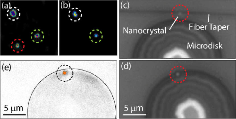
The nanopositioning scheme used to assemble individual diamond nanocrystals on the surface of the microdisks is illustrated in Fig. 1(a). A nanoscale taper formed from single mode silica fiber (Nufern 630-HP) is used both as a collection optic and as a means to pick-and-place diamond nanocrystals. The diamond nanocrystals (Diamond Innovation-NAT, 200nm median diameter) are initially sparsely dispersed on a clean silicon sample patterned with elevated mesa structures. The diamond coated silicon sample, the microdisk sample, and the optical fiber taper are mounted in an enclosed box with a dry nitrogen purge. After identifying a nanocrystal of interestref:Santori2 ; ref:Shen1 , the fiber taper is contacted on top of a nanocrystal using high resolution (50 nm) stages. The taper is then raised vertically away from the mesa surface. Due to surface interactions, which are not yet fully understood, the nanocrystal attaches to the fiber taper and is lifted from the silicon mesa surface with high yield (see Figure 2(a-b)). Transferring the nanocrystal to a microcavity follows the “pick-up” process in reverse (Fig. 2(c-d)). In order to detach the nanocrystal from the fiber taper it was found necessary to slightly move the microdisk ( m in-plane steps) when in contact with the nanocrystal so as to rub it off of the taper. Images of the microdisk after placement of the nanocrystal ( nm diameter) are shown in Figs. 1(b) and Fig. 2(e). Using this technique nanocrystals can typically be placed within a taper diameter ( nm) of the disk edge. In this case, the nanocrystal has been placed approximately nm from the disk edge. To facilitate widefield optical imaging of the nanocrystal during positioning, a relatively large particle was chosen in this instance; smaller nanocrystals can also be manipulated and positioned appropriately with the aid of confocal microscopy to identify the nanocrystal position.
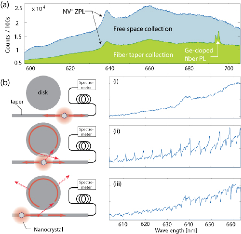
At each step in this pick-and-place process we use the fiber taper, in combination with widefield imaging optics, to study the nanocrystal emission. Figure 3(a) shows the photoluminescence (PL) spectra after the first step in which the diamond nanocrystal is attached to the fiber taper. Emission is collected both from a high-NA objective lens at normal incidence to the sample as well as through the fiber taper. Optical excitation is performed using a frequency-doubled YAG laser ( nm). The pump laser beam is sent through the collection-lens and focused down to a 1.5 m spot, with a resulting pump intensity of kW/cm2. Emission from the NV- ZPL is visible at nm, superimposed on the large phonon sideband characteristic of diamond NV centers. The measured efficiency of the fiber taper collection relative to the lens collection is . Theoretically, using smaller diameter fiber tapers (nm) and nanocrystals (nm), it should be possible to reach an absolute taper collection efficiency of ref:Klimov1 ; ref:LeKien1 .
Figure 3(b) shows measured PL spectra during the next step in the process in which the nanocrystal is brought into the near-field of the microdisk using the fiber taper. In this step the fiber taper waveguide is aligned and evanescently coupled to the microdisk with the nanocrystal positioned (i) far from the microdisk, on the nearside of the spectrometer input, (ii) nearly touching the microdisk in the taper-microdisk coupling region, and (iii) far from the microdisk, on the far side of the spectrometer input. In (i) the microdisk has no significant effect on the measured NV emission spectrum as only light directly emitted into the fiber reaches the spectrometer. In (iii) the microdisk behaves as a simple drop filter on the emission radiated into the fiber, resulting in Lorentzian dips at each of the cavity resonances. The spectrum in (ii) is more complex, with various Fano lineshapes appearing in the spectrum due to interference between the cavity and taper spontaneous emission channels (more about this below).
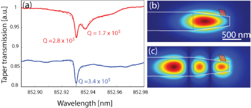
In the final step of the nanocrystal-microdisk assembly process, the nanocrystal is transferred onto the surface of the microdisk. The strong interaction between the nanocrystal and microdisk WGMs is evidenced by the effect of the nanocrystal on the WGM spectral properties. Prior to placement of the nanocrystal, the microdisk in Fig. 1(b) supports a pair of degenerate TEp=1 traveling wave WGM resonances with in the 852 nm wavelength band (blue curves of Fig. 4(a)). After placement of the nanocrystal near the disk edge, the WGM resonance splits into an asymmetric pair of standing wave resonances (red curves of Fig. 4(a)) formed from backscattering by the nanocrystalref:Weiss ; ref:Mazzei1 . The standing wave cavity modes spatially lock to the position of the sub-wavelength nanocrystal, with the anti-node (node) of the lower (higher) frequency resonance aligned with the nanocrystal. As a result, the -factor of the long wavelength resonance is degraded to due to scattering by the nanocrystal, while the -factor of the shorter wavelength resonance remains relatively close to its unperturbed value. The measured mode-splitting and scattering loss induced by the nanocrystal is in good correspondence with a perturbative analysis (see Appendix), depending upon similar cavity field properties as the dipole-cavity coherent coupling rate ref:Borselli2 ; ref:Mazzei1 .
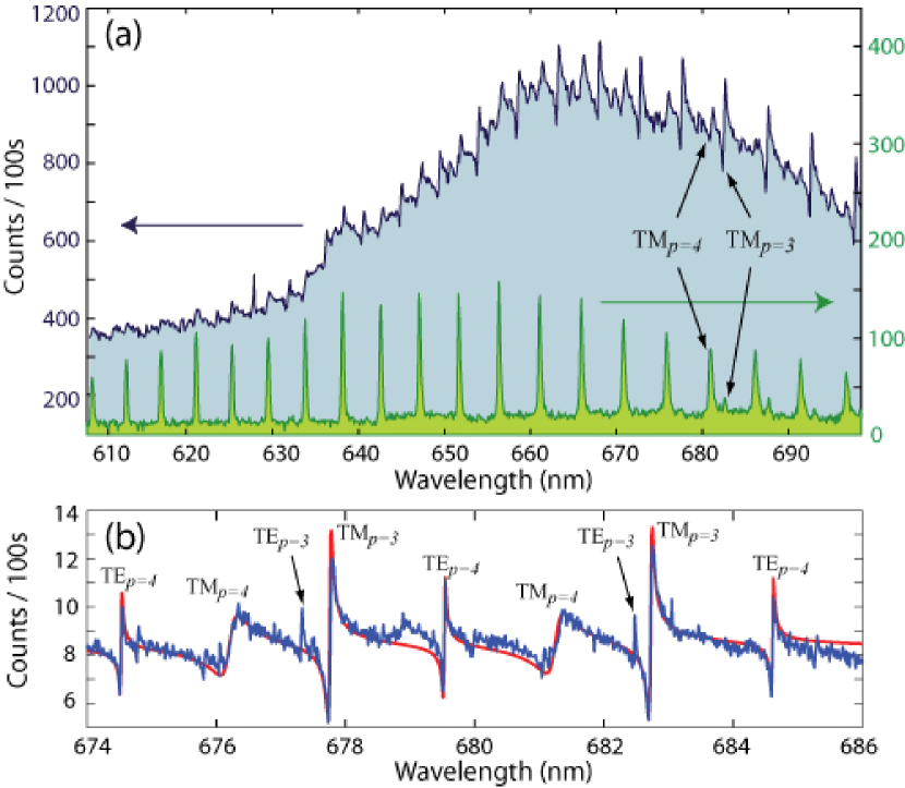
Optical excitation of the assembled nanocrystal-microcavity system shows the striking influence of the microdisk cavity, and the resulting interference between the different channels for nanocrystal emission. PL spectra collected in the far-field using the high-NA lens and the fiber taper are shown in Fig. 5. The fiber taper is evanescently coupled to the microdisk on the edge diametrically opposite from the nanocrystal, and only collects light emitted into the cavity modes of the microdisk. In both collection geometries the envelope of the collected spectrum follows the broad NV- emission characteristic of Fig. 3(b); we estimate that the nanocrystal under study here contains less than NV centers. The fiber taper PL spectrum consists primarily of regularly spaced Lorentzian peaks corresponding to the microdisk WGM resonances. The lens-collected PL, a high-resolution spectrum of which is shown in Fig. 5(b), is instead punctuated by Fano-like resonances superimposed upon the broad background spectrum of the NV- transition.
For a nanocrystal positioned on the microdisk top surface, nm from the disk edge, FEM simulations show that in the nm wavelength band the higher radial order () WGMs of the microdisk are most strongly coupled to the nanocrystal (Fig. 4(b,c)). A perturbative analysis of the scattering loss induced by the nanocrystal (see Appendix) also indicates that the values of the - radial order modes, save the TMp=4, should be limited by nanocrystal scattering. From careful comparison of the measured emission spectra with the calculated radiation-limited and nanocrystal-scattering-limited values, the various families of cavity modes in the PL from the nanocrystal can be identified, as indicated in Fig. 5. Although visible in the high-resolution lens-collected PL spectrum (Fig. 5(b)), the TEp=3,4 modes are not faithfully reproduced due to the limited resolution of the spectrometer. Note that doublet splitting is not expected for the these modes, owing to their lower-Q and large mode volume (see Appendix.) Absent from both the lens and taper collected emission spectra are the highest , radial-order modes, a result of the low spectrometer resolution which washes out narrow spectral features, and the tighter confinement of these modes inside the microdisk which weakens the coupling to the fiber taper waveguide.
To understand the measured PL spectra from the two collection geometries further, we now turn to the model described by eq. (2). For collection through the fiber taper, we observe no interference due to negligible overlap between the fiber taper mode and the radiation modes of the nanocrystal (). The resulting emission spectrum is then dominated by the second term in eq. (2) resulting in Lorentzian peaks centered at each of the microdisk cavity resonance wavelengths as seen in the measured spectrum of Fig. 5. For the far-field lens collection, when the cavity radiation is dominated by scattering from the nanocrystal, as is estimated for all but the TMp=4 modes. For a sub-wavelength nanocrystal in which the origin of the dipole emission and the scattered cavity emission nearly coincide, one can show that (see Appendix), resulting in a lens-collected power spectral density,
| (3) |
Using the above relation for , a fit to the Fano resonances of the high resolution lens-collected spectrum is performed (Fig. 5(b)). For the TMp=3 modes, which are both spectrometer-resolved and scattering-limited, the fit yields an estimate of GHz and . In the case of the spectrometer-resolved TMp=4 modes we find GHz and ; however, the reduced product for this mode family is consistent with a radiation-limited -factor for which .
Most directly, represents a ratio of the local density of states of the high- cavity modes relative to that of the radiation modes, as seen by an NV center embedded in the nanocrystal. Fitting the data gives the ratio between and , from which one can obtain by substituting the appropriate . Of particular interest is the discrete ZPL transition of the NV- state whose linewidth can approach its radiation-lifetime-limited value of MHz at cryogenic temperatures ref:Tamarat1 . Substituting MHz, GHz and for the TMp=3 resonances yields MHz. This value is roughly half that estimated from the simulated TMp=3 mode overlap with the nanocrystal ( MHz), and within a factor of 5 of the estimated maximum value for this microdisk ( MHz). Factors contributing to the smaller observed include imperfect mode-matching of the direct dipole emission and the nanocrystal-scattered cavity field, local field effects stemming from polarization of the diamond host, and the NV position(s) within the relatively large nanocrystal, for which the presence of multiple NV centers with random dipole orientations is likely to result in a lower average .
These measurements provide an initial demonstration of deterministic placement of single diamond nanocrystals on optical microcavities. Using this technique in future experiments to selectively manipulate smaller nanocrystals containing single, narrow linewidth NV centers, it should be possible to fabricate a coupled NV-cavity system with Purcell enhanced emission exceeding unity. Such a system would be an important step towards the efficient optical readout and control of the electronic and nuclear states of an NV center, and the realization of NV center based devices for quantum information processing ref:Duan1 , such as a quantum repeater. More importantly, this method may be utilized to integrate more complex diamond nanocrystal cavity QED systems, forming the basis of a chip-based quantum network.
Methods
Microdisk fabrication The microdisk optical cavities are SiO2 disks, 20 m in diameter, approximately nm thick near the disk edge, and supported by a central SiO pillar m in diameter. They were fabricated by thermally oxidizing Si microdisks in an oxygen purged furnace at a temperature of C. The template Si microdisks were fabricated from a silicon-on-insulator (SOI) wafer with a m buried-oxide-layer and a p-doped nm Si device layer of resistivity - cm. The Si microdisk processing was as follows. Electron beam lithography was used to define the microdisk pattern in a polymer electron beam resist (ZEP 520A). To improve circularity and remove surface roughness, the patterned resist was reflowed at 160C ref:Borselli2 . A SF6/C4F8 inductively coupled reactive ion etch transfers the resist pattern into the top Si layer. An HF wet etch partially removes the underlying SiO2 layer, resulting in Si microdisks supported by SiO2 posts.
Photoluminescence measurements Diamond nanocrystals containing NVs are excited optically using a frequency-doubled YAG laser ( nm). A 50X (NA = 0.55) ultralong working distance microscope objective lens focuses the excitation beam to a 1.5 m spot. Typical excitation power is W. A dichroic mirror on the backside of the objective separates NV photoluminescence from excitation power. Photoluminescence is passed through a long wavelength pass filter (cut-off nm), and then directed with a flipper mirror to either a spectrometer (resolution pm), or imaging optics and a CCD camera.
Acknowledgements
The authors thank Tom Johnson and Matt Borselli for setting up and calibrating the oxidation furnace used to oxidize the Si microdisks. This work was supported by DARPA and the Air Force Office of Scientific Research through AFOSR Contract No. FA9550-07-C-0030.
Appendix A Effective mode volume and coherent coupling rate
In this work we use the commonly defined effective mode volume of a microcavity mode in terms of its peak electric field energy density:
| (4) |
where is the refractive index profile of the cavity and is the electric field of the cavity mode. For the whispering-gallery-modes of the microdisk, the quoted effective mode volumes, unless otherwise stated, are for standing-wave resonances, which are a factor of two smaller than their traveling-wave counterparts. We use a factor to relate the peak of the electric field energy density in the cavity to the electric field energy density at a particular position (). The per photon electric field amplitude at position then relates to the effective mode volume as,
| (5) |
from which the coherent coupling rate can be estimated as . The magnitude of the dipole moment of the electronic transition, , can be determined from the spontaneous emission rate in bulk material,
| (6) |
Appendix B Mode-coupling from a sub-wavelength scatterer
The modal coupling between clockwise () and counterclockwise () traveling wave modes in a whispering-gallery-mode microcavity has been observed experimentally and explained by many other authors, including those of Refs. [ref:Weiss, ; ref:Little3, ; ref:Kippenberg, ; ref:Gorodetsky1, ; ref:Borselli2, ]. Here, we present a simple analysis of this coupling. Maxwell’s wave equation for the vector electric field in a microdisk structure is
| (7) |
where is the permeability of free space, is the dielectric function for the ideal (perfectly circular) microdisk and is the dielectric perturbation that is the source of mode coupling between the and modes. Assuming a harmonic time dependence, the modes of the ideal microdisk structure are , and are solutions of eq. (7) with . Solutions to eq. (7) with (i.e., modes of the perturbed structure) are written as a sum of the unperturbed mode basis
| (8) |
Plugging this equation into eq. (7), and utilizing mode orthogonality, we arrive at the coupled mode equations
| (9) | ||||
| (10) |
where . In deriving eq. (9) we have assumed that the mode amplitudes change slowly relative to , and that . We have also ignored small ”self term” corrections to the eigenfrequencies. Reference ref:Borselli2 presents a functional form for in situations involving small surface roughness perturbation. Under weak scattering conditions an assumption is made that only each pair of localized, degenerate and WGMs of azimuthal mode number (with dominant polarization (TE or TM) and radial mode number ) are coupled by the disk perturbation . The coupled mode equations for these traveling wave modes then read as
| (11) |
with given by the integral in cylindrical coordinates ,
| (12) |
where we have used the fact that and . For a sub-wavelength nanocrystal scatterer, the dielectric perturbation in eq. (12) can be approximated as
| (13) |
where is the free space permittivity, is the refractive index of the diamond nanocrystal () and is the physical volume of the nanocrystal. The mode-splitting in angular frequency is , and is proportional to the center frequency . The normalized mode-splitting, in terms of the traveling-wave mode effective volume (note this is twice as large as the standing-wave mode volume), can then be written as
| (14) |
where is the correction factor taking into account the reduced electric field strength at the position of the nanocrystal.
We have performed measurements of the scattering effects on the TEp=1 WGMs in the nm wavelength band of the m radius, SiO2 microdisks studied in this work. For the nm diameter nanocrystal placed on the microdisk top surface, nm from the disk edge, the ratio of the mode-splitting to the center frequency of the TEp=1 WGMs is measured to be . This corresponds well with the theoretical value predicted by eq. (14) of for a simulated traveling-wave effective mode volume and evaluated at the center of the nanocrystal ( nm above the disk surface).
Appendix C Surface-scattering from a sub-wavelength scatterer
Optical losses in whispering-gallery-mode resonators are often limited by refractive index perturbations, , on the cavity surface. These index perturbations are sourced approximately by the unperturbed field solutions to create polarization currents,
| (15) |
In analogy with microwave electronics, the polarization currents drive new electromagnetic fields which radiate into space. Optical losses due to the perturbations can be calculated from the far field solutions setup by Kuznetsov . The far field vector potential sourced by is given byKuznetsov
| (16) |
where is the wave vector in the surrounding air, and we have made the simplifying assumption that the microcavity does not significantly modify the dipole radiation from its free space radiation pattern.
For a point-like nanocrystal scatterer with perturbation given by eq. (13), and for source field corresponding to a standing-wave WGM of the microdisk, the far field Poynting vector is given by
| (17) | ||||
where is the cavity mode electric field and is the unit vector representing the polarization of the cavity mode electric field at the position of the nanocrystal scatterer. The total (cycle-averaged) power radiated, , far from the disk can be found by integrating the outward intensity over a large sphere,
| (18) | ||||
For the sphere centered about the nanocrystal scatterer, . The quality factor of a cavity is given by , where is the cycle-averaged stored energy in the cavity. The cavity energy can also be related to the effective mode volume through eq. (4). Combining all of these relations, we can rewrite eq. (18) as a scattering quality factor
| (19) |
Appendix D Finite-element-method simulations of SiO2 microdisk modes
In Table 1 and 2 we present the results of finite-element-method (FEM) simulations of the m radius, SiO2 microdisks used in this study at resonant wavelengths in the nm and nm wavelength bands, respectively. The effective index of each cavity mode is calculated from the approximate relation, , where is the azimuthal mode number of the WGM and m is the physical radius of the microdisk. The correction factors, and , correspond to the electric field energy density evaluated at the radial position of the nanocrystal ( nm from the disk edge) and vertical position at the surface of the microdisk and at the center of the nanocrystal ( nm above the disk surface), respectively. The surface-scattering-limited -factor is estimated from eq. (19) using .
| Mode | |||||||
|---|---|---|---|---|---|---|---|
| TEp=1 | 69 | 0.057 | 0.013 | 125 | 1.27 | ||
| TMp=1 | 82 | 0.061 | 0.021 | 122 | 1.24 | ||
| TEp=2 | 97 | 0.11 | 0.026 | 121 | 1.23 | ||
| TMp=2 | 106 | 0.21 | 0.069 | 118 | 1.20 | ||
| TEp=3 | 103 | 0.12 | 0.028 | 115 | 1.17 | ||
| TMp=3 | 106 | 0.24 | 0.079 | 113 | 1.15 | ||
| TEp=4 | 109 | 0.11 | 0.026 | 111 | 1.13 | ||
| TMp=4 | 111 | 0.23 | 0.077 | 109 | 1.11 |
| Mode | |||||||
|---|---|---|---|---|---|---|---|
| TEp=1 | 43 | 0.073 | 0.024 | 1.27 | 93 | ||
| TMp=1 | 51 | 0.086 | 0.040 | 1.22 | 87 |
Appendix E Nanocrystal-cavity spectrum calculation
The measured spectrum for the nanocrystal-microdisk system is given by
| (20) |
where is the component of the radiated nanocrystal-microdisk field, , collected by the microscope objective or fiber taper collection optic. is given as a function of the system variables and by eq. (1) in the manuscript text. To predict the spectrum of a spontaneous emission event, we assume that at , the dipole is prepared in its excited state and the microdisk contains no photons, and follow the techniques given in Refs. ref:Carmichael5 ; ref:Carmichael4 to calculate from and , as a function of the coupling and loss parameters of the system, , and detuning between the dipole and microdisk resonances. An outline of this method is given below.
The system Hamiltonian, which describes the dipole-cavity interaction in absence of decoherence, is given by
| (21) |
where and are the dipole transition and cavity mode frequencies, and are the dipole and cavity excitation annihilation operators, respectively, and is the coherent dipole-cavity coupling rate defined in A. Coupling between the system variables and the measured radiation field is taken into account using the quantum master equation for the system density matrix :
| (22) |
where are Lindblad operators given by:
| (23) | ||||
| (24) | ||||
| (25) |
with . () describes decay of the dipole (cavity) excitation into radiation modes, at energy decay rate (). represents decoherence of the dipole excitation, in the form of pure non-radiative dephasing at rate .
Equations of motion for the classical expectation values of and can found from the quantum master equation, using the relation :
| (26) | ||||
| (27) |
Note that in absence of an external driving field, when a dipole is initially prepared in its excited state in a cavity with zero photons, for all time . These equations of motion can be used calculate the two-time correlation functions required to determine the optical spectrum defined by eq. (20). This is accomplished using the quantum regression theorem, which, from eqs. (26) and (27), allows us to write, for ,
| (28) | ||||
| (29) | ||||
| (30) |
| (31) | ||||
Writing these equations, as well as analogous equations of motion for the special case , in the frequency domain, a closed set of algebraic equations for the various contributions to is obtained. Note that we have not assumed that the spontaneous emission process is stationary. In the room-temperature limit, , we find
| (32) | ||||
| (33) | ||||
| (34) | ||||
| (35) |
where and , and we set . From eqs. (32 - 35), eq. (20), and eq. (1) in the text, we arrive at the expression for given by eq. (2) in the text.
Appendix F Dipole-cavity radiation phase lag
Here we derive the phase difference between the radiation directly emitted from a dipole source (e.g., a diamond NV center) and the scattered radiation from a cavity resonance driven by the same dipole source. In particular we consider the situation explored in the main text in which the cavity scattering site is subwavelength and coincident with the dipole site (e.g., a diamond nanocrystal). We will show that the phase difference, , is simply due to the phase shift between driving source and local cavity field when driven on resonance. We begin with Maxwell’s equations for a microcavity defined by , a dielectric nanocrystal perturbation which couples the microcavity mode to radiation modes, and a dipole source term :
| (36) |
We have assumed that the microcavity is non magnetic, and that the vacuum dielectric and magnetic permittivities are unity.
To derive temporal equations of motion, we expand in terms of the cavity and radiation modes,
| (37) |
where are solutions to Maxwell’s equations in absence of the nanocrystal and external source,
| (38) |
and are real. It follows that are orthogonal, and we choose to normalize the fields as follows:
| (39) | ||||
| (40) | ||||
| (41) |
Note that in this mode expansion, represents a truly bound mode of the cavity: in absence of the nanocrystal or other perturbation, excitations of this mode have an infinite lifetime.
Substituting eq. (37) into eq. (36), and applying eqs. (38 - 41), for a harmonic driving term , the following coupled mode equations can be obtained:
| (42) | ||||
| (43) |
where,
| (44) |
| (45) |
In deriving eqs. (42)-(43), we have ignored “self-terms” which result in corrections to the eigenfrequencies, and have assumed that the mode amplitudes vary slowly compared to the optical frequencies. We have also assumed that the field is predominantly confined within the cavity, and that fields are predominantly excluded from the cavity. Upon integrating eq. (43) directly, and substituting the result into eq. (42), we arrive at a differential equation for . Assuming that the radiation modes form a continuum with slowly varying density of states, , and coupling coefficients, , and that coupling from the radiation modes into the cavity is negligible, a simplified equation of motion for is obtained:
| (46) |
where , and is the total energy decay rate of the cavity mode into the radiation mode continuum, due to scattering from the nanocrystal. Averaging over long times, only radiation into the mode whose frequency is resonant with the source frequency will be appreciable; the equation of motion for the mode amplitude, , is
| (47) |
where , and we have used the steady state solution for from eq. (46).
The Fano nature of radiation from the nanocrystal-cavity system can seen in the righthand side eq. (47): the first term represents emission from the source “directly” into the radiation modes, while the second term represents “indirect” emission from the source into the radiation modes via the cavity mode. Note that eq. (47) has the same form as eq. (2) in the text, the primary difference lying in the definitions of the various coupling coefficients. Here, the relative phase of the coupling coefficients is well defined by Maxwell’s equation, and can easily be determined in the case of a subwavelength scatter such as a nanocrystal.
Assuming that and , the coupling coefficients are given by,
| (48) | ||||
| (49) | ||||
| (50) |
and eq. (47), with the relative phases included explicitly, is
| (51) |
The above equation indicates that for the system of interest, when the cavity and source are on resonance, “direct” and “indirect” contributions to the radiation field are out of phase.
References
- (1) U. Fano, “Effects of Configuration Interaction on Intensities and Phase Shifts,” Phys. Rev. 124, 1866–1878 (1961).
- (2) R. W. Wood, “On the remarkable case of uneven distribution of a light in a diffractived grating spectrum,” Philos. Mag. 4, 396–402 (1902).
- (3) S. Fan, W. Suh, and J. D. Joannopoulos, “Temporal coupled-mode theory for the Fano resonance in optical resonators,” J. Opt. Soc. Am. A 20, 569–572 (2003).
- (4) C.-Y. Chao and L. J. Guo, “Biochemical sensors based on polymer microrings with sharp asymmetrical resonance,” Appl. Phys. Lett. 83, 1527–1529 (2003).
- (5) A. R. Cowan and J. F. Young, “Optical bistability involving photonic crystal microcavities and Fano line shapes,” Phys. Rev. E 68, 046 606 (2003).
- (6) J. P. Mondia, H. M. van Driel, W. Jiang, A. R. Cowan, and J. F. Young, “Enhanced second-harmonic generation from planar photonic crystals,” Opt. Lett. 28, 2500–2502 (2003).
- (7) H. Mabuchi and A. C. Doherty, “Cavity Quantum Electrodynamics: Coherence in Context,” Science 298, 1372–1377 (2002).
- (8) R. Harbers, S. Jochim, N. Moll, R. F. Mahrt, D. Erni, J. A. Hoffnagle, and W. D. Hinsberg, “Control of Fano line shapes by means of photonic crystal structures in a dye-doped polymer,” Applied Physics Letters 90, 201 105 (2007).
- (9) H. J. Carmichael, Statistical Methods in Quantum Optics 1: Master Equations and Fokker-Planck Equations (Springer, 1999), 1st edn.
- (10) J. Knight, G. Cheung, F. Jacques, and T. Birks, “Phase-matched excitation of whispering-gallery-mode resonances by a fiber taper,” Opt. Lett. 22, 1129–1131 (1997).
- (11) A. Gruber, A. Dräbenstedt, C. Tietz, L. Fleury, J. Wratchtrup, and C. v. Borczyskowski, “Scanning confocal optical microscopy and magnetic resonance on single defect centers,” Science 276, 2012–2014 (1997).
- (12) C. Santori, P. Tamarat, P. Neumann, J. Wrachtrup, D. Fattal, R. G. Beausoleil, J. Rabeau, P. Olivero, A. D. Greentree, S. Prawer, F. Jelezko, and P. Hemmer, “Coherent Population Trapping of Single Spins in Diamond under Optical Excitation,” Phys. Rev. Lett. 97, 247 401 (2006).
- (13) F. Jelezko, T. Gaebel, I. Popa, M. Domhan, A. Gruber, and J. Wrachtrup, “Observation of Coherent Oscillation of a Single Nuclear Spin and Realization of a Two-Qubit Conditional Quantum Gate,” Phys. Rev. Lett. 93, 130 501 (2004).
- (14) M. V. G. Dutt, L. Childress, L. Jiang, E. Togan, J. Maze, F. Jelezko, A. S. Zibrov, P. R. Hemmer, and M. D. Lukin, “Quantum Register Based on Individual Electronic and Nuclear Spin Qubits in Diamond,” Science 316, 1312–1316 (2007).
- (15) L. Childress, M. V. Gurudev Dutt, J. M. Taylor, A. S. Zibrov, F. Jelezko, J. Wrachtrup, P. R. Hemmer, and M. D. Lukin, “Coherent Dynamics of Coupled Electron and Nuclear Spin Qubits in Diamond,” Science 314, 281–285 (2006).
- (16) A. Beveratos, R. Brouri, T. Gacoin, J.-P. Poizat, and P. Grangier, “Nonclassical radiation from diamond nanocrystals,” Phys. Rev. A 64, 061 802 (2001).
- (17) S. Kühn and C. Hettich and C. Schmitt and J-PH. Poizat and V. Sandoghdar, “Diamond colour centres as a nanoscopic light source for scanning near field microscopy,” Journal of Microscopy 202, 2–6 (2001).
- (18) Y.-S. Park, A. Cook, and H. Wang, “Cavity QED with Diamond Nanocrystals and Silica Microspheres,” Nano Letters 6, 2075–2079 (2006).
- (19) C. F. Wang, Y.-S. Choi, J. C. Lee, E. L. Hu, J. Yang, and J. E. Butler, “Observation of whispering gallery modes in nanocrystalline diamond microdisks,” Applied Physics Letters 90, 081 110 (2007).
- (20) Y. Shen, T. M. Sweeney, and H. Wang, “Zero-phonon linewidth of single nitrogen vacancy centers in diamond nanocrystals,” Phys. Rev. B 77, 033 201 (2008).
- (21) M. Borselli, T. J. Johnson, and O. Painter, “Beyond the Rayleigh scattering limit in high-Q silicon microdisks: theory and experiment,” Opt. Expr. 13, 1515–1530 (2005).
- (22) P. Tamarat, T. Gaebel, J. R. Rabeau, M. Khan, A. D. Greentree, H. Wilson, L. C. L. Hollenberg, S. Prawer, P. Hemmer, F. Jelezko, and J. Wrachtrup, “Stark Shift Control of Single Optical Centers in Diamond,” Phys. Rev. Lett. 97, 083 002 (2006).
- (23) N. B. Manson, J. P. Harrison, and M. J. Sellars, “Nitrogen-vacancy center in diamond: Model of the electronic structure and associated dynamics,” Phys. Rev. B 74, 104 303 (2006).
- (24) G. Davies, “Vibronic spectra in diamond,” Journal of Physics C: Solid State Physics 7, 3797–3809 (1974).
- (25) V. V. Klimov and M. Ducloy, “Spontaneous emission rate of an excited atom placed near a nanofiber,” Phys. Rev. A 69, 013 812 (2004).
- (26) F. L. Kien, S. D. Gupta, V. I. Balykin, and K. Hakuta, “Spontaneous emission of a cesium atom near a nanofiber: Efficient coupling of light to guided modes,” Phys. Rev. A 72, 032 509 (2005).
- (27) D. S. Weiss, V. Sandoghdar, J. Hare, V. Lefevreseguin, J. M. Raimond, and S. Haroche, “Splitting of high-Q mie modes induceds by light backscattering in silica microspheres,” Opt. Lett. 20, 1835–1837 (1995).
- (28) A. Mazzei, S. Götzinger, L. de S. Menezes, G. Zumofen, O. Benson, and V. Sandoghdar, “Controlled Coupling of Counterpropagating Whispering-Gallery Modes by a Single Rayleigh Scatterer: A Classical Problem in a Quantum Optical Light,” Phys. Rev. Lett. 99, 173 603 (2007).
- (29) L. M. Duan and H. J. Kimble, “Scalable Photonic Quantum Computation through Cavity-Assisted Interactions,” Phys. Rev. Lett. 12, 127 902 (2004).
- (30) B. E. Little and S. T. Chu, “Estimating surface-roughness loss and output coupling in microdisk resonators,” Opt. Lett. 21, 1390–1392 (1996).
- (31) T. J. Kippenberg, S. M. Spillane, and K. J. Vahala, “Modal coupling in traveling-wave resonators,” Opt. Lett. 27, 1669–1671 (2002).
- (32) M. L. Gorodetsky, A. A. Savchenkov, and V. S. Ilchenko, “Ultimate Q of optical microsphere resonators,” Opt. Lett. 21, 453–455 (1996).
- (33) M. Kuznetsov and H. A. Haus, “Radiation Loss in Dielectric Waveguide Structures by the Volume Current Method,” IEEE J. Quan. Elec. 19, 1505–1514 (1983).
- (34) H. J. Carmichael, R. J. Brecha, M. G. Raizen, H. J. Kimble, and P. R. Rice, “Subnatural linewidth averaging for coupled atomic and cavity-mode oscillators,” Phys. Rev. A 40, 5516–5519 (1989).