Dynamics of electronic transport in a semiconductor superlattice with a shunting side layer
Abstract
We study a model describing electronic transport in a weakly-coupled semiconductor superlattice with a shunting side layer. Key parameters include the lateral size of the superlattice, the connectivity between the quantum wells of the superlattice and the shunt layer, and the conduction properties of the shunt layer. For a superlattice with small lateral extent and high quality shunt, static electric field domains are suppressed and a spatially-uniform field configuration is predicted to be stable, a result that may be useful for proposed devices such as a superlattice-based TeraHertz (THz) oscillators. As the lateral size of the superlattice increases, the uniform field configuration loses its stability to either static or dynamic field domains, regardless of shunt properties. A lower quality shunt generally leads to regular and chaotic current oscillations and complex spatio-temporal dynamics in the field profile. Bifurcations separating static and dynamic behaviors are characterized and found to be dependent on the shunt properties.
I Introduction
Theoretical work by Esaki and Tsu EsakiT70 in 1970 was the first to propose a Bloch oscillator based on a superlattice (SL) structure. In that paper, they derived current-voltage (I-V) characteristics of a SL which showed negative differential conductivity (NDC) associated with Bloch oscillationsBloch28 ; Zener34 of the miniband electrons under a DC bias. However, direct observation of Bloch oscillations is difficult due to decoherence caused by electron scattering. In other important early work, Ktitorov, Simin and Sindalovskii KtitorovS72 predicted a negative high-frequency differential conductivity and associated amplification of high frequency signals thereby suggesting an alternative means of THz oscillation. This dynamic conductivity remains negative up to the Bloch frequency and reaches a resonance minimum at a frequency closely below , suggesting that the SL may serve as an active medium for THz radiation.

However, no such devices have been realized to date more than three decades after their proposal because the NDC causes space-charge instability. Although Bloch oscillations have been observed experimentally in undoped SLs FeldmannL92 by studying optical dephasing of Wannier-Stark ladderMendezA88 excitations using degenerate four-wave mixing,YajimaT79 ; LeoS91 the gain achievable is too small to build electrically active Bloch oscillators. For high current densities, the space-charge instability causes moving charge accumulation layers (CALs) and charge depletion layers (CDLs) and thus the SL exhibits oscillations similar to the Gunn effect.Gunn63 While devices based on these oscillations may operate in the microwave range, they do not extend to the THz region.SchomburgH97
The lack of suitable THz radiation sources and detectors hampers the technological exploitation of the frequency regime spanning from 300 GHz to 10 THz. Quantum cascade laser devices have been shown to operate in the THz range for temperatures up to 164 K.WilliamsK05 On the other hand, if superlattice-based Bloch oscillators could be successfully realized they might be expected to have certain advantages relative to the quantum cascade structures.WillenbergD03 Recently, rapid progress in THz technology THz including biomedical sensing, three-dimensional imaging and chemical agent detection has attracted renewed attention to Bloch oscillators. Some structures have been proposed to stabilize the field in the SL against NDC-related instabilities. One scheme theoretically proposed by Hyart et al.HyartA08 is the dc-ac-driven SL which requires the presence of an initial THz pump. The SL is biased in the NDC region under a DC electric field, initially superposed with an AC pump electric field which stabilizes the field distribution.Kroemer Then the initial pump field can be gradually turned off when THz oscillation has been already established in the SL. Another suggestion is to stack a few short SLs, where domains are not able to form.SavvidisL04 These short SLs are separated by heavily doped material, and an increase in terahertz transmission at dc bias has been observed.
Yet another scheme is to open a shunting channel parallel to the SL, similar to a method that has been used to stabilize tunnel diode circuits.BaoW06 ; WallmarkV63 Daniel et al. DanielG05 used a distributed nonlinear circuit model to simulate the electric field domain suppression in a SL. They have shown that the shunt is able to suppress the voltage inhomogeneity above a critical bias voltage which depends on the shunt width, the SL width, and the shunt resistivity. However, the circuit model does not include aspects of the electronic tunneling transport that appear to play an important role in SL behavior. The model possesses only a global coupling since the elements are connected in series and the characteristic of each element is fixed. On the other hand, the SL model has a more complex structure that has both a global coupling due to the applied voltage constraint as well as a nearest neighbor coupling arising from the varying charge densities that dynamically change the local current density vs. field () characteristics. As a result, the nonlinear circuit model of Daniel et al. is not able to exhibit connected field domains or current self-oscillations that are observed in SL structures both theoretically and experimentally.BonillaG05
In similar work by Feil et al.,FeilT05 a side layer is grown on the cleaved edge of a lightly doped GaAs/AlGaAs SL, such that a 2D electron gas is formed at the interface between the SL and the side layer. The lightly doped SL serves two purposes: (i) to provide a modulated potential for the 2D electron gas at the interface so that under this periodic potential, the electron gas becomes a surface SL with one lateral dimension; (ii) to provide a uniform field to this surface SL since a lightly doped SL can maintain a uniform field under external bias. While the suppression of field instabilities has been reported in this type of SL, it is still not clear whether this lateral structure will be useful as a THz oscillator.
In this paper, we study an extension of a well-established model of electronic transport in weakly-coupled superlattices by adding a shunting side layer. Our treatment includes the effect of lateral electronic (i.e., horizontal) transport within each of the quantum well layers. Here, the vertical electron dynamics is associated with sequential resonant tunneling between weakly-coupled quantum well layers, rather than miniband transport or Wannier-Stark hopping as occurs for strongly-coupled SLs. Although the Bloch oscillator generally requires a strongly-coupled SL, the weakly-coupled SL has similar NDC features in I-V characteristics and similar current self-oscillations occur due to recycling of electronic fronts.WillenbergD03 ; Wacker02
In the next section, we establish a two-dimensional model for describing the current flow and dynamical electric field profile in a shunted SL. In section III, we discuss the extremely different time scales involved in this model, which are challenges to numerically solving it. In section IV, we numerically explore the effect of a high quality shunt on the dynamics of SLs as the lateral size of the SL is varied, and show that the uniform field configuration is stable, provided that the shunt and shunt connection have high enough quality and the SL lateral extent is not too great. In section V, we choose a laterally narrow SL and study the dependence of the SL dynamics on the shunt properties. The transition from a stable uniform field configuration to static field domains is found to be complex and the bifurcations involved in this transition are discussed. The Appendix presents details of the numerical methods employed.
II Laterally extended model of the superlattice with shunt layer
Weakly-coupled semiconductor superlattices have been successfully described by the sequential resonant tunneling model over the past several years.SCH01 ; Wacker02 ; BonillaG05 ; XuT07 However, previous works usually consider only the dynamics along the growth (vertical) direction of the SL and ignore the dynamics in the in-plane (lateral) direction, i.e., treat each period as an infinitely large plane with uniform charge density. More recently, Amann et al.AmannS05 developed a theoretical framework which describes both lateral and vertical electronic dynamics. Here, we extend this framework to include the effects of a shunting side layer.
The structure of the shunted SL is shown in Fig. 1. Each quantum well forms a slab that is parallel to the plane, with cross sectional dimensions and . There are such quantum wells stacked on top of each other in the direction, sandwiched between an emitter layer and a collector layer. The shunt layer is located between , with thickness . The SL period is , where and are the width of the quantum well and width of the barrier, respectively. The external voltage is applied in the direction, across the emitter and the collector.
Inside the SL, the electrons are localized within one quantum well due to the relatively thick quantum barriers. Furthermore, the electrons are assumed to be at local equilibrium and the local two-dimensional charge density at time is denoted by , where is the well index, , are the in-plane coordinates. The charge continuity equation in the SL can be written as:
| (1) |
where
| (2) |
and denotes the three dimensional vertical current in direction tunneling through each barrier (units: [A/m2]) and is the lateral two-dimensional current density (units: [A/m]). The electron charge is . The -dependence is ignored and Eq. (1) can be rewritten as:
| (3) |
The local vertical tunneling current through each barrier is described by the sequential resonant tunneling model which has been derived using different methods;Wacker02 ; BonillaG05 ; XuT07 in this paper, we have used the same form as in Refs. BonillaG05, ; XuT07, . This tunneling current depends on the electric field across the barrier through which the tunneling occurs and the electron charge densities and in the neighboring quantum wells of this barrier. Thus, the tunneling current has the functional form:
| (4) |
The tunneling current densities through the emitter and collector layers are modeled by Ohmic boundary conditions,AmannS05 that is, , and , with contact conductivity and two-dimensional doping density in each well.
The lateral dynamics is caused by the in-plane current which consists of a drift part and a diffusion part. When the -dependence is ignored, this becomes
| (5) |
where is the in-plane component of the electric field at in well , is the mobility and is the diffusion coefficient. The generalized Einstein relation CHE00 establishes the connection between and for arbitrary two-dimensional electron densities including the degenerate regime:
| (6) |
with the two-dimensional density of states , where is the electron effective mass. Here we assume that and are fixed.
Both the lateral and vertical currents depend on the electrical fields which in turn depend on the scalar potential . The potential can be solved by the Poisson equation
| (7) |
with
| (8) | |||||
| (9) |
where and are the relative and absolute permittivity, respectively. Then the field can be calculated as
| (10) |
Here we solve the Poisson equation using an approximation method assuming that the typical structures in the lateral direction vary on a length scale much longer than the mean free path of the degenerate electrons.AmannS05
The drift-diffusion dynamics of the shunting layer is similar to that of the lateral dynamics within each SL quantum well. First, we neglect -dependence in the shunt, that is, the shunt is collapsed into a single layer along the -direction. Note also that unlike the SL, which possesses an intrinsic discreteness along direction, the shunt is a continuous layer. Therefore, we make a further approximation that the shunt is divided into blocks aligned with the periods of the SL and that the charge density is locally uniform within each block. This assumption not only provides the discretization required by numerical simulation, but also matches the dynamics of the shunt with that of the SL. With these two assumptions, we can write down the continuity equation in the -th shunt block as follows:
| (11) |
where the superscript denotes the quantities in the shunt and the tilde denotes that the quantities are three-dimensional, i.e.,
| (12) |
Here, the quantity denotes the lateral current that flows between the shunt and the SL through their interface. Then we can write Eq. (11) in the form:
| (13) |
Note that the vertical current in the shunt has a very different form than the tunneling current in the SL. It follows a similar dynamics as the in-plane current in the SL quantum wells and is related to the three-dimensional charge density in the shunt:
| (14) |
Here we assume the mobility and the diffusion coefficient have the same values as in the SL.
Next, we examine the lateral current that connects the shunt and the quantum well layer within the SL:
| (15) |
In this equation, the boundary should be defined at for calculation of both the current and the potential in the shunt. Since the shunt is assumed to be uniform in direction, defining the above equation at implies that and are zero which would lead to zero boundary current. Another advantage of choosing the boundary at is that the potential in the shunt should be equal to the potential in the SL close to its boundary, i.e., , since the potential is continuous everywhere. This relation allows us to equate the potential in the shunt with that at the inner boundary of the SL. So the potential at the boundary of the solution of Eq. (7) is just the potential in the shunt. The fields required to calculate the current in Eq. (15) can be obtained by
| (16) |
The charge density and its normal gradient at the boundary are
| (17) | |||||
| (18) |
Here we also note the possible effects of energy band structure of the shunted SL and the doping density in the shunt. In the above discussion, the situation has been simplified because no band bending is included. However, variations in doping densities in the shunt and the SL can cause band bending effects at the interface. Even if the shunt is doped to have the same Fermi level as that in the SL so that little band bending might be expected, there are other issues that impact the connection quality between the shunt and the SL, for example, the presence of trap states or a thin oxide layer. To quantify the quality of the connection between the SL and the shunt, we introduce a parameter such that corresponds to a perfect connection and corresponds to no connection. We modify Eq. (15) to be
| (19) |
The relationship between specific values of parameter and microscopic models of conduction across the shunt-SL interface are discussed elsewhere.Xuu
Similarly, we introduce a separate parameter that allows us to model the effect of having different doping density and/or mobility in the shunt vs. SL quantum wells. Also recognize that the field in the shunt is almost uniform and when the conductance in the shunt is high, where is the doping density in the shunt. This leads to the following modification of Eq. (14),
| (20) |
where . Note that when the doping density in the shunt is greater than that in the quantum wells and is much less than one when the shunt is weakly conducting so that only a small fraction of the total vertical current flows through it.
It is also useful to point out that the total current,
| (21) |
is the same for each period. To show this, note that the Poisson equation can be written as
| (22) |
or
| (23) |
Substituting the above equation into Eq. (3) yields
| (24) |
Then, one integrates both sides of the preceeding equation with respect to from to . Due to the vanishing boundary conditions and , the lateral terms in the above equation integrate to zero. This yields
| (25) |
which shows that the total current is independent of the well index . Note that the current through the shunt will be the dominating contribution to the total current of a SL if the shunt is thick and well-conducting. Even a completely disconnected shunt (i.e. ) contributes a constant current of to the total current of a homogeneous SL. Since we are interested in effects arising from the interaction between the SL and the shunt, we will in the following discuss the current dynamics on the basis of the SL current defined by .
III Parameters and Time scales
The parameters that we use in the simulation are listed in Table I.
| - | (m-2) | (nm) | (nm) | (m2/Vs) | (m2/s) | (K) | - |
| 40 | 9 | 4 | 10 | 0.015 | 5 | 13.18 |
We found that there are very different time scales in this complex structure which requires an implicit method of numerical iteration. The first time scale is the dielectric relaxation time in the bulk material both in the shunt and in each quantum well in the SL. It is determined by the doping density. We know that the conductivity is proportional to the charge density
| (26) |
So the dielectric relaxation time in the shunt layer and within each quantum well is approximated as
| (27) |
which is relatively fast due to the high conductivity. This is the time it takes for a fluctuation in the charge density to be neutralized within either the shunt layer or quantum wells.
The second time scale is the one in the vertical dynamics. According to the sequential resonant tunneling model, the vertical current is to the order of (A/m2) and the positive differential conductivity is of order ( m)-1. Thus, s, a much larger time scale than . Moreover, from numerous previous works, we also know that the behavior of the electrons in the vertical direction is not simply dielectric relaxation. More complex phenomena, such as current self-oscillation, or injected dipole relocation due to switching, have much longer time scales ranging up to microseconds. The time scale sets a lower limit of the time scales for these nonlinear processes.
Another important time scale is the time that it takes to carry away or supply the electrons in the SL through the shunt. Because the vertical processes are relatively slow, if the shunt has good connection and high conductance, the electrons will move laterally, pass through the intersection between the quantum well and the shunt, and drift away through the shunt. This time scale is considerably larger than since the electrons have to move into the shunt first. Later we will see that it takes 1 ns to deplete a full CAL in a small SL. The presence of extremely different time scales means that the numerical integration is a stiff problem and this suggests the use of an implicit method. The numerical procedure is described in the Appendix.
IV Dependence of shunting dynamics on the lateral size of the Superlattice
In this section, we discuss the effects of the lateral size of the SL with a high quality shunting layer, i.e., . The shunting layer has a width such that varying does not affect the dynamics in the shunt. This is numerically confirmed even for the chaotic case that we will discuss below, where a 80 nm shunting layer has the same effect as a 8 mm one. This is because is much smaller than and the electrons entering the shunt are carried away so fast that a change in the shunt conductance does not change . We will study the SLs with a relatively high contact conductivity m. At this value of , without a shunt, the SL has a static high field domain near the emitter and a static low field domain near the collector separated by a static charge accumulation layer (CAL). Due to the high quality shunt the total current is dominated by the contribution of the current through the shunt. As discussed at the end of Section II, we will therefore consider the SL current . Also, since we are varying , we scale current to current density.
IV.1 High quality shunting layer with small
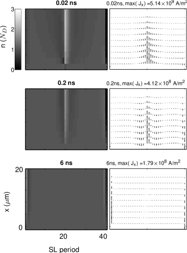
Figure 2 shows charge and current density plots for a relatively narrow SL with lateral extent m. The initial state is prepared as a charge configuration for the SL without shunt at total applied voltage V and shows a static charge accumulation layer at the 20th period. After an interval of about 1 ns, the space charge configuration is almost uniform. The in-plane current is plotted as a vector field and shows the electrons in the CAL move in the lateral direction (the opposite direction of the current) into the shunt. We can see that when the system reaches steady state, the net charge is almost neutral, i.e., , everywhere in the SL and the shunt. There are still some small lateral current flows at the first and the last period.
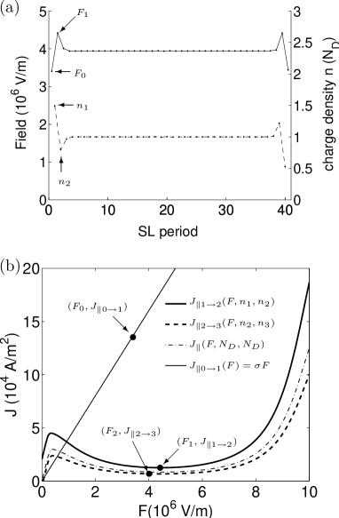
If we take a close look at the steady state, we find that there is a small CAL at the first period and a CDL nearby (Fig. 3(a)). The situation is almost inverted near the collector. To better understand this, we focus on the operation points near the emitter shown in Fig. 3(b) at m. In this case, the field is almost uniform in the SL and each period is biased in the NDC region. The field across the first barrier between the emitter and the first well will also have this same value in the absence of charge accumulation in the first well. This causes a vertical current from the emitter to the first period (thin solid line in Fig. 3(b)) which is much larger than the vertical current in the corresponding NDC region of the SL. Close to the shunt this extra current will give rise to a lateral current which will quickly reach the shunt and is carried away by the shunt. A little further away from the shunt where the lateral current is not sufficient to completely neutralize this extra current, a small CAL is formed in the first well which lowers the electric field and therefore the current across the first barrier. At the same time, the electric field in the second barrier is pushed above the uniform field, causing a very small CDL next to the CAL. Similar arguments can be applied to the collector to explain the appearance of a small CDL in the last quantum well. The overall effect is that a nearly uniform vertical electric field configuration is stabilized for these conditions.
IV.2 High quality shunting layer with large
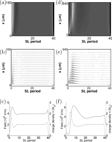
As the lateral size of the SL becomes larger, the CAL and CDL near the emitter become more prominent (cf. Fig. 4(a)-(c), m) since with increasing distance to the shunt the lateral current becomes less efficient at carrying away the excess current from the emitter to the shunt.
For wider SL (cf. Fig. 4(d)-(f), m), the field closer to the shunt is more uniform and the CAL is still attached to the emitter. However, away from the shunt, the CAL detaches from the emitter and locates itself in the first few periods and the nonuniform field region becomes larger. This behavior is due to the lateral current being insufficient to carry away the extra current from the emitter. Thus, the CAL grows bigger and tends to move toward the collector. With the center of the CAL located in different wells at different positions, the lateral gradients can be increased and a sufficient lateral current can be sustained. The field profile at m is plotted in Fig. 4(f). Field domains are forming as the field is low to the left of the CAL and high to the right of the depletion region. In this case, the upstream CAL (closer to the emitter, at the left bottom corner of Fig. 4(d)) and the downstream CAL (closer to the collector, the wider one in Fig. 4(d)) are still connected and this is a time-independent steady state.
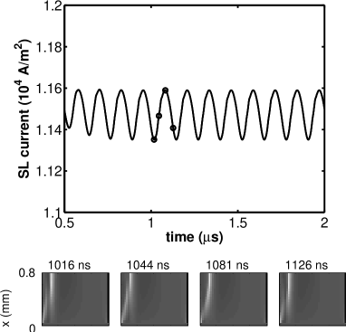
In the above case, the lateral size of the SL is just below a characteristic value for which the steady state loses stability to oscillatory behavior. Figure 5 ( m) shows the simulations of a slightly wider SL than considered above. The large downstream CAL still stays in that position. However, due to the large size of the SL, the lateral current is not able to sustain a connected stable CAL. The small upstream CAL touches and breaks off from the downstream CAL periodically. There is a small amplitude oscillation in the total current which is shown in the top panel.
For an even wider SL (Fig. 6 with 1.28 mm), the upstream and downstream CALs are mostly disconnected. The upstream CAL extends laterally into the SL and moves toward the downstream CAL, (at time 1.969 ms). For certain times during the dynamical evolution (not shown in Fig. 6), the upstream CAL breaks off from the emitter and reaches and merges with the downstream CAL. Mostly, there is a depletion region forming between the upstream and downstream CALs (2.211 ms). This depletion region grow and dies away as it merges with the upper CAL (1.969 ms). For certain times, it grows into a full CDL extending throughout the structure and, in this case, the upstream CAL also grows into a full CAL (1.755 ms). Then all three fronts move downstream. The old downstream CAL and the CDL quickly disappear and the new CAL formed by the upstream CAL replaces the old CAL and stays at its position. Although these behaviors are quite complicated, they are still periodic and during each period, the upstream and downstream CALs merge several times.
However, for an extremely wide SL (Fig. 7, mm), the behavior is apparently chaotic. The effect of the shunt is to cause a CAL attached to the emitter near the shunt. For large values of , the shunt has less effect and this CAL detaches from the emitter, tends to move downstream to the collector and thus extends toward the downstream CAL. Due to the large lateral size of the SL, the impact of the shunt layer becomes very weak on the opposite side of the SL. Thus, the downstream CAL is located very close to the 20th period where it would be in the absence of a shunting layer. The merging of the CALs described in last paragraph also appears here except that the merging events are now difficult to predict and manifestly not periodic. Figure 8 shows the behavior of a SL with mm. It should be noted that real SL samples rarely have such a large size. In this case, the unstable dynamics only occurs in the portion of the SL closest to the shunt. In the portion of the SL away from the shunt, a CAL is located at the 20th well, where the shunt has no apparent influence. Over time, the lateral extension of this CAL changes. When a large CDL collides with it at 5.696 ms, the static CAL shrinks to a small size, causing a large dip in the current trace. The presence of such charge tripole configurations AMA02 of one CDL and two CALs has already been shown to be associated with chaotic behavior in one-dimensional SL models without lateral dynamics.AMA02a
To summarize, we are able to identify three characteristic length scales in the direction. The shortest one is the decay length (of order 10 m) at which the charge density in the first quantum well increases from at the SL-shunt interface to its maximum value (cf. Fig. 4(a)-(c)). The next length scale (of order 200 m) is the range above which the vertical field configuration loses uniformity and static field domains start to form (cf. Fig. 4(d)-(f)). The longest length scale (of order 700 m) is the width of the SL above which the steady state loses stability to oscillatory behavior. This implies that lateral uniformity in the electric field distribution can be expected when is smaller than the intermediate characteristic length scale. The shortest decay length can be estimated by noting that the extra current coming from the emitter must be directed to the shunt by the negative gradient of the lateral current , i.e., . Then there is approximately a decay length , at which the quantities such as , and approach asymptotic values exponentially. Calculation shows that is of order m for the parameters used in Table I,Xuu in agreement with our numerical results.
V Dependence of dynamical behavior on the shunt properties
In the previous section, we have seen that the width of the SL determines the lateral dynamics of electronic transport and that the shunt can stabilize a nearly uniform field configuration in sufficiently narrow SLs. Now we investigate the effects of the shunt properties on a small SL with width of 20 m where the lateral field and electron density profiles are almost uniform. Since the charge density is almost uniform laterally, we modify the model such that the SL is collapsed to one point in direction. This modification significantly reduces the complexity of the simulation. We first study the effects of connectivity parameter on a SL with conductivity m chosen as in the previous section. Then we study the effects of on a SL with lower contact conductivity m, which corresponds to moving fronts and current self-oscillations in unshunted SLs,XuT07 and briefly discuss the effects of shunt conductivity parameter and width . Since is fixed, we plot the unscaled SL current .
V.1 Dynamical behavior vs. connectivity parameter for large contact conductivity
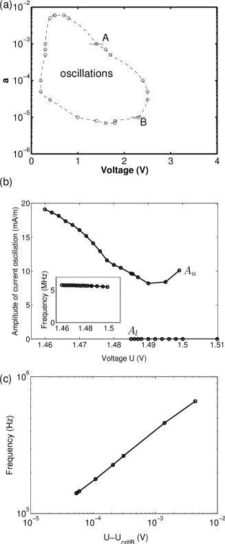
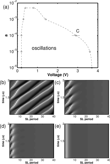
Figure 9(a) shows a bifurcation diagram using as the bifurcation parameters the connectivity parameter and the voltage for m. There is a bounded region where the system exhibits periodic or chaotic oscillations, shown as the region enclosed by dashed lines in Fig. 9(a). The value of the connectivity parameter of the oscillatory region ranges from about to . In real samples, such a weak connection between the SL and the shunt could be associated with a potential barrier formed between the SL and the shunt due to band bending or an oxide layer.
For , the charge density in the SL is almost uniform except for a small CDL near the emitter, the same situation shown in Fig. 2. With the increase of voltage, this CDL becomes more prominent and there is an CAL in the first period. However, this CAL never detaches from the emitter for any value of voltage when . This is reasonable because for , the connection is strong enough that the shunt is able to maintain the field in the SL almost uniform.
Another stable region is . In this region, a static CAL is formed in the SL and located close to the position where it is expected when there is no shunt. This is also easy to understand because the connection is so weak that the shunt has almost no influence on the SL.
Between these two values of , we have a transition region where oscillations occur for certain ranges of applied voltage. Here, the bifurcation scenarios by varying voltage are investigated for two sets of values ( and ) of the control parameters.
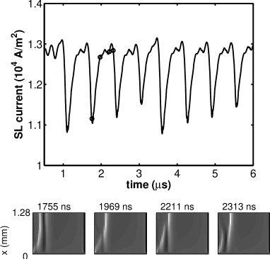
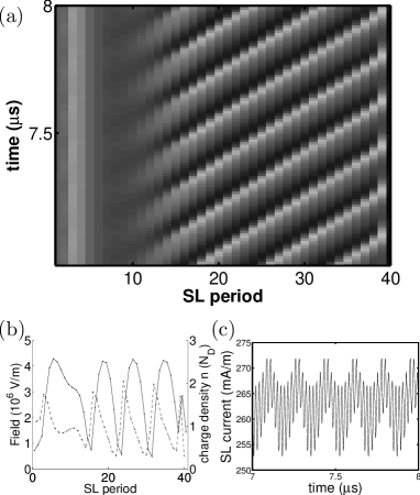
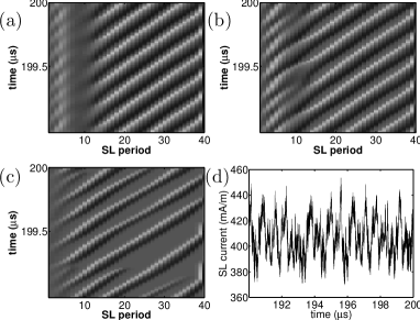
The bifurcation for point occurs at and V (Fig. 9(b), 10-12). Inside the oscillatory region (approximately V), the charge density distribution in the SL oscillates and the oscillation only involves part of the SL (cf. Fig. 10). There is a static CAL near the emitter but this is clearly detached from the emitter. The oscillation occurs in the wide region to the right of the CAL in the form of moving charge dipoles (CALs and CDLs), cf. Fig. 10(a). However, at any given time, there are three to four pairs of dipoles present. From Fig. 10(b), we can see that the charge densities have large amplitude fluctuations along the direction and the higher frequency component of the current oscillation is due to the movement of these dipoles (Fig. 10(c)). This higher frequency is nine times the lower one at which the collector receives the moving dipoles. Here we observe the coexistence of static CAL and steady moving fronts.
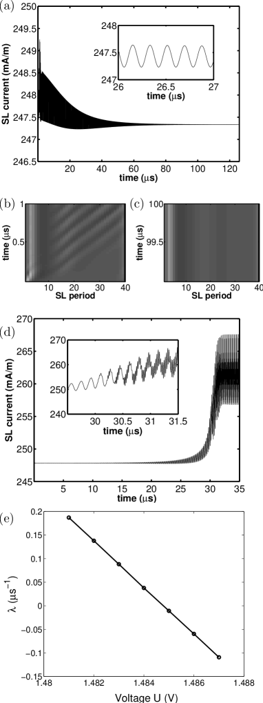
The bifurcation scenario of A is illustrated by Fig. 9(b), where the amplitude of the current oscillation is plotted versus the applied voltage. There is a bistability region between V and 1.50 V, where the system either oscillates (upper branch) or is in a steady state (lower branch).
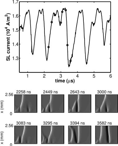
The bifurcation at point at the end of the lower branch is studied in Fig. 11. When the system starts from a uniform configuration at V, shown in Fig. 11(a), (b), (c), it first oscillates similar to the full oscillation in Fig. 10, except that the CALs and CDLs are much smaller in Fig. 11(b). The oscillation gradually decays to a steady state where there is only a single stable CAL and no charge fronts to its right, as shown in Fig. 11(c). The amplitude of the current oscillation is quite small and decays to zero. The well-to-well hopping of the small charge fronts does not have an appreciable effect on the current oscillation form as found for the mature fronts in Fig. 10(c). Instead, the shape of the current oscillation is smooth and sinusoidal and possesses a well-defined frequency. After a transient interval, the amplitude of the current oscillation decays exponentially, i.e., and the rate can be determined by fitting. It also should be mentioned that the initial state corresponding to the uniform field configuration falls into the basin of attraction of the upper oscillatory branch for V. Hence, to obtain for the lower branch, we start the system from the steady state of V. This initial state is used for all the points of the lower branch. In the case of V, shown in Fig. 11(d), the amplitude of the current oscillation increases exponentially at first and after passing a certain threshold value, quickly evolves into the large oscillations of the upper branch. The inset shows the transition region and indicates that the small charge fronts grow into mature ones. The rate can also be fitted and now it is positive. The resulting versus is plotted in Fig. 11(e), showing a linear scaling. This clearly indicates that the bifurcation at is a subcritical Hopf bifurcation. Supercritical Hopf bifurcations in different SL models have been found by Patra et al.PatraS98 and by Hizanidis et al HIZ05 at low contact conductivity with no shunt. Here we can also see that the time scales have the following relationship: .
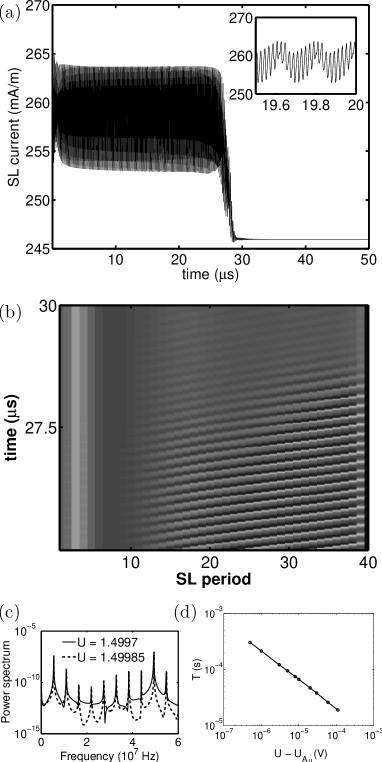
It is likely that the bifurcation scenario at in Fig. 9(b) is a saddle-node bifurcation which is probably caused by the collision of the stable limit cycle and the unstable limit cycle that arises from the subcritical Hopf bifurcation at . In Fig. 12(c), the power spectrum of the limit cycle ( V) and the power spectrum of the transient oscillation at V - which exceeds the saddle-node bifurcation value - are almost identical. This rules out a subcritical torus bifurcation. Then we start the system from a configuration corresponding to the steady oscillation at V, but for voltages just above where there are no limit cycle states, so it eventually reaches the lower branch. Figure 12(a) shows this process at V. After a short time interval of about 1 s, the oscillation amplitude enters a regime of transient oscillations and after a relatively long time , it suddenly exits this region and reaches a steady state. This process looks like a reverse process of Fig. 11(d). Figure 12(b) shows the decay of the CALs and CDLs. If we choose the critical value to be 1.499791 V, then the slope in Fig. 12(d) is -0.5. This means that , consistent with a system that undergoes a saddle-node bifurcation of limit cycles.strogatz
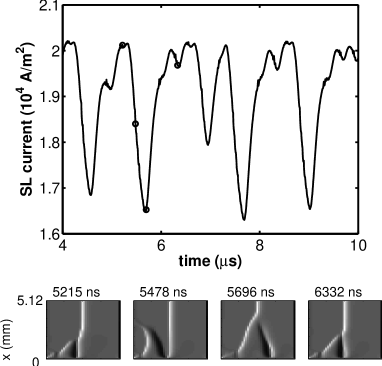
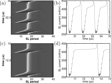
The bifurcation at point is at (Fig. 13). For V, the system oscillates. At first, there is a single CAL in the SL and a dipole is injected from the emitter. The CAL and dipole all move into the SL. The leading CDL moves about twice as fast as the two CALsAmannS05jsp and when it catches up with the original CAL, they annihilate. The CAL of the dipole continues to move forward until it reaches the position of the original CAL and stays there for a certain period of time, waiting for another round of dipole injection. Such a bifurcation of a stationary domain state has been reported before by Hizanidis et al. HizanidisB06 for a one-dimensional superlattice model without shunt at higher contact conductivity. The time needed for a dipole to be injected is called the activation time and the time needed to return from the excited state to the fixed point is called the excursion time.HizanidisB06 As the applied voltage approaches the boundary, the activation time becomes longer and longer. Taking the critical value of voltage to be 2.30441 V and plotting the frequency of oscillation versus , we find the frequency obeys the square-root law which is the characteristic scaling law for the saddle-node infinite period bifurcation or SNIPER,HizanidisB06 which is a global bifurcation of a limit cycle.
Inside the oscillatory region in the parameter space (Fig. 9(a)), we also find regimes of chaos. We still use . As the voltage decreases inside the oscillatory region, the oscillation shown in Fig. 10 involves a larger part of the SL and the CAL near the emitter becomes less and less prominent until these moving dipoles cover almost all the SL shown Fig. 14(a),(b) at V and V. Further decrease of the voltage causes the disappearance of the static CAL and the dipoles either annihilate inside the SL or reach and disappear at the collector, shown in Fig. 14(c) for V. Similar chaotic behavior has also been found in SLs without a shunt.AmannS05jsp These complicated and apparently chaotic oscillations are found at many points in the oscillatory regime of Fig. 9(a).
In the regime of the stable states between and (cf. the right hand region of Fig. 9(a)), the SL usually has a static CAL either inside the SL (for low ) or attached to the emitter (for high ) and there is a small static CDL to the right of this CAL. This means that the overall field profile is nearly uniform for larger (), but static field domains form as decreases.
V.2 Dynamical behavior for small contact conductivity
The bifurcation scenario for lower contact conductivity is simpler than for the high case. Figure 15 shows the bifurcation diagram for (m-1). This value of corresponds to current self-oscillation in the SL when there is no shunt.XuT07 The parameter space is again divided into an oscillatory regime and a stable stationary regime. The oscillatory regime starts at about the same value of as the high case, i.e., . However, this oscillatory region does not have a lower bound. This is because without the shunt the SL still exhibits oscillations.
The different behaviors at are shown in Fig. 15. As the voltage is deep inside the oscillatory region, dipoles are periodically injected into the SL and travel through the entire SL (Fig. 15(b)). As voltage increases, the distance that the dipoles travel becomes shorter and the CAL and CDL annihilate near the emitter (Fig. 15(c)). Similar behaviors have been found in a SL model without shunt.AmannS05jsp As the voltage approaches the boundary, the CDL becomes less and less prominent and the length that the CALs travel becomes even shorter. After the voltage crosses the boundary, the CALs becomes static. The bifurcation scenario is similar to point A, described in the previous section, where there is bistability between oscillatory and steady states. The bifurcation scenarios at other points on the right hand boundary of the oscillatory region appear to be similar to that at point .
V.3 Dynamical behavior vs. shunt conductivity parameter
The above discussion focuses only on varying the connectivity parameter with a shunt of high conductance. It is also possible to change other parameters of the shunt, such as the conductivity parameter in the shunt. A bifurcation diagram can be plotted for versus with fixed and nm, and it is similar to that shown in Fig. 9, with an oscillatory regime between and . Another possible control parameter is the width of the shunt. Simulation shows that only when the width of the shunt is narrower than about nm, which is unrealistically small, the SL starts to have oscillation. The oscillatory region for in Fig. 9 and 15 is almost not affected when and are above certain values so that the current between the shunt and the SL can always be supported by the shunt. In reality, and should be kept as low as possible to reduce the power dissipated in the shunt and minimize heat production.
VI Conclusions
We have theoretically studied the effect of a shunting side layer parallel to a semiconductor superlattice, and find that such a structure can have an almost uniform electric field over the entire structure even when biased in the negative differential conductivity (NDC) region. However, even for a shunt with high conductivity and strong connection to the SL, the field in the SL can be stabilized only for structures with relatively small lateral extent. As the lateral size becomes larger, the lateral current in the quantum well loses the ability to deplete the extra current coming from the emitter and the field becomes nonuniform. For a sufficiently thin SL whose lateral dynamics is uniform, the connection between the shunt and the SL and the conductivity of the shunt determines the dynamics in the SL. We have also established the bifurcation diagrams for SLs for different values of the shunt parameters and identified the presence of both local (Hopf) and global (SNIPER) bifurcations.
Although the microscopic nature of electronic transport in weakly-coupled SLs is different than for strongly-coupled SLs, the NDC property is known to produce similar dynamics in both types of structures when they are not shunted. Thus, it seems plausible that for suitable shunt connectivity and SL lateral width that a stronly-coupled SL might also be stabilized with a shunting side layer. This could enable the realization of a SL-based THz oscillator.
Acknowledgements.
This work was supported in part by NSF grant DMR-0804232, by IRCSET, and by DFG in the framework of Sfb 555.*
Appendix A Numerical method
In order to implement the implicit method, the dynamical variables, i.e. the electron densities , should be computed from the system Eqs. (3) and (13). However, are deeply buried in these equations, where the currents depend on the field that relates to by solving Poisson equation Eq. (7). So instead of solving for directly, we use the semi-implicit Euler method and numerically calculate the Jacobian matrix that is needed for this method. The procedure is as follows: after discretization of the space, the quantities of potential and charge density are placed on the grid. The fields and currents (also the charge density that is needed to calculate the currents) are placed on a staggered grid. Knowing the charge density distribution, the potential is determined by the Poisson equation using a method described in Ref. AmannS05, . After that, the currents to each grid point are calculated from the electric fields which are immediately obtained from the potential (cf. Eqs. (10) and (16)). Then the charge densities are iterated one step forward in time as
| (28) |
where is the vector whose components are the charge densities on each grid point. The first subscript denotes the SL period number and the second one is the grid point index in the direction. The vector current is the total current flow into or out of each grid point. is the new charge density configuration after time step . Since we are using the implicit method, must depend on the future charge density configuration instead of the old one. We linearize the equations:
| (29) |
where is the Jacobian matrix. Rearranging this equation yields:
| (30) |
We mentioned that the currents do not depend on the charge densities explicitly. So to calculate the Jacobian matrix, we first calculate , then slightly change the charge density at one grid point to and calculate the currents based on this charge configuration. Then one row of the Jacobian matrix is immediately obtained by .
To solve Eq. (30), we do not invert the matrix. Instead, we write it as:
| (31) |
Then we solve this set of linear equations by Gauss elimination.
References
- (1) L. Esaki and R. Tsu, IBM J. Res. Develop 14, 61 (1970).
- (2) F. Bloch, Z. Phys. 52, 555 (1928).
- (3) C. Zener, Proc. R. Soc. London, Ser A 145, 523 (1934).
- (4) S. A. Ktitorov, G. S. Simin, and V. Y. Sindalovskii, Sov. Phys. Solid State 13, 1872 (1972).
- (5) J. Feldmann, K. Leo, J. Shah, D. A. B. Miller, and J. E. Cunningham, Phys. Rev. B 46, 7252 (1992).
- (6) E. E. Mendez, F. Agulló-Rueda, and J. M. Hong, Phys. Rev. Lett. 60, 2426 (1988).
- (7) T. Yajima and Y. Taira, J. Phy. Soc. Jpn. 47, 1620 (1979).
- (8) K. Leo, J. Shah, E. O. Göbel, T. C. Damen, S. Schmitt-Rink, W. Schäfer, and K. Köhler, Phys. Rev. Lett. 66, 201 (1991).
- (9) J. B. Gunn, Solid Stat. Commun. 1, 88 (1963).
- (10) E. Schomburg, K. Hofbeck, J. Grenzer, T. Blomeier, A. A. Ignatov, K. F. Renk, D. G. Pavel’ev, Y. Koschurinov, V. Ustinov, A. Zhukov, S. Ivanov, and P. S. Kop’ev, Appl. Phys. Lett. 71, 401 (1997).
- (11) B. S. Williams, S. Kumar, Q. Hu, and J. L. Reno, Opt. Express 13, 3331 (2005).
- (12) H. Willenberg, G. H. Dohler, and J. Faist, Phys. Rev. B 67, 085315 (2003).
- (13) Phil. Trans. Roy. Soc. Lond. A., 362, (2004) special issue “THz-gap”.
- (14) T. Hyart, K. N. Alekseev, and E. V. Thuneberg, Phys. Rev. B 77, 165330 (2008).
- (15) H. Kroemer, arXiv:cond-mat/0009311 .
- (16) P. G. Savvidis, B. Kolasa, G. Lee, and S. J. Allen, Phys. Rev. Lett. 92, 196802 (2004).
- (17) M. Bao and K. L. Wang, IEEE Trans. Electron Devices 53, 2564 (2006).
- (18) J. T. Wallmark, L. Varettoni, and H. Ur, IEEE Trans. Electron Devices 10, 215 (1963).
- (19) E. Daniel, B. Gilbert, J. Scott, and S. Allen, IEEE Trans. Electron Devices 50, 2434 (2003).
- (20) L. L. Bonilla and H. T. Grahn, Rep. Prog. Phys 68, 577 (2005).
- (21) T. Feil, H.-P. Tranitz, M. Reinwald, and W. Wegscheider, Appl. Phys. Lett. 87, 212112 (2005).
- (22) A. Wacker, Phys. Rep. 357, 1 (2002).
- (23) E. Schöll, Nonlinear spatio-temporal dynamics and chaos in semiconductors (Cambridge University Press, Cambridge, 2001), Nonlinear Science Series, Vol. 10.
- (24) H. Xu and S. Teitsworth, Phys. Rev. B 76, 235302 (2007).
- (25) A. Amann and E. Schöll, Phys. Rev. B 72, 165319 (2005).
- (26) V. Cheianov, P. Rodin, and E. Schöll, Phys. Rev. B 62, 9966 (2000).
- (27) H. Xu, unpublished.
- (28) A. Amann, A. Wacker, and E. Schöll, Physica B 314, 404 (2002).
- (29) A. Amann, J. Schlesner, A. Wacker, and E. Schöll, Phys. Rev. B 65, 193313 (2002).
- (30) M. Patra, G. Schwarz, and E. Schöll, Phys. Rev. B 57, 1824 (1998).
- (31) J. Hizanidis, A. G. Balanov, A. Amann, and E. Schöll, Int. J. Bifur. Chaos 16, 1701 (2006).
- (32) S. H. Strogatz, Nonlinear Dynamics and Chaos: With Applications to Physics, Biology, Chemistry and Engineering (Westview Press, New York, 2001).
- (33) A. Amann and E. Schöll, J. Stat. Phys 119, 1069 (2005).
- (34) J. Hizanidis, A. Balanov, A. Amann, and E. Schöll, Phys. Rev. Lett. 96, 244104 (2006).