Graphene Tunneling Transit-Time Terahertz Oscillator Based on Electrically Induced p-i-n Junction
Abstract
We propose and analize a graphene tunneling transit time device based on a heterostructure with a lateral p-i-n junction electrically induced in the graphene layer by the applied gate voltages of different polarity. The depleted i-section of the graphene layer (between the gates) serves as both the tunneling injector and the transit region. Using the developed device model, we demonstrate that the ballistic transit of electrons and holes generated due to interband tunneling in the i-section results in the negative ac conductance in the terahertz frequency range, so that the device can serve as a terahertz oscillator.
Graphene is considered as a promising candidate for different future electronic and optoelectronic devices. Its most distinctive features beneficial for device applications include high electron and hole mobilities in a wide range of temperatures, the possibility of bandgap engineering (creation of the graphene-based structures with the energy gap from zero to fairly large values), formation of electrically induced lateral p-n junctions (see, for instance, 1 ; 2 ; 3 ; 4 ; 5 ).
The operation of graphene field-effect transistors (G-FETs) is accompanied by the formation of the lateral n-p-n (or p-n-p) junction under the controlling (top) gate and the pertinent energy barrier 6 ; 7 ; 8 ; 9 . The tunneling across such a n-p-n junction prevents the achievement of a low off-state current 9 . This limits possible realization of G-FETs in large scale digital electronic circuits and forces to consider the graphene structures in which the energy gap is reinstated (graphene nanoribbons and graphene bilayers with the energy gap open by the transverse electric field) 10 ; 11 ; 12 ; 13 ; 14 ; 15 ; 16 .
Unique properties of graphene already produced not only using peeling technology but also epitaxial methods as well as graphene nanoribbons and bilayers, particularly, experimental evidences of the possibility of ballistic electron and hole transport in samples with several micrometer sizes even at room temperatures (see, for instance, Refs. 17 ; 18 ) stimulate inventions of different graphene-based devices which could not be realized the past using the customary materials.
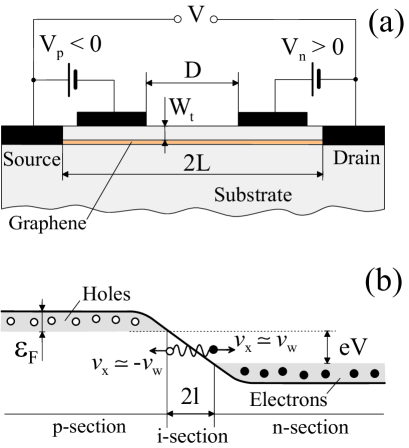
In this paper, we propose a transit-time oscillator which can operate in the terahertz (THz) range of frequencies and substantiate the operational principle of the device. The operation of the device in question is associated with the tunneling electron injection in an electrically induced reverse biased lateral p-i-n junction and the electron and hole transit-time effects in its depleted section. In the following, this device is referred to as the graphene tunneling transit-time (G-TUNNETT) terahertz oscillator. The tunneling generation through the zero energy gap and propagation of electrons and holes with their directed velocity close to the characteristic velocity cm/s of the graphene energy spectrum (), can provides significant advantages of G-TUNNETTs in comparison with the existing and discussed TUNNETTs based on the conventional semiconductor materials (see, for instance, Refs. 19 ; 20 and the references therein). Using the developed device model, we calculate the high-frequency characteristics. The device under consideration comprises a graphene layer with the source and drain contacts and the gates. The lateral p-i-n junction can be formed by two top gates biased by the dc voltages and of different polarities (, ). The G-TUNNETT structure under consideration and its band diagram (at the applied source drain-voltage , so that the lateral p-i-n junction is reverse biased) are schematically shown in Fig. 1a and Fig. 1b, respectively. It is assumed that apart from a dc component which corresponds to a recerse bias, the net source-drain voltage comprises also an ac component : , where and are the signal amplitude and frequency, respectively.
Thus, the graphene layer is partitioned into three sections: p- and n- sections adjacent to the source and drain contacts, respectively, and depleted section in the center (i-section). The depleted section of the graphene layer plays the dual role: (1) a strong electric field in the i-section provides the tunneling generation of electrons and holes and (2) this section serves as the transit region where the generated electrons and holes propagating ballistically across this region induce the current in the p- and n- sections (as well as, possibly in the contacts) and, hence, the terminal current in the source-drain circuit. Considering for definiteness the ”symmetric” device structure with ) corresponding to Fig. 1, we shall calculate its source-drain ac conductance (dynamic conductance) as a function of the structural parameters and the signal frequency and demonstrate that in certain (THz) frequency ranges.
Using the value of the interband tunneling probability 5 ; 21 , and roughly estimating the electric field in the i-section as , where is the length of the depleted i-section ( if the spacing between the top gates , were is the thickness of the layers separating the graphene layer and the gates; more strict and detailed calculations can be found in Refs. 21 ; 22 ), for the rate of the tunneling generation of electron hole pair (per unit length in the transverse direction) in the i-section in the situation under consideration one can obtain
| (1) |
Here , is the electron charge, and is the reduced Planck constant. This corresponds to the source-drain dc current
| (2) |
The ac component of the generation rate is given by
| (3) |
The tunneling probability is a fairly sharp function of the angle between the direction of the electron (hole) motion and the x-direction (from the source to the drain): , where is rather large 5 . Considering this, one can disregard some spread in the x-component of the velocity () of the injected electrons and assume that all the generated electrons and holes propagate in the x-direction with the velocity .
In the case of ballistic electron and hole transport in the i-section when the generated electrons and holes do not change the directions of their propagation, the continuity equations governing the ac components of the electrons and holes densities and can be presented as:
| (4) |
The boundary conditions are as follows: . Solving Eq. (4) with these boundary conditions, we arrive at
| (5) |
Considering this, for the net ac current , created by both the generated electrons and holes, one can obtain
| (6) |
Here, we have introduced the characteristic transit time Since the real time of the electron and hole transit across the i-section varies from to , is actually the mean transit time. If the signal frequency is smaller than the plasma oscillations in the p- and n-sections , (), these sections can be considered as just highly conducting electrodes, so that the terminal ac current is mainly induced in them. In this case, the ac component of the source-drain terminal current , i.e., the ac current induced by the propagating electrons in the external circuit connecting the source and the drain can, according to the Ramo-Shockley theorem 23 ; 24 , be presented as , where is the form-factor determined by the shape of highly conducting regions (the p-section and the drain contact) and is the i-section geometrical capacitance. The factor is associated with different contributions to the induced current of the electrons and holes at different distances from the highly conducting regions. For the bulky conducting regions , whereas for the blade-like conducting regions 25 , . For the i-section capacitance one can use the following formula: 26 , where is the dielectric constant. Considering Eqs. (3), we arrive at the following formula for the ac conductance :
| (7) |
where is the dc conductance and is the Bessel function.
The real and imaginary parts of the ac conductance are given by
| (8) |
| (9) |
where . At relatively low signal frequencies (), Eqs. (7) and (8) yield Re and Im , respectively. Thus, , i.e., is equal to the differential dc conductance . Assuming that m, m, , and V, we obtain s-1 and .
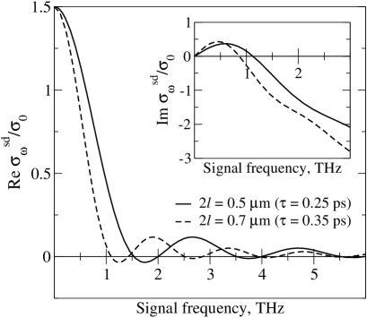
The real part of the ac conductance Re turns zero at the following signal frequencies : , , , ,… In the frequency ranges and , the real part of the ac conductance is negative. In particular, at m ( ps), THz and THz. The real part of the ac conductance reaches minima at certain frequencies , which fall into the intervals , ,… The quantity increases with increasing source-drain voltage and, consequently, dc current. A decrease in the i-section length at fixed source-drain voltage gives rise to an increase both in and in the frequencies , where exhibits manima.
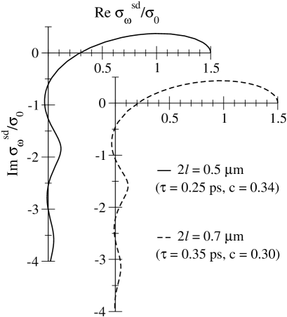
Figure 2 shows the real and imaginary parts of the ac conductance as functions of the signal frequency calculated for m and m. The real part exhibits a pronounced oscillatory behavior with the frequency ranges where it has different signs. The frequency dependence of the imaginary part corresponds to the domination of the inductive component at low frequencies (associated with the contribution of electrons and holes) and the capacitive component at elevated frequencies (due to the contribution of the geometrical capacitance). The relative value of the real part of the ac conductance at the first minima at m is fairly moderate: . However, it is markedly larger than that in some new concept THz devices 27 . Considering the above estimate of at V, one can obtain s-1. As follows from the above estimates and Fig. 2, the negativity of the real part of the ac conductance at the frequencies THz can be achieved in the G-TUNNETT structures with the i-section length only moderately smaller than one micrometer. We assumed above that the generated electrons and holes in the i-section propagate ballistically. Taking into account that the electron-electron and electron-hole scattering in this (depleted) section should be weak, the mean-free paths in graphene can be of several micrometers even at room temperatures 17 ; 18 . Our estimates show that the effect of the electron and hole space charge on the potential distribution in the i-section is weak and the pertinent plasma phenomena are insignificant.
The fundamental plasma frequency in the gated p- and n-sections, in which the spectrum of the plasma waves is a sound-like , where is the characteristic velocity, which at sufficiently high gate voltages when the electron (hole) Fermi energy in the n-section (p-section) , is given by 28 , is the spacing between the source and drain contacts, is the temperature, and is the Boltzmann constant. Since the the plasma frequency in graphene can be rather large (owing to a large ), the condition assumed above can be easily fulfilled for the signal frequencies in the THz range (as well as the condition ) by a proper choice of the device structure length and the gate voltage . Indeed, setting, for example, cm/s, m, and m, one can obtain THz.
If (or ), a G-TUNNETT coupled with the proper resonant cavity can serve as a THz oscillator. However, when (or ), i.e., when the frequency of the plasma oscillations falls into the range where Re , the hole and electron systems in the gated p- and n-sections, respectively, can play the role of the resonators. In this situation, the self-excitation of the plasma oscillations (plasma instability) can be possible if the quality factor of these oscillations , where is the frequency of hole and electron collisions with defects and acoustic phonons in the p- and n-sections, is sufficiently large 26 (see also Refs. 29 ; 30 ). It should be noted that the electron-electron and hole-hole scattering processes do not affect except as via relatively weak effects of electron and hole viscosity 31 . As a result, in sufficiently perfect graphene layers, can be small not only in the i-section but in the p- and n-sections as well. Thus, a G-TUNNETT can work as a THz source in the regime of plasma instability as well. In such a case, a G-TUNNETT should be supplied by an antenna, although the gates can also play the role of the latter.
In conclusion, we have proposed a G-TUNNETT and calculated its ac conductance as a function of the signal frequency and the structural parameter using the developed device model. We have demonstrated that the ac conductance exhibits the frequency ranges where it is negative. Due to high directed energy independent velocities of the electrons and holes generated owing to the interband tunneling, these frequency regions correspond to the THz range at relatively large length of the i-region. A G-TUNNETT can work as an active element of THz oscillators with a complemetary resonant cavity or can immediately emit THz radiation (in the plasma instability mode).
The authors are grateful to Professor T. Otsuji for stimulating discussions. The work was supported by the Japan Science and Technology Agency, CREST and by Grant-in-Aid for Scientific Research (S) from the Japan Society for Promotion of Science. The work was also partially supported by the Airforce Office of Scientific Research, U.S.A.
References
- (1) Electronic address: v-ryzhii@u-aizu.ac.jp
- (2) C. Berger, Z. Song, T. Li, X. Li, A.Y. Ogbazhi, R. Feng, Z. Dai, A. N. Marchenkov, E. H. Conrad, P. N. First, and W. A. de Heer, J. Phys. Chem. 108, 19912 (2004).
- (3) K. S. Novoselov, A. K. Geim, S. V. Morozov, D. Jiang, M. I. Katsnelson, I. V. Grigorieva, S. V. Dubonos, and A. A. Firsov, Nature 438, 197 (2005).
- (4) A. K. Geim and K. S. Novoselov, Nat. Mater. 6, 183 (2007).
- (5) J. Hass, R. Feng, T. Li, X. Li, Z. Zong, W. A. de Heer, P. N. First, E. H. Conrad, C. A. Jeffrey, and C. Berger: Appl. Phys. Lett. 89, 143106 (2006).
- (6) V. V. Cheianov and V. I. Fal’ko, Phys. Rev. B 74, 041403 (2006).
- (7) B. Huard, J. A. Sulpizio, N. Stander, K. Todd, B. Yang, and D. Goldhaber-Gordon, Phys. Rev. Lett. 98, 236803 (2007).
- (8) B. Ozyilmaz, P. Jarillo-Herrero, D. Efetov, D. A. Abanin, L. S. Levitov, and P. Kim, Phys. Rev. Lett. 99, 166804 (2007).
- (9) V. Ryzhii, M. Ryzhii, and T. Otsuji, Appl. Phys. Express, 1, 013001 (2008)
- (10) V. Ryzhii, M. Ryzhii, and T. Otsuji, Phys. Stat. Sol. (a) 205, 1527 (2008).
- (11) B. Obradovic, R. Kotlyar, F. Heinz, P. Matagne, T. Rakshit, M. D. Giles, M. A. Stettler, and D. E. Nikonov, Appl. Phys. Lett. 88, 142102 (2006).
- (12) Z. Chen, Y.-M. Lin, M. J. Rooks, and P. Avouris, Physica E 40, 228 (2007).
- (13) Y. Quyang, Y. Yoon, J. K. Fodor, J. Guo, Appl. Phys. Lett. 89, 203107 (2006).
- (14) V. Ryzhii, M. Ryzhii, A. Satou, and T. Otsuji, J. Appl. Phys. 103, 094510 (2008).
- (15) V. Ryzhii, V. Mitin, M. Ryzhii, N. Ryabova, and T. Otsuji, Appl. Phys. Express. 1, 063002 (2008).
- (16) E. McCann, Phys. Rev. B 74, 161403 (2006).
- (17) E. V. Castro, K. S. Novoselov, S. V.Morozov, N. M. R. Peres, J. M. L. dos Santos, J. Nilsson, F. Guinea, A. K. Geim, and A. H. Castro Neto, Phys. Rev. Lett. 99, 216802 (2007)
- (18) S. V. Morozov, K. S. Novoselov, M. I. Katsnelson, F. Schedin, D. C. Elias, J. A. Jaszczak, and A. K. Geim, Phys. Rev. Lett. 100, 016602 (2008).
- (19) Xu Du, I. Skachko, A. Barker, E. Y. Andrei, Nature Nanotechnol. 3, 491 (2008)
- (20) G. I. Haddad and R. J. Trew, IEEE Trans. Microwave Theory and Techniques, 50, 760 (2002).
- (21) Z. S. Gribnikov, N. Z. Vagidov, V. V. Mitin, and G. I. Haddad, J. Appl. Phys. 93, 5435 (2003).
- (22) L. M. Zhang and M. M. Fogler, Phys. Rev. Lett. 100, 116804 (2008).
- (23) M. M. Fogler, D. S. Novikov, L. I. Glazman, and B. I. Shklovskii, Phys. Rev. B 77, 075420 (2008).
- (24) W. Shockley, J. Appl. Phys. 9, 635 (1938).
- (25) S. Ramo, Proc. IRE 27, 584 (1939)
- (26) V.Ryzhii and G. Khrenov, IEEE Trans. Electron Devices 42, 166 (1995).
- (27) V. Ryzhii, A. Satou, I. Khmyrova, M. Ryzhii, T. Otsuji, V. Mitin, and M. S. Shur, J. Phys.: Conf. Ser. 38, 228 (2005).
- (28) V. N. Sokolov, K. W. Kim, V. A. Kochelap, and P. M. Muntiian, Appl. Phys. Lett. 90, 142117 (2007).
- (29) V. Ryzhii, A. Satou, and T. Otsuji, J. Appl. Phys. 101, 024509 (2007).
- (30) V. Ryzhii, A. Satou, and M. Shur, Phys. Stat. Sol.(a) 202, R113 (2005).
- (31) V. Ryzhii, A. Satou, M. Ryzhii, T. Otsuji, and M. S. Shur, J. Phys.: Condens. Matter 20, 384207 (2008)
- (32) M. Dyakonov and M. Shur, IEEE Trans. Electron Devices 43, 1640 (1996).