DFT study of Pt-induced Ge(001) reconstructions
Abstract
Pt deposited on a Ge(001) surface spontaneously forms nanowire arrays. These nanowires are thermodynamically stable and can be hundreds of atoms long. The nanowires only occur on a reconstructed Pt-Ge-surface where they fill the troughs between the dimer rows on the surface. This unique connection between the nanowires and the underlying substrate make a thorough understanding of the latter necessary for understanding the growth of the nanowires. In this paper we study possible surface reconstructions containing and of a monolayer of Pt. Comparison of calculated STM images to experimental STM images of the surface reconstruction reveal that the Pt atoms are located in the top layer, creating a structure with rows of alternating Pt-Ge and Ge-Ge dimers in a arrangement. Our results also show that Pt atoms in the second or third layer can not be responsible for the experimentally observed STM images.
pacs:
68.35.-p, 61.72.uf, 68.35.B-, 68.37.EfI Introduction
Metal/semiconductor interface interactions continue to attract interest
in both fundamental and applied research, and are of vital importance
for the semiconductor and microelectronics industry. With
miniaturization pushing into the nanoscale regime, new ways of constructing nanoscale devices are investigated. Bottom-up approaches such as atomic size reconstructions, self assembly and metal nanowires (NWs) are investigated as alternatives for the usual top-down techniques, such as etching and lithography.Barth et al. (2005)
Generally, the focus lies on metal/Si interfaces because of the importance of Si in the semiconductor industry. Of these, the Au/Si(001) interface, due to the high conductivity of Au, is one of the most well studied interfaces.
For this system, it has been shown that different types of
reconstructions appear depending on the Au coverage and the annealing
temperature.Lin et al. (1993); Kageshima et al. (2001); Shimakura et al. (1998) The
metal/Ge interface is less well studied, notwithstanding its importance in the
development of radiation detector systems and high speed electronic
devices. Recent experimental studies of the Pt/Ge(001) interface, done
at the submonolayer Pt coverage regime, have shown the formation of
self-organized Pt NW arrays after high temperature annealing.Gürlü et al. (2003); Öncel et al. (2005); Schäfer et al. (2006) It has been suggested that this reconstruction was due to a strengthened interaction of the 5
metals with the Ge surface: relativistic mass effects which contract
the shell, reducing its energy and thus increase the occupancy
at the expense of the electrons. This partially depletes the
antibonding states, strengthening the bonds.Smit et al. (2001)
The same mechanism was thought to be responsible for the one
dimensional chain structures of Au on Ge.Wang et al. (2004, 2005)
There certainly are similarities between the growth of Au and Pt chains
on Ge(001), such as the appearance of dimer vacancies before
the chains appear. Yet, there are also important differences between
the two systems. The Pt NWs only form after annealing at over 1000 K,
while the Au chains appear after deposition at 675 K and disappear into
the bulk Ge when annealed at 1000 K.Wang et al. (2005); Gürlü et al. (2003)
Moreover, while the Pt NWs have a thickness of a single atom, the Au
chains are dimer rows containing Au-Au or Au-Ge
dimers.Wang et al. (2004) The Pt NWs are thermodynamically stable and
their length is only limited by the size of the underlying terrace.
This so-called -terrace is a previously unknown Pt-Ge-surface reconstruction of which, to date, only a tentative model proposed by Gürlü
et al. exists.Gürlü et al. (2003) The unique connection
between this terrace and the NWs makes a thorough understanding of the
reconstruction desirable before one can study and understand the NW
arrays and the physical phenomena associated with
them.Vanpoucke and Brocks (2008); Stekolnikov et al. (2008)
In this work, we present a geometry for the -terrace based on the comparison of the simulated scanning tunneling microscope (STM) images
(henceforth referred to as pseudo-STM images) to experimental STM
images. The current experimental information on the
-terraces is very limited. At the moment of writing only
STM images are available. A preliminary account of this work appeared in Ref. Vanpoucke and Brocks, 2008.
The structure of this paper is as follows: In Sec. II we describe the theoretical method and introduce the notation used for the different geometries. In Sec. III we present our theoretical results starting with a comparison of the formation energies of the different geometries followed by a general review of the pseudo-STM images. We identify one particular geometry as the structure of the -terrace, which is discussed in more detail. As a last point of Sec. III, we take a look at some geometries containing Pt atoms in the second and third layer and show that these can not be responsible for the -terrace STM pictures, but they could be responsible for the indented dimer and two-dimer vacancy images seen in the STM pictures of a different Pt induced Ge(001) reconstruction, the so-called -terrace.Gürlü et al. (2003) Finally, in Sec. IV the conclusions are given.
II Theoretical method
II.1 Setup
Density functional theory (DFT) calculations are carried out using the projector augmented waves (PAW) method and the local density approximation (LDA) functional with the exchange and correlation function calculated by Ceperley and Alder (CA), as implemented in the VASP program.Blöchl (1994); Kresse and Joubert (1999); Ceperley and Alder (1980); Kresse and Hafner (1993); Kresse and Furthmüller (1996) A plane wave basis set with kinetic energy cutoff of eV is applied and the semicore shell of Ge is included in the valence shell for better accuracy. The surface is modeled by periodically repeated slabs of layers of Ge atoms. Extensive convergence tests, showed no advantage in time/accuracy for a H-passivated Ge slab over a symmetric Ge slab. Based on the advantages of the higher symmetry of the symmetric slab, we choose to use the later. The slabs are then mirrored in the -direction with reconstructions on both surfaces, in which specific Ge atoms are replaced by Pt atoms. A vacuum region of Å is used to separate the slabs along the axis. The Brillouin zone (BZ) of the surface unit cell is sampled using a Monkhorst-Pack special -point mesh.Monkhorst and Pack (1976) To optimize the geometry of the slabs the conjugate gradient method is used. The positions of the Ge atoms in the two center layers are fixed as to represent the bulk phase of the system.
II.2 Ge(001)-surface and nomenclature
To model the -terrace we first model the clean
Ge(001)-surface. Both the buckled and
reconstructions using a supercell and
the symmetric reconstruction were generated using a
supercell. After relaxation, the
and the reconstruction were found to be
and eV per dimer lower in energy than the symmetric
dimer reconstruction. A buckling angle of was found for both asymmetric reconstructions, and a
dimer length of Å for the reconstruction and of
Å for the reconstruction was calculated, all in
accordance with previous theoretical and experimental
results.Needels et al. (1987, 1988); Jenkins and Srivastava (1996); Gay and Srivastava (1999)
Based on experimental evidence, Gürlü et al. (2003); Öncel et al. (2005) we
assume that the -terrace contains monolayer (ML) of Pt. Furthermore, we assume that these Pt-atoms are located in the top layer of the Ge slab. We will show in Sec. III.4 that
Pt in the second or third layer can not be responsible for the
experimentally obtained STM images.
Formation energies and buckling angles. Pt-Ge buckling Ge-Ge buckling (meV) (degrees) (degrees) - - () (u) (u) (d) (d) (u) (u) (d) (d) (u) (u) (d) (d) () - () , - () , -
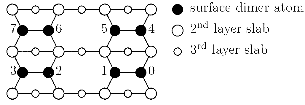
To model the -terrace, all possible non-isomorphic geometries are examined. We generate these geometries by substitution of two surface Ge atoms, of the surface reconstruction in the
supercell, by Pt atoms.
Ignoring the buckling of the Ge dimers for a moment, this leads to
seven non-isomorphic geometries. The first Pt atom replaces the Ge
surface atom in position , while the second Pt atom replaces one of
the other seven surface Ge atoms (cf. Fig. 1). We will refer to these geometries as to . If the buckling of
the Ge dimers in the reconstruction is taken into
account, some of the symmetry is lost. Let us assume for a moment that
the atoms of the dimers in Fig. 1 with an even index are
the down dimer atoms and those with an odd index are the up dimer
atoms. In what follows we will keep referring to those
positions in this manner. We now notice that in some geometries both
Pt atoms are located at an up (down)-dimer atom position and in other
cases one Pt atom is located in an up dimer atom position while the
other Pt atom is located in a down dimer atom position.fn: (a)
While for the latter all
combinations that are isomorphic stay isomorphic when
tilting is taken into account this is not the case in the former
situation. Take for example the geometry with its Pt atoms in
positions and . An isomorphic geometry in the symmetric
reconstruction is one with Pt atoms in positions and . In the
geometry, as described above, the first
geometry has both Pt atoms at down dimer atom sites, while the second
has them at up dimer atom sites. To distinguish these two different
geometries, indices and are used to indicate the up or down
location of the Pt atoms. So the first geometry is called
and the second one .fn: (b)
For geometries with one atom at an up and one at a down dimer atom site
both the and -index are used to indicate just this
(e.g. ). This results into
ten non-isomorphic geometries to start from.
To complete the picture of this system we also included
possible geometries containing ML of Pt in the top layer. Such a
surface then consists entirely of Pt-Ge dimers. Geometries
containing pure Pt and pure Ge dimers were not considered based on our
results for the -geometries.
The three possible geometries considered are a
reconstruction () with all Pt atoms at the even (or odd)
positions, a reconstruction () with the Pt atoms
at positions , , , and , and a reconstruction
() with the Pt atoms at positions , , , and
.
All these geometries were optimized using the conjugate gradient method
while keeping the positions of the Ge atoms in the two center layers
fixed.
III Theoretical results
III.1 Geometry and formation energy
III.1.1 Stability of the -geometries
The stability of the different geometries was investigated by comparison of their formation energies to the formation energy of the Ge surface reconstruction. The formation energy of a certain geometry, , can be calculated using the expression:fn: (c)
| (1) |
with the total energy of the
-geometry, the number of Pt atoms in the
system, and the bulk energy of a Ge and a Pt atom,
the total energy of the Ge surface
reconstruction and the number of surface dimers
containing Pt atoms. Negative values for indicate an increase in
stability caused by replacing a Ge atom by a Pt atom.
Table 1 clearly shows that formation energy of the -surface is much higher than that of the other structures. This is
the only structure containing a Pt-Pt dimer; all the other surface
models contain mixed Pt-Ge dimers. It shows that replacing a Ge atom in
a Pt-Ge dimer with a Pt atom will require about to eV. This
allows us to rule out the formation of Pt-Pt dimers in the
terrace. Table 1 also shows a preference for
geometries which contain Pt-Ge dimer rows with the Pt atom in the p
position. The entire set of formation energies, with the exception of ,
is spread over a relatively small energy interval of meV,
which is of the same order of magnitude as the thermal energy
corresponding to the annealing temperature. In the experiment, the germanium samples on which the Pt is deposited need to be annealed at a temperature of K ( meV) before the -terrace (and the nanowires) appear. Gürlü et al. (2003) This makes it impossible to exclude any structures based solely on energetics, with the exception of the -structure.
All formation energies are given per Pt containing dimer. This
means that the formation energy is the average energy to form a Pt-Ge dimer in the
– structures.fn: (c)
In the structures indicated with the ud-subscript the Pt-Ge
dimers are not equivalent. To make a distinction between these two types of dimers we will refer to a Pt-Ge dimer with the Pt atom in the up position as a Pt-up dimer, and similar for a Pt-down dimer. The -structure contains a Pt-up and a Pt-down dimer, while the - and -structures contain either only Pt-up or Pt-down dimers.
If we take the average of the formation energy of a Pt-up and a Pt-down dimer from the - and -structures we get meV, comparable to the formation energy of an average Pt-Ge dimer in the -structure. Comparison of the -structure with the - and -structures gives a similar result, meV for the average of the - and -structure compared to meV for the average Pt-Ge dimer. The pattern of Pt-Ge and Ge-Ge dimers in these two sets of three geometries is the same, indicating that the energy due to interactions between neighboring dimer rows is small compared to the
formation energy. In contrast, the formation energy of the Pt-Ge dimer
depends strongly on the surrounding dimers within the dimer row.
The third triplet of similarly patterned structures (, and ) shows this last point even more clearly. In this case the average of the formation energy of a Pt-Ge dimer of the - and -structure is
meV, much less than the average formation energy for a Pt-Ge
dimer in the -structure. Unlike the previous examples, the Pt-Ge
dimers of the -structure have a different surrounding along the
dimer row than those in the -structures: antiparallel instead
of parallel Pt-Ge dimers. This shows that the interaction between
neighboring dimers in a single dimer row is strong, and provides a
large contribution to the formation energy of a Pt-Ge dimer. It also
shows that rotation of a Pt-Ge dimer in the -surface cell would give
an energy gain of roughly – eV per surface unit cell.
Based on such comparisons we can make an estimate of the inter and intra dimer row energy contributions to the formation energy of a Pt-Ge dimer, . To estimate the interaction energy between neighboring dimer rows, we compare structures with different inter dimer row neighbors for the Pt-Ge dimers. Comparison of the - to the
-structures, the - to the -structure, the - to
the -structure, the - to the -structure, and - to the - and -structures, shows that this interaction energy is of the order of about – meV per Pt-Ge dimer.
A similar estimate can be made for the interaction energy
along a dimer row by comparing structures with different neighbors in a single dimer row for a Pt-Ge dimer. Comparing the - to the - and the -structures, and comparing the - to the - and -structures, gives an interaction energy in the range of – meV per Pt-Ge
dimer, about one order of magnitude larger than the inter-dimer-row
interaction energy. It also shows that the proximity of the second Pt
atom has a large influence, both for better () and for worse (),
on the formation energy. In case of the -reconstruction all Pt atoms are located at the same side of the dimer row while for the -reconstruction the Ge and Pt atoms of the dimer rows have a checkerboard pattern with the resulting surface strain deteriorating the formation energy.
Furthermore, we found that the length of the dimers was not
influenced by the different surface structures, with the sole exception of , which is the only surface structure containing a Pt-Pt dimer. The lengths
of the Ge-Ge dimers were found to be Å ( Å for ) and for the Pt-Ge dimers Å ( Å for the
Pt-Pt dimer in ). The buckling angles on the other hand do
show a dependence on the location of nearby Pt atoms. Noteworthy is the
fact that the Pt-Ge dimers show little to no buckling and the little
buckling effect they show depends on the location of the Pt atom: if
the Pt atom is located in the up position then the buckling angle is
about –, while it is less than
if the Pt atom is located in the down position.
The sign used for the buckling angles indicates wether dimers are
buckled in the same (same sign) or opposite (opposite sign) direction of the Ge surface dimers. In all cases, except and , the Pt-Ge dimers are buckled in the opposite direction of the Ge-Ge dimers thus creating a
or surface reconstruction. These
reconstructions also modify the Ge positions in the second and third
layer in a similar way as found for the Ge surface
reconstruction, which will be discussed in more detail in Sec. III.3.Needels et al. (1987); Gay and Srivastava (1999) Table 1 also shows that the Ge-Ge dimers are slightly
influenced by the Pt-Ge dimers in the same dimer row, increasing the
buckling angle to about – for Pt-Ge
dimers with the Pt atom in the up position and decreasing it to about
if the Pt atom in the Pt-Ge dimer is in the down position.
Another difference between Pt-Ge dimers with the Pt atom in the
up or down position becomes clear when the geometry of the dimers of a dimer
row containing both Pt-Ge and Ge-Ge dimers is investigated. The Pt-Ge dimer shifts
orthogonal to the dimer row. If the Pt atom is
located in the up position this shift is very small ( Å)
and almost entirely due to the Pt atom moving in the direction of the
up position. On the other hand, if the Pt atom is located in the down position, the shift is in the down direction and both the Ge and the Pt atom of the Pt-Ge dimer are shifted over a considerably larger distance of Å.
Comparison of the average -position of the dimers shows the
Pt-Ge dimers to be to Å lower than the Ge-Ge
dimers for each of the considered structures.
All the geometrical information of the Pt-Ge dimers combined with
the formation energies given in Table 1 shows
a preference for Pt atoms to be surrounded by Ge atoms which stick further out of the surface than these Pt atoms. This agrees with the preference for Ge-terminated surfaces in Pt/Ge alloys. Niranjan et al. (2007)
III.1.2 Stability of the -geometries
The stability of the -geometries is investigated the same way as for the -geometries. Equation (1) is used to calculate the formation energy per Pt containing surface dimer, making close comparison with the -geometries possible.fn: (c) In the previous paragraph we found the inter dimer row interaction to be very small, compared to the intra dimer row interaction. This allows us to compare the -geometry to the -geometries, and the and -geometries to the -geometry. The main difference between these geometries is the presence of a Ge-Ge dimer row in the -geometries. Table 1 shows the formation energies for the -geometries to be in the range expected from the comparable -geometries. As was shown in the previous paragraph, the interaction between neighboring dimer rows is relatively small for -, - and -geometries, and a larger part of the formation energy can be attributed to strain between sequential Pt-Ge dimers. For the - and -geometries the influence of the neighboring dimer rows is more important. Although the geometry of the Pt-Ge dimer in the -and -geometry is nearly indistinguishable, and thus quite different from that of the one in the -geometry, the formation energy is about the average of that of the -and the -geometry. The geometries of the Pt-Ge dimers in the - ,- and -geometries are almost identical and the angle between the antiphase Pt-Ge dimers in a dimer row is in each case about with the Pt atoms on the geometrically lower side of the dimer. Furthermore, looking at the positions of sequential dimers in a dimer row, a shift orthogonal to the dimer row is observed. This shift increases the distance between the Pt atoms with – Å in the direction orthogonal to the dimer row. It is larger than any of such shifts produced with normal Ge-Ge dimers in the dimer row, indicating the crucial role of the Pt atoms.
III.2 Electronic structure
III.2.1 General properties of the -geometries
Since there is no clear evidence based on energetics alone to put
forward a single reconstruction as the -terrace, a more
direct comparison with the STM observations is needed. This is done by
calculating the local density of states (LDOS) . Tersoff and Hamann (1985) The theoretical (integrated) LDOS is calculated as , with the Fermi energy. A surface of constant density
is then constructed according to , with C a real constant. This construction gives the height , as a function of the lateral position (), which is mapped linearly onto a gray scale. This mimics the presentation of STM images in the usual constant-current mode of operation.
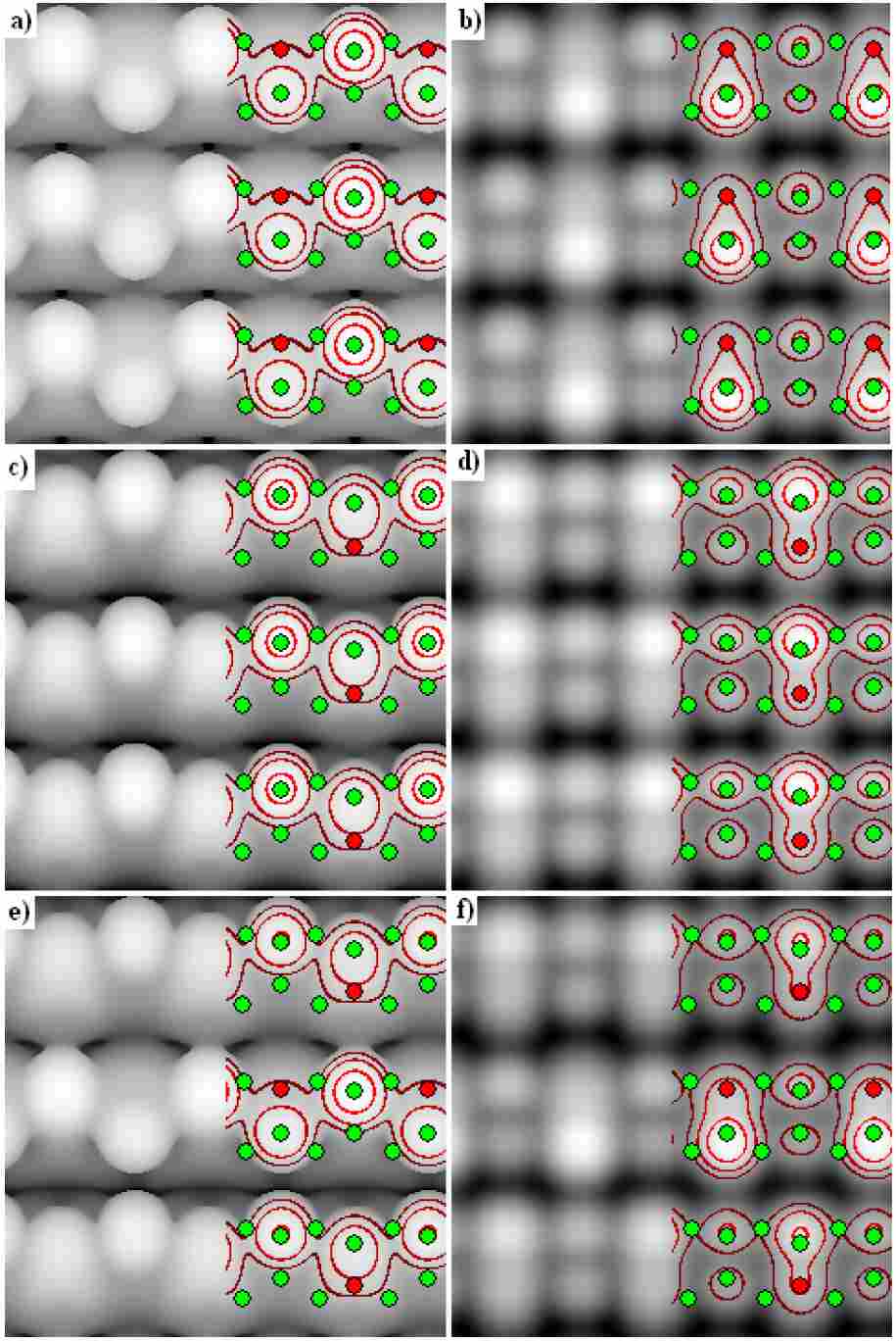
Figure 2 shows pseudo-STM images of the
-, -, and -surface for both filled and empty states. The
filled state image of the -surface shows a bright peak above
the up-atom of the Ge dimer and a slightly less bright peak above
the Ge atom of the Pt-Ge dimer. This creates a zigzag pattern of
bright spots (of two different intensities). Comparison of the
filled-state pictures of the - and -surface, shows images
for the Pt-Ge dimers that are clearly different. Where there is a
clear peak when the Pt atom was located between up-Ge atoms ()
there is a relatively evenly spread rectangular feature when the
Pt atom is located between down-Ge atoms (). This feature is
spread out over both atoms of the Pt-Ge dimer and is slightly
higher at the position of the Ge atom. The difference in height of the feature at the () positions of the dimer atoms is five times smaller than the difference in height between similar points of the feature produced by the Ge dimer. The Pt-Ge feature, in the filled-state picture, has a height equal to the average height of the Ge dimer and does not protrude as far in the
trough between the dimer rows as the Ge dimer. This gives the overall impression of ‘battlements’ (cf. all dimer rows in Fig. 2c and the upper and lower dimer row in Fig. 2e).
The -surface contains both a Pt atom between up-Ge
atoms and one between down-Ge atoms. As could be expected from the
filled-state images of the - and -surfaces the
filled-state image of the -surface shows a zigzag row and a
battlement row alternatingly. A further study of the pseudo-STM
images of the other -geometries shows these
same structures reappearing in different combinations.
A Pt atom located between up-Ge atoms causes a feature which is
about three times as steep as the feature caused by a Pt atom between
down-Ge atoms. The Pt atom is also always located at the lower end of
these features, even though sometimes the geometry shows the Pt atom to
be the higher atom of the dimer. For the
-geometries, the dimer row of the Pt-Ge dimers
shows a structure while a structure is
found in case of the -geometry. This Pt-Ge dimer row is always much
dimmer than the Ge dimer row, but it still shows nicely distinct dimer
patterns. Another careful look at the pseudo-STM structure of a Pt-Ge
dimer with the Pt atom between up-Ge atoms shows that unlike the
Ge-dimer this structure has a dim tail directed toward the Pt atom.
Although this is best visible in the empty-state pictures of Fig. 2, it is present for both filled- and
empty-state images.
The above analysis of the pseudo-STM images shows that the
filled-state images of single dimers can be used as building
blocks to reconstruct the geometry of the
-terrace (this will be shown in Sec. III.2.3).
The empty-state pseudo-STM images for a bias far above the Fermi level
show a very simple picture, with little or no dependence of the
position and size of the Pt atom features on the neighboring Ge atoms. The Ge dimer shows up as a set of two separate peaks, while the Pt-Ge dimer
is smeared out, showing a bright ball on the side of the Ge atom and a
dim wide tail on the side of the Pt atom. Though the Pt-Ge dimer images
look very similar in the empty-state pseudo-STM pictures, they are not
exactly the same. The empty-state picture of in Fig. 2 shows clearly that the Pt-Ge dimer with Pt in the
up position is slightly brighter and has a somewhat more egg-like
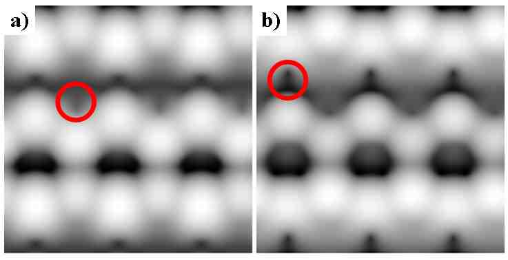
shape. Close to the Fermi level, the pseudo-STM images of filled and
empty states are nearly indistinguishable and some interesting features
appear in the pseudo-STM images. The most eye-catching feature is the
notch in the isosurface, indicated by a circle in Fig. 3a and b. It is caused by the Pt atom at that location. Though clearest for the Pt
atom between up-Ge atoms in a filled-state images and clearest for the
Pt atom between down-Ge atoms in the empty-state images, both are
present at either side of the Fermi level and were found in all
geometries. Checking contour plots of cross-sections in the
direction at the position of these notches, showed they are caused by
the gap between two lobes of the -orbitals of the Pt atom
underneath.
III.2.2 General properties of the -geometries
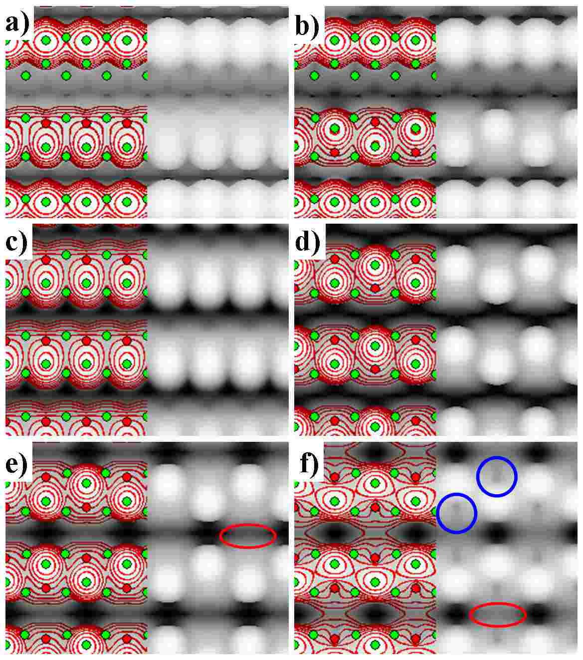
The pseudo-STM pictures of the -geometries show in general the same image for the Pt-Ge dimer rows as was seen for the corresponding Pt-Ge dimer rows in the and pictures (cf. Fig. 4). For the -geometry, the pseudo-STM pictures show dimer rows with a bright spot at the Ge atom position. This spot becomes sharper when the bias becomes smaller, both above and below the Fermi energy. The - and -geometries show nearly identical pictures (cf. Fig. 4d and e), the main difference being the phaseshift between neighboring dimer rows, which causes the appearance of a very dim (at least Å lower than the dimer peaks in the pseudo-STM pictures) bridge between the Pt atoms of neighboring dimer rows, indicated with an ellipse in Fig. 4e and f. This bridge is most clear in the empty state pictures. Again it is the Ge side of the Pt-Ge dimers which lights up very bright, causing a zigzag pattern of bright spots along each dimer row. For small biases this zigzag pattern becomes more pronounced and also the notch above the Pt atoms appears, as indicated with the circles in Fig. 4f. At a large negative bias the bright spot has a dim tail directed toward the Pt atom. All Pt-Ge dimer images for and are identical, unlike for the -geometries.
III.2.3 -structure as geometry for the -terrace
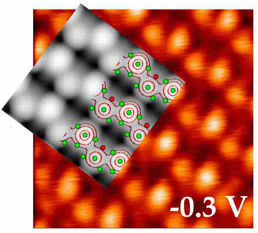
In this paragraph we will show that, although most -structures studied are energetically available, only the -geometry can be related to the experimentally observed -terrace. Figures 5 and 6 show (experimental) STM images of the -terrace at biases of V and V. The filled-state image clearly shows two types of dimers alternating in each dimer row. One of the dimer types shows up as a big bright spot on one side of the dimer row while the other dimer type shows up as a smaller somewhat dimmer spot on the other side of the dimer row, with a dim tail extending to the opposite side of the dimer row. These are the only two types of dimers appearing in the image. Comparing this to the results of the pseudo-STM images seen in the previous paragraph, the first type of dimer is the Ge-Ge dimer while the second type of dimer presents all the typical features of the Pt-Ge dimer with the Pt atom located between up-Ge atoms. This allows us to exclude all -geometries containing Pt at a down location, leaving only the -, -, and -geometry. Taking the relative ordering of the features of neighboring dimer rows into account, the geometry which represents the -terrace can only be the -geometry. Filled- and empty-state pseudo-STM images of the -geometry are displayed on top of the experimental pictures in Fig. 5 and 6.
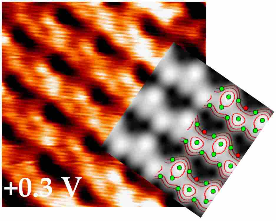
The empty-state pseudo-STM image (Fig. 6) shows some
very specific features of this geometry. There are triangular
holes where the Pt atom is located and the Ge atoms of the top layer
also create a triangular feature dominated by the zigzag structure of
the up-Ge atoms and the Ge atoms in the Pt-Ge dimers. Comparison of the
empty-state images in Fig. 6 reveals the existence
of these features in both images, further strengthening our belief that
the -geometry is the geometry of the -terrace. Another look
at Table 1 also confirms this geometry to be more
stable than the Ge surface reconstruction. Furthermore,
for the -geometries, the Pt atoms are also
distributed in the most homogeneous way.
The pseudo-STM images show only for the -geometry this level of agreement with the experimental STM images, allowing the -structure to be presented as the geometry of the experimentally observed -terrace.
Figure 8b shows the band structure of the
-geometry along the high symmetry lines
-J-K-J′--K of the surface BZ (cf. Fig. 7).
Figure 8a shows the band structure of the Ge(001)
c() reconstruction along the same lines for comparison. In
general, the two band structures show similar behavior. Perpendicular
to the dimer row direction, along the J-K and J′-
line, the bands show little dispersion. Along the J′-
line, a few of these bands cross the Fermi level. The main difference
between the two band structures is located along the -J and
K-J′ lines. For the -structure we find bands with a
strong dispersion opposite to what is seen for the Ge(001) surface. These bands are indicated with the ellipses in Fig. 8b.
Furthermore, these bands also cross the Fermi level in the second half
of the -J line and in the first half of the K-J′ line, resulting in the metallic behavior observed
for the -terrace. Gürlü (2004) Taking a closer look at
these specific bands near the crossing of the Fermi level, we find that
their character contains three main components. The largest component
has a Pt-like character. The other two (smaller) components have a
Ge-like character: more specifically, the second layer Ge atoms bound
to the Pt atoms in the top layer and the Ge up-atom of the Ge surface dimer that is located in between the Pt atoms. The orbital character of the Pt contribution is mainly
and , making it highly planar. The Ge
contribution depends on the Ge atoms involved. The orbital character of
the contribution of second layer Ge atoms is mainly , while the
top layer Ge atoms bound to the Pt atom contribute mainly a
orbital character, indicating the presence of a -bond with energy
close to the Fermi level for the Pt-Ge dimer. Interestingly, the Ge
up-atoms of the Ge dimers in between Pt atoms along the dimer row have a significant contribution to most of the bands we are interested in. The orbital character in this case is mostly and . The presence of bands
close to (and crossing) the Fermi level connected to an orbital
character directed along the dimer row direction, indicates the
possible presence of surface conduction channels along this direction.
These bands could be the source of the confined states observed in
Ref. Öncel et al., 2005 and van Houselt et al., 2006.
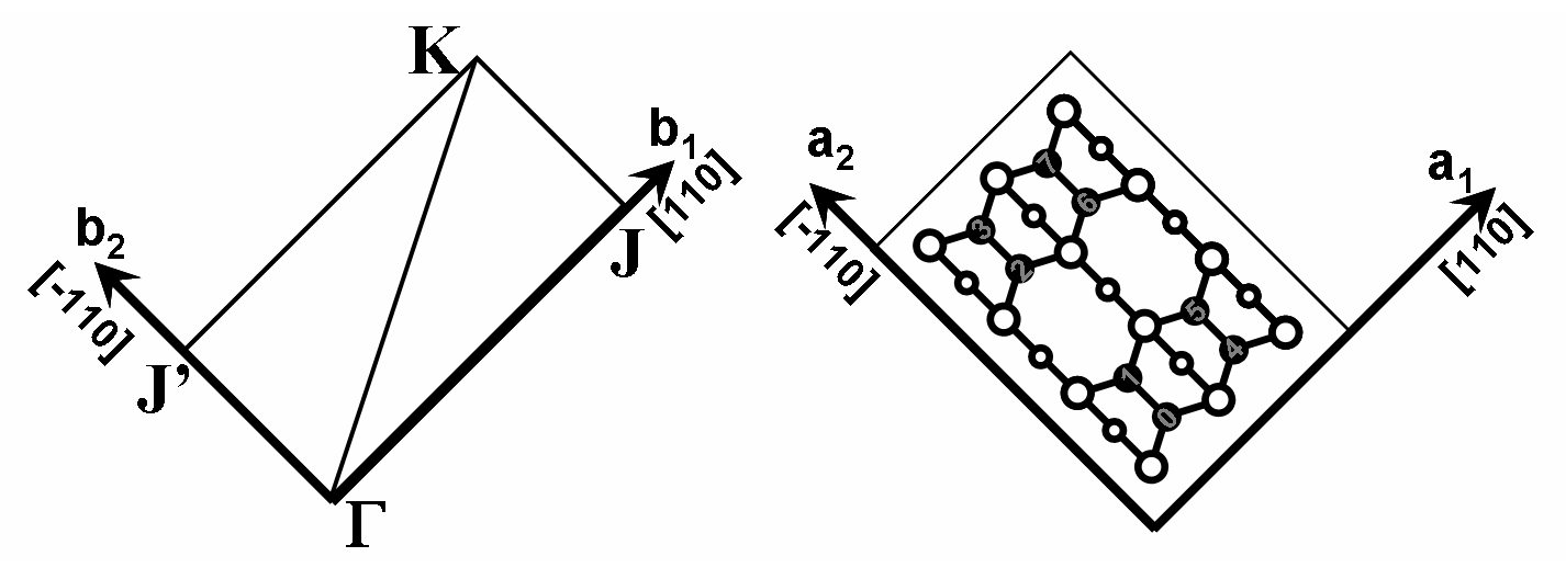
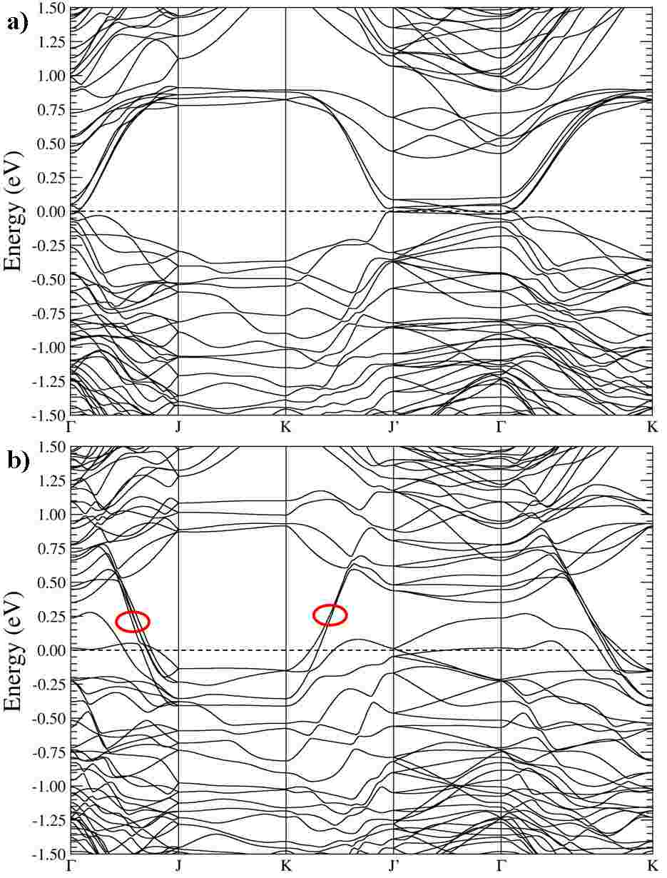
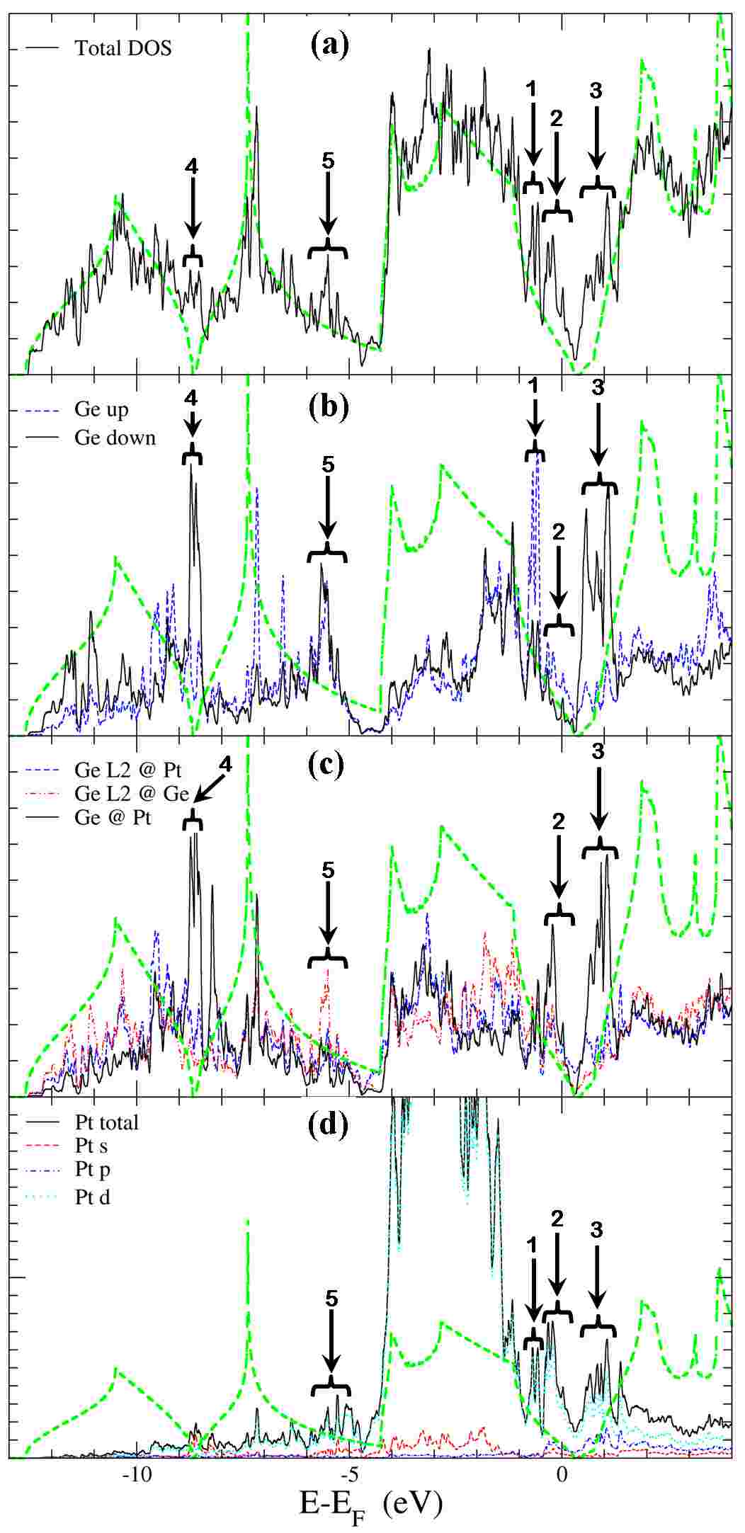
Figure 9 shows the density of states (DOS) of the -geometry and the LDOS of the surface atoms.fn: (d)
The total DOS roughly follows the DOS observed for bulk Ge, as could be
expected. The main difference is found in the band gap (BG) region. Here, three
distinct peaks can be observed, indicated by the labels , , and in Fig. 9. The two outer peaks ( and ) are also observed
for a reconstructed Ge(001) surface, where they are linked to the
dangling bonds of the Ge surface dimer atoms. Since half the surface
dimers of the -geometry are Ge dimers, it is not surprising to observe
these states. Figure 9b
shows the LDOS of the up and down atoms of the Ge surface dimers.
Comparison to the Ge(001) c and b()
reconstruction, shows the peak due to the Ge-down atom () to be quite
broad, with a width comparable to what is found for the b()
reconstruction. This broadening probably originates from the small
tilt-angle of the Pt-Ge dimers. This makes the angle between subsequent dimers in a quasi-dimer row (QDR) smaller, making it more comparable to the zero angle of the b() reconstruction. The Ge-up atom, shows two peaks in the BG ( and in Fig. 9b). The strong peak, labeled is also found for the Ge-up atom of the Ge(001) c and b() reconstructions. The weaker second peak has a non-zero value for the DOS at the Fermi level and is one of the contributions to peak in the total DOS.
The LDOS image of the Ge atoms bound directly to the Pt atom
shows something interesting (cf. Fig. 9c). The Ge atom of the Pt-Ge dimer also has two peaks in the BG region, contributing to peaks and in the total DOS. A sharp peak around the same value as seen
for the Ge down atom at the conduction band (CB) side (), and a second
peak near the valence band (VB) side of the BG region (). This second peak is located just at the Fermi level. Between these two peaks the LDOS goes to zero, just above the Fermi level.
The second layer Ge atoms (indicated with L in Fig. 9) show roughly the same structure, both have a small contribution to the conducting peak of the total DOS. However, in the
BG region it are only the second layer Ge atoms bound to the Pt atoms of the
top layer that have non-zero values over the entire BG region (cf. blue dashed curve in Fig. 9c). Second layer Ge atoms bound to the Ge atoms of the top layer have a LDOS which goes to zero. The LDOS for the Pt atoms, presented in Fig. 9d, shows the presence of Pt states at and around the Fermi level, with peaks at the same locations as found for the Ge atoms bound to these Pt atoms. For the Ge atoms, it are mainly states contributing to these peaks near the Fermi level, showing clearly the presence of a hybridization of Ge with Pt
states. Together with the Ge up-atoms and Pt atoms, the Ge atoms bound to the
Pt atoms form a corridor of ‘metallic’ atoms along the edge of the QDR, giving rise to the metallic peak of the total DOS, in agreement with the experimental observations.Gürlü (2004)
The additional peaks, and , in the total DOS are related to the surface Ge atoms, and are also observed for the Ge(001) c and b() reconstructions.
III.2.4 Experimental existence of other -geometries
Although the comparison between experimental and pseudo-STM images in
Fig. 5 and 6 shows clearly that
the clean -terrace has a -geometry, the formation energies
given in Table 1 indicate that also other
geometries should be observed experimentally. In particular the structure has a slightly lower energy. The latter structure leads to STM images that are completely different to what is observed experimentally, as do other non structures. Our calculations therefore indicate that the formation of such structures is kinetically hindered. Investigation of
experimental STM images has shown the existence of (small) regions
where dimer rows contain a mix of different (non ) geometries.
These geometries were mostly found near defects in the normal
-terrace, such as dimer vacancies and the endpoints of a
NW. Because these geometries seem related to defects, we will not
go into the details of their geometry and focus solely on the -geometry.
III.3 The -geometry
Bond lengths and dimer tilt angle. A B1 B2 C1 C2 C3 C4 d1 d2 d3 t1 t2 t3 t4 Ge b 19.42 2.450 2.512 2.426 2.475 2.449 2.543 2.475 0.815 0.775 0.099 3.818 0 0 0 Ge c 19.60 2.511 2.506 2.430 2.463 2.481 2.481 2.462 0.842 0.749 0.007 3.817 0.283 0.335 0.332 Ge-dimer 20.82 2.462 2.552 2.433 2.479 2.435 2.492 2.469 0.875 0.731 0.027 3.764 0.153 0.049 0.003 Pt-dimer 2.354 2.378 2.521 2.479 2.435 2.492 2.469 0.174 1.358 0.027 3.764 0.153 0.049 0.003
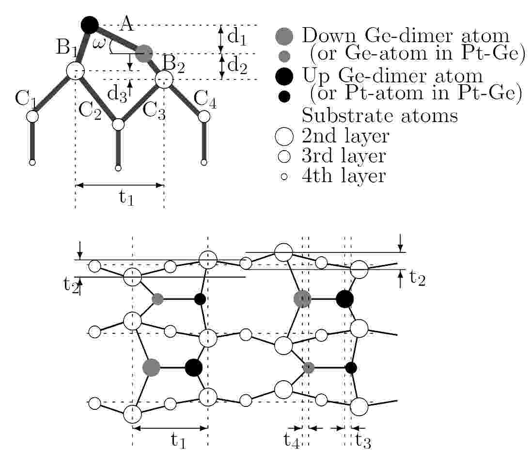
Bottom: Top view schematic representation of the -reconstruction.
To characterize the geometry of the structure, it is compared to the geometry of the Ge(001) and reconstructions. This shows a slight shift of the second and third layer Ge atoms of the structure in the surface plane with regard to the Ge equilibrium positions. In what follows we will show that this deformation of the geometry can be understood as a combination of three geometric modifications, each linked to a symmetry breaking of the top layer structure.
In the second layer of the geometry, two inequivalent sites are present: i) a Ge atom between a top layer Ge up atom and a Pt atom, and ii) a Ge atom between a top layer Ge down atom and a Ge atom of a Pt-Ge dimer. The Ge atom at the latter site is displaced toward the neighboring Ge atom of the Pt-Ge dimer, while the Ge atom at the former site is displaced toward the neighboring Ge up atom (cf. Fig. 10). In comparison to the Ge reconstruction, in the surface plane these atoms appear as twisted around the in-plane position of the third layer Ge atom in between them. For this reason, such a modification of the geometry, i.e. the twisting of the tetrahedral structure, is known as twisting.Gay and Srivastava (1999)
The Ge surface reconstruction, for which a diagrammatic representation can be found in figure of Ref. Gay and Srivastava, 1999, is a simple Ge surface reconstruction which only shows the twisting modification with regard to the reconstruction. Twisting is believed to be a strain release mechanism, where strain (orthogonal to the surface) due to different surface dimer buckling is (partially) compensated by an in-plane modification of the second layer geometry, indicated with t2 in Fig. 10. This means that the twisting parameter t2 is related to the relative buckling angle of sequential surface dimers in a dimer row. Assuming a linear relation as first order approximation one finds , where is the buckling angle shown in Table 2 for each of the dimers involved. Because the relative
angle between sequential dimers can be used as a measure for the twisting, it becomes possible to estimate the twisting for similar surfaces via the ratio of their relative buckling angle
| (2) |
where rec and rec refer to each of the two reconstructions being compared.
Unlike the twisting observed for Ge surface reconstructions with differently buckled surface dimers, the twisting found in the geometry is asymmetric. From Fig. 10 follows that t2 can be considered to consist of two parts; the component along the dimer row direction of the bond C2 and the component along the dimer row direction of the bond C3. The ratio of the contributions of C2 and C3 to t2 is for the Ge and Ge reconstructions, while it is for the reconstruction. This means that, in comparison to the Ge reconstruction, the second layer Ge atom between the Pt atom and the Ge up atom is pulled slightly back toward the Pt atom in the surface plane.
Using Eq. (2) to calculate the ratio of the twisting of the reconstruction to the Ge reconstruction making use of the values for t2 presented in Table 2 we find a value of for . However, making use of the relative buckling angle we find a value of for . Unlike the Ge reconstruction, there are different kinds of surface dimers on the surface. To include this inhomogeneity of the surface dimers in Eq. (2), we add weight factors to the angle contributions. We found the mass percentages of the dimers to be good weight factors. This leads to a twisting ratio for the to the Ge structure:
with Mx the atomic mass of a single (average) atom of type x, and the angle shown in Table 2 for the specific dimer y. Using Eq. (III.3) a value of is found for the ratio R, in agreement with the value obtained for the ratio of the t2 parameters. Also for other structures, equations equivalent to Eq. (III.3) give an improvement of the estimated ratios of t2 over the ratios obtained through Eq. (2). E.g. for the structure compared to the Ge structure, the ratio of the twisting parameters t2 is . Using the relative buckling angles in Eq. (2) one finds a value of , which is much to small. However, using the weighted buckling angles, as in Eq. (III.3), one finds a value of , in good agreement with the ratio of the parameters t2.
This shows t2 to be a useful parameter for comparison of the asymmetry induced strain in these systems. As a result, the difference of the twisting parameter, t2, between the Ge and -reconstruction can be attributed to the introduced Pt atoms. On the one hand by leveling out the Pt-Ge dimer, i.e. the term, and on the other hand through the weight factor.
In conclusion, twisting is the result of the relative buckling angle of sequential dimers in a dimer row which is influenced strongly by the Pt atoms present in the structure.
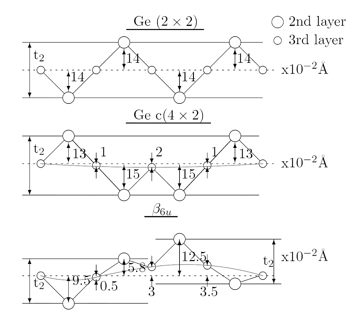
Figure 11 gives diagrams of the top view of a row of second and third layer Ge atoms in geometries with
increasing complexity. The horizontal dashed lines give an arbitrary
zero-line with regard to which all amplitudes are given. The Ge
()-reconstruction shows the simple image of twisting
of the tetrahedral arrangement, discussed above. The image of the Ge reconstruction presents, in addition to twisting, a bending of the entire second and third layer structure, indicated with the gray curve in Fig. 11. It shows a slight displacement of of the third layer Ge atoms in the plane along the dimer row direction. This is due to the asymmetry between the C1, C4 and the C2, C3 bonds as a result of the opposite buckling of dimers in adjacent dimer rows.
In the structure, just like the Ge reconstruction, the surface dimers in adjacent dimer rows show an opposite buckling which results in a bending, as shown with the gray curve in the bottom picture of Fig. 11. Furthermore, the presence of Pt atoms in the top layer dimers seems to increase the
amplitude of the bending by a factor of two and the extrema of the
bending curve move from the third layer atoms between the dimer rows
to the third layer atoms underneath the dimer rows.
The presence of two different dimer types in the structure complicates this image even further, as can be seen in the bottom picture of Fig. 11. On top of the previous two distortions a shift of the twisting t2 between adjacent dimer rows is present. Shift is the displacement of the horizontal lines defining the twisting parameter t2 between neighboring dimer rows (cf. bottom pictures of Fig. 10 and Fig. 11), in other words; it is the shift along the dimer row direction of the twisting parameter t2 its bounding box between adjacent dimer rows. This shift is a consequence of the induced asymmetry in the components along the dimer row direction of the C2 and C3 bonds contributing to t2, which in turn is due to the asymmetry of having different dimer types in a dimer row, as well as in adjacent dimer rows.
In case of the structure, the shift is directed toward the Pt-Ge dimer, away from the Ge-Ge dimer (cf. Fig. 10, bottom picture). This makes shift, which is due to different dimer types in one system, the third surface modification present in the geometry. It shrinks the surface cell, formed by the first and second layer atoms, containing the Pt-Ge dimer in favor of the Ge-Ge dimer surface cell. Table 2 also shows a decrease of the parameter t1, reducing the size of the Pt-Ge dimer surface cell even further and partially compensating the expansion of the Ge-Ge dimer surface cell.
The bond length of the Ge-dimer in the reconstruction is only
slightly longer than it was in the -reconstruction but still significantly
shorter than it is in the -reconstruction. The
accompanying change in buckling angle accounts for this slight
elongation. Also, the back bonds of the Ge atoms of all dimers are
longer than their counterparts in the asymmetric Ge surface
reconstructions. This while the height of these back bonds for the
Ge-Ge dimers is similar to the one found for the
-reconstruction. t3 and t4, shown in Fig. 10, give the in-plane displacement along the surface dimer bond direction between sequential dimers in a single dimer row, i.e. the alignment of the surface atoms along the dimer rows. Although they are not zero, they are at least one order of magnitude smaller than the values
obtained for the -reconstruction, and unlike the -reconstruction there is an asymmetry between the two displacements. his results from the difference in length of Pt-Ge and Ge-Ge bonds.
The Cn-bonds between the second and third layer Ge atoms have lost all symmetry, this is due to the two types of surface dimers present in the structure. This is unlike the reconstructions studied by Gay et al. Gay and Srivastava (1999) where only one type of surface dimer is present in each system, and as a consequence the Cn bonds show much symmetry.
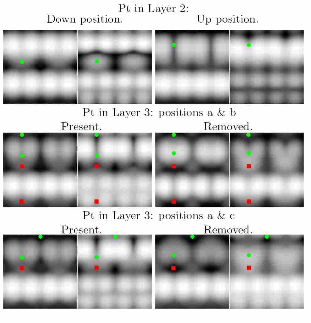
III.4 Other geometries
Though the previous section shows clearly that the -terrace has
a -geometry, it is still interesting to have a look at some
geometries containing Pt atoms in the second or third layer of the
system. Previous calculations and experimental observations have
shown that Pt atoms can also be found in subsurface
positions. Gürlü et al. (2004) Before the transformation to the
-terrace, there is what Gürlü et al. call an
-terrace. This type of terrace is characterized by a
large number of dimer vacancy defects. Also, in this initial stage of Pt growth on Ge(001) there are
still a number of features which are not entirely understood,
such as ‘indented dimers’.
Figure 12 shows the positions where Ge atoms
were substituted with Pt atoms in the second and third layer of the
system. The final geometries were obtained the same way as the
-geometries, i.e. substitution of Ge atoms by Pt atoms
in a Ge(001) b()-reconstructed slab and relaxation of the
geometry using the conjugate gradient method keeping the positions of
the two center layers fixed.
III.4.1 Pt in the second layer
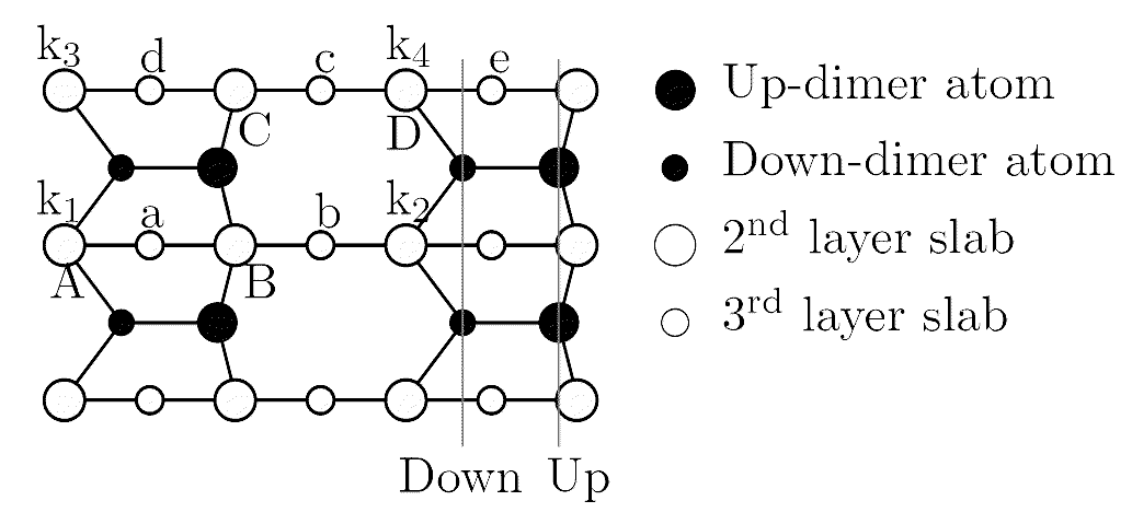
When Ge atoms in the second layer are substituted with Pt atoms, there are two possible inequivalent sites to consider. One under the down Ge atoms and one under the up Ge atoms of the surface dimers. Table 3 shows the formation energy per Pt atom for these two locations differs only meV and Pt favors the position under the up Ge dimer atoms. Table 3 also shows that the introduction of a second Pt atom in the second layer improves the stability of the system considerably, increasing the formation energy by and meV per Pt atom. This difference from what would be expected from the single Pt substitution results, shows there is a positive correlation between the Pt atoms in the second layer. Furthermore, comparison of Table 1 and Table 3 shows the formation energies per surface unit are roughly in the same range as the formation energies per surface unit of the studied - and -geometries, making these structures energetically also viable candidates for the -terraces. Pseudo-STM images on the other hand clearly show this is not the case.
Formation energy. Layer Pt position(s) (meV) A (down) 24 B (up) 40 A & D (down) 4 B & C (up) 163 a (row) 1115 (k1) a (row) 155 b (trough) 68 a & b 630 (k1& k2) a & b 467 a & c 467 (k1) a & c 66 a & d 616 (k1& k3) a & d 32 a & e 1141 (k1& k4) a & e 346
The top part of Fig. 13 shows the influence of the
substitution of a single Ge atom by a single Pt atom in the second
layer of the system. In both cases the images of the two Ge dimers on
top of the Pt atom merge into one image, with the
location of the overlap on the side where the Pt atom is located.
For a Pt atom located at the down side this fusing is only
seen for small bias voltages, for large bias the images are almost
indistinguishable from the normal Ge dimer images. Also, the
brightness of the dimers is roughly the same as for the Ge dimers
on a normal Ge(001) surface.
In case the Pt atom is located at the up side of the dimer row,
the position where the two images of the Ge dimers merge moves from
being on top of the Pt atom, for large negative biases, to being on top
of the Ge atom in between two Pt atoms, for small negative biases and
all positive biases. Also, in this case there is a clear difference in
brightness between the normal Ge dimers and the dimers on top of a Pt
atom. For negative biases, the normal Ge dimers are most bright while
for positive biases, the modified dimers are brighter. The brightest
part of the modified dimers extends over the entire dimer for small
biases, while for large positive (and negative) bias the brightest part
of the image is at the side of the up Ge atoms. This gives the
impression of a dimer located at one side of the dimer row, and
directed along this dimer row. This is only an impression because these
structures are formed by the bending, toward and away from the Pt atom,
of the Ge orbitals. When all Ge atoms at the up side in the second
layer under a dimer row are substituted by Pt atoms, the images of the
above Ge dimers do not merge anymore. Their image only lengthens and
becomes a long oval shape which is dimmer than the normal Ge dimer at
negative bias and brighter than the normal Ge dimer at positive bias.
This elongated shape persists at positive bias such that there is a
clear difference between this image and the image of a normal Ge dimer,
for which the single dimer image is replaced by two spots, one for each
Ge atom.
III.4.2 Pt in the third layer
Substitution in the third layer can also be done at two inequivalent
sites. The first is under the dimer row and the second is in the
trough, between dimer rows. Table 3 shows a
clear preference for Pt to be positioned under a dimer row, while a Pt
atom in the trough position is less favorable than the original
b()-reconstruction. This again shows the preference of Pt to
be surrounded by Ge atoms. This is understandable since the
Pt-Ge bond is energetically favorable over a Pt-Pt or a Ge-Ge bond.
Table 3 also shows that the introduction of a
second Pt atom in the third layer about halves the formation energy per
Pt atom, if the second Pt is located at a next nearest neighbor position.
Though this might be expected for a combination of one row and one
trough positioned Pt atom, it is also the case for two Pt atoms in row
positions. Unlike Pt in the second layer, Pt in the third layer prefers
to be positioned far from other Pt atoms. Positions and seem to
be separated enough to remove this negative correlation. Comparing
Table 1 and Table 3 shows
clearly that Pt under a dimer row is energetically the most favorable
configuration, with a formation energy about one order of magnitude
larger than the other configurations, in agreement with previous
calculations. Gürlü et al. (2003)
Indeed by comparing Tables 1 and 3 it can be observed that thermodynamically Pt atoms prefer to substitute Ge atoms in the third layer. However, this substitution involves breaking the local, bulk-like Ge structure, whereas substitution of Ge by Pt in the top surface layer involves breaking Ge-Ge surface bonds. From experiments on the Ge() surface it is known that at the anneal temperature of K, the surface Ge dimers break up.Zeng and Elsayed-Ali (2002) At this temperature the bulk is still intact, as melting starts at a much higher temperature. This should favor the incorporation of Pt in the top surface layer. Indeed, experiments show that the formation of the beta-terrace is connected to the anneal temperature of K.Gürlü et al. (2003); Gürlü (2004)
Geometrically the most impressive change is caused by a Pt atom under a dimer row at site a (or an equivalent site). The atom pushes the second layer Ge atom (in case of site a, indicated with in Fig. 12) at the down side of the
row up to the first layer deforming the surface geometry. Also in the case where the geometry contains two Pt atoms, at positions and , there is an additional lifting of Ge atom , which might be considered caused by the Pt atom at position . The Pt atom (site a) pushes Ge atom up to a first layer position, but it also pushes the Ge atom (site B) in between the two Pt atoms a little bit away. This Ge atom in turn pushes against the second Pt atom (site b) which then lifts Ge atom creating a chain effect in which a
horizontal displacement is transformed into a vertical one. Table 3 shows the removal of these Ge atoms (after
relaxation to a new equilibrium geometry) costs about to eV
per Ge atom removed. So if the Ge atoms are to be considered as ejected
atoms which move away to a position at a step edge, then the energy
gained from placing a Pt atom in a row position is almost entirely lost
and we again end up in the energy range of the - and
-geometries. The exception being the geometry placing Pt atoms
in positions and , which resembles the -geometry, and
thus could be considered a possible starting position for the
-geometry.
The influence on the pseudo-STM pictures is similar as seen for
the Pt atoms in the second layer. The charge lobes of the up Ge dimer
atoms are pulled toward one another over the Pt atom at negative bias
while for positive bias they are pushed away. For the down Ge dimer
atoms, the charge lobes are always pulled toward one another over the
Pt atom. The merging of the dimer images in the pseudo-STM pictures of
Fig. 13 show this nicely. A more important effect
caused by this deformation of the charges is the dimming at negative
and the brightening at positive biases of the nearby Ge dimers, which
can be substantial, as shown in Fig. 13. This indicates
a charge transfer from Ge to Pt atoms. Removal of the
Ge atoms forces the down Ge atoms to make a new bond, which generally
is with a third layer atom, either the Pt atom under the dimer row or
the Ge atom in the trough. This removal causes a lowering of the dimer
structure into the surface consequently causing a lowering of the
electronic structure and hence dimming the dimer image in the
pseudo-STM pictures even further. The change in the -position of the
dimer atoms is not the only geometrical effect caused by this removal.
The dimers also bend toward one another over the location of the
removed Ge atom. Consequently the two dimer images in the pseudo-STM
picture merge into one single heart-shaped feature, of which the
orientation depends on the bias, as can be seen in Fig. 13.
III.4.3 Missing dimers or hidden dimers?
In the previous two paragraphs it was shown that the introduction
of Pt in the second or third layer causes significant changes in
the electronic structure of the surface. The difference in
height/brightness of the dimer images in the pseudo-STM pictures strongly
depends on the simulated bias. Combining the visual information
from the STM-image with the height differences of the maxima at
different biases (both positive and negative) should make it possible to clearly distinguish the different
geometries containing Pt in the second and third layer in experiment.
We generated pseudo-STM images for all the structures containing Pt in the second or third layer, using simulated biases of , , , and V to study the influence of varying bias. For each bias, a set of STM images was generated using different values for ( Å, Å, and Å) to construct surfaces of different constant current, allowing us to study the effect of varying current. In real STM experiments, there are other variables that influence the final STM image, such as the tip geometry. As a consequence, one should not interpret the values given below as absolutes, but instead as relative values indicating the trends which should be observed in experiment for these structures.
For a Pt atom in the second layer at the down location,
the maxima calculated for dimers on top of the Pt atom and dimers
without Pt nearby, are roughly the same (less than Å).
Here the image at positive bias would give the telltale signature
with the dimmed oval structure over a pair of down Ge dimer atoms,
which is 0.45 Å lower at V and 0.3 Å lower than the maxima at V bias.
For second layer Pt atoms at the up location there is the
merging of two dimer images into one single rectangular feature,
which at low negative bias will shift one full dimer position with
regard to the positive bias position. Furthermore, at increasing
positive bias the maximum will seem to move to one side of the
dimer row. At negative bias, the maximum of the structure will be
0.25 Å lower than that of a normal Ge dimer, with this
height difference becoming larger at smaller bias. At positive
bias on the other hand the maximum will be about Å higher than that of a normal Ge dimer.
Pt in the third layer also modifies the electronic
structure in a recognizable way. Pt under the dimer row lowers the
peaks of the dimer row above by to Å at negative
bias, while a Pt atom in the trough modifies the Ge dimer, with
its up Ge atom nearby, lowering the maxima of these dimers by only
0.25 Å. For the latter, these dimers are also slightly
more asymmetric than the normal ones and at small positive bias
the dimer image is still one feature while for a normal dimer the
image splits up into two separate atom images. This splitting
still occurs for the modified dimer but at a larger positive bias.
At positive bias the modified dimers are highest for both Pt
positions. For low positive biases they are 0.25 Å higher, than the normal dimers, while for large positive bias this
difference shrinks to only 0.1 Å. Removal of the Ge atoms,
which were pushed to the top layer, changes the electronic
structure dramatically from the normal Ge dimer image. In each
case two dimer images are merged into one single large
heart-shaped feature which is about to Å lower than
the maxima of the normal dimers at negative bias, and about Å lower at small positive bias. At large positive bias this
difference reduces to 0.25 Å at which point the maximum
of the structure is located at one side of the dimer row, giving
the feature a somewhat butterfly-like appearance.
Combinations as seen in Fig. 13 give similar
results. For example, the height difference of the dimer images, for Pt
in the third layer at positions and in the filled-state image
is 0.8 Å and in the empty-state image this is 0.2 Å.
When the Ge atom is removed, the filled-state image now gives a
height difference of 1.0 Å while the empty-state image shows
one of 0.6 Å. For both
filled- and empty- state images the normal dimers are highest.
Although we used a very simple model to calculate the
pseudo-STM pictures, the values obtained suggest that some of
these geometries could cause experimentally observed features in
the -terrace, such as indented dimers or two dimer
vacancies. Indented dimers are a structure two dimers long and based on the
above results we conclude that this feature is caused by a Pt atom
in a second layer up position or a third layer trough position.
Two dimer vacancies on the other hand might not be actual missing
dimers but merely due to the charge transfer from Ge-Ge dimers to
a Pt atom in a third layer row position underneath. At this moment
the above remains uncertain. A high resolution STM study over
varying bias of these defects however, should make a conclusive
statement on this subject possible.
IV Conclusions
We study the possible geometries containing and ML of Pt substituted in the top layer of a Ge(001) reconstructed surface. Zero temperature ab initio calculations show that the formation of Pt-Ge dimers constitutes the most favorable reconstructions. They also show the spontaneous formation of alternate buckling in most geometries due to the introduction of Pt. Comparison of calculated STM images with experimental observations is necessary to show the -terrace has a geometry, which has some similarities with the Ge(001) c() reconstruction. It is shown that the Pt-Ge dimers are tilted in anti-phase to the Ge-Ge dimers, and a thorough description the geometry is given in terms of twisting, due to the anti-phase buckling of dimers in a dimer row, bending, due to the anti-phase buckling of dimers in adjacent dimer rows, and shift, due to the asymmetry of having two types of dimers present on the surface. Additionally, we study geometries containing Pt atoms substituted in the second and third layer and show the most stable configuration to be one with Pt atoms located under the Ge dimer row. It is also shown that Pt atoms in this position push a second layer Ge atom to the surface and that the removal of this atom does not increase the formation energy but instead decreases it. In all these ‘other’ geometries, with exception of those where Ge atoms were removed, the presence of Pt atoms both modifies and dims the Ge dimers on top for negative bias and brightens them for positive bias. The height differences we find indicate that these other geometries could be responsible for experimentally observed indented dimers and two-dimer vacancies. Also, the calculated STM images of these other geometries show clearly that they can not be responsible for the -terrace, though some are energetically more favorable, indicating that the -geometry is a local minimum.
Acknowledgements
We acknowledge Prof. Harold Zandvliet and Dr. Arie van Houselt for many useful discussions, and for making available their experimental data. This work is part of the research program of the “Stichting voor Fundamenteel Onderzoek der Materie” (FOM) and the use of supercomputer facilities was sponsored by the “Stichting Nationale Computer Faciliteiten” (NCF), both financially supported by the “Nederlandse Organisatie voor Wetenschappelijk Onderzoek” (NWO).
References
- Barth et al. (2005) J. V. Barth, G. Constantini, and K. Kern, Nature 437, 671 (2005), and references therein.
- Lin et al. (1993) X. F. Lin, K. J. Wan, J. C. Glueckstein, and J. Nogami, Phys. Rev. B 47, 3671 (1993).
- Kageshima et al. (2001) M. Kageshima, Y. Torii, Y. Tano, O. Takeuchi, and A. Kawazu, Surf. Sci. 472, 51 (2001).
- Shimakura et al. (1998) T. Shimakura, H. Minoda, Y. Tanishiro, and K. Yagi, Surf. Sci. 407, L657 (1998).
- Gürlü et al. (2003) O. Gürlü, O. A. O. Adam, H. J. W. Zandvliet, and B. Poelsema, Appl. Phys. Lett. 83, 4610 (2003).
- Öncel et al. (2005) N. Öncel, A. van Houselt, J. Huijben, A. S. Hallback, O. Gürlü, H. J. W. Zandvliet, and B. Poelsema, Phys. Rev. Lett. 95, 116801 (2005).
- Schäfer et al. (2006) J. Schäfer, D. Schrupp, M. Preisinger, and R. Claessen, Phys. Rev. B 74, 041404(R) (2006).
- Smit et al. (2001) R. H. M. Smit, C. Untiedt, A. I. Yanson, and J. M. van Ruitenbeek, Phys. Rev. Lett. 87, 266102 (2001).
- Wang et al. (2004) J. Wang, M. Li, and E. I. Altman, Phys. Rev. B 70, 233312 (2004).
- Wang et al. (2005) J. Wang, M. Li, and E. I. Altman, Surf. Sci. 596, 126 (2005).
- Vanpoucke and Brocks (2008) D. E. P. Vanpoucke and G. Brocks, Phys. Rev. B 77, 241308(R) (2008).
- Stekolnikov et al. (2008) A. A. Stekolnikov, F. Bechstedt, M. Wisniewski, J. Schafer, and R. Claessen, Phys. Rev. Lett. 100, 196101 (2008).
- Blöchl (1994) P. E. Blöchl, Phys. Rev. B 50, 17953 (1994).
- Kresse and Joubert (1999) G. Kresse and D. Joubert, Phys. Rev. B 59, 1758 (1999).
- Ceperley and Alder (1980) D. M. Ceperley and B. J. Alder, Phys. Rev. Lett. 45, 566 (1980).
- Kresse and Hafner (1993) G. Kresse and J. Hafner, Phys. Rev. B 47, 558 (1993).
- Kresse and Furthmüller (1996) G. Kresse and J. Furthmüller, Phys. Rev. B 54, 11169 (1996).
- Monkhorst and Pack (1976) H. J. Monkhorst and J. D. Pack, Phys. Rev. B 13, 5188 (1976).
- Needels et al. (1987) M. Needels, M. C. Payne, and J. D. Joannopoulos, Phys. Rev. Lett. 58, 1765 (1987).
- Needels et al. (1988) M. Needels, M. C. Payne, and J. D. Joannopoulos, Phys. Rev. B 38, 5543 (1988).
- Jenkins and Srivastava (1996) S. J. Jenkins and G. P. Srivastava, J. Phys.: Condens. Matter. 8, 6641 (1996).
- Gay and Srivastava (1999) S. C. A. Gay and G. P. Srivastava, Phys. Rev. B 60, 1488 (1999).
- fn: (a) For the sake of simplicity and ease of writing we refer to any bound atom-pair on the surface and in its top-layer as a dimer, even if it consists of two different atoms. If the atom-types are important we will refer to the dimer as an X-Y dimer, with X and Y its constituent atoms. Also a shorter notation will be used where Ge dimers is used to refer to Ge-Ge dimers and Pt dimers is used to refer to dimers containing at least Pt atom. For the latter it will follow from the context if this refers to Pt-Ge dimers or Pt-Pt dimers.
- fn: (b) Note that the and index only indicate the position in the Ge(001) reconstruction geometry, and tells nothing about the relative -position of the Pt atoms with regard to the Ge atom in the specific Pt-Ge dimer.
-
fn: (c)
An alternative way of calculating the formation energy (which
gives exactly the same results) is by calculating the surface formation
energy of the -surface using the expression,
where is the total energy of the -surface, the number of atoms of type in the slab with the corresponding bulk energy per atom. This formation energy we can now consider to be the sum of the formation energies of the separate surface dimers. Because the surface consists of two types of dimers, it is reasonable to assume that they will contribute differently to the total formation energy. The formation energy of a Ge-Ge dimer is found by calculating the formation energy per surface dimer for a Ge(001) surface reconstruction. Substraction of the formation energy caused by the Ge-Ge dimers gives:
with the number of Ge-Ge dimers in the -surface and the formation energy of a Ge dimer in the surface reconstruction. The resulting energy can then be considered the contribution by the Pt-Ge dimers to .
If we again subtract the formation energy from the calculated energy contribution pet Pt-Ge dimer, /, the formation energy per Pt-Ge dimer as given in Eq. (1) is obtained.
In this derivation the physical meaning of the formation energy becomes clear: “the energy gained/needed to replace a Ge-Ge dimer by a Pt containing dimer”. This is true under the assumption that there is no contribution to the surface energy due to dimer-dimer interactions or (as we will do) if all changes herein are attributed to the Pt containing dimers and they are assumed to be equal in a single geometry. This allows us to estimate the energy contributions to the surface formation energy due to inter- and intra dimer row interactions, by comparison of similar geometries. - Niranjan et al. (2007) M. K. Niranjan, L. Kleinman, and A. A. Demkov, Phys. Rev. B 75, 085326 (2007).
- Tersoff and Hamann (1985) J. Tersoff and D. R. Hamann, Phys. Rev. B 31, 805 (1985).
- Gürlü (2004) O. Gürlü, Ph.D. thesis, University of Twente (2004).
- van Houselt et al. (2006) A. van Houselt, N. Öncel, B. Poelsema, and H. Zandvliet, Nano Letters 6, 1439 (2006).
- fn: (d) The zero, or nearly zero, band gap for germanium is a known failure of LDA. Although a band gap can be opened using for example the GW method, it is not necessary for the qualitative comparison we are making here.
- Gürlü et al. (2004) O. Gürlü, H. J. W. Zandvliet, B. Poelsema, S. Dag, and S. Ciraci, Phys. Rev. B 70, 085312 (2004).
- Zeng and Elsayed-Ali (2002) X. Zeng and H. E. Elsayed-Ali, Surf. Sci. 497, 373 (2002).