Localized modes in defective multilayer structures
Abstract
In this paper, the localized surface modes in a defective multilayer structure has been investigated. It is shown that the defective multilayer structures can support two different kind of localized modes depending on the position and the thickness of the defect layer. One of these modes is localized at the interface between the multilayer structure and a homogeneous medium (the so-called surface mode) and the other one is localized at the defect layer (defect localized mode). We reveal that the presence of defect layer pushes the dispersion curve of surface modes to the lower or the upper edge of the photonic bandgap depending on the homogeneous medium is a left-handed or right-handed medium (e.g. vacuum), respectively. So, the existence region of the surface modes restricted. Moreover, the effect of defect on the energy flow velocity of the surface modes is discussed.
pacs:
42.70.Qs, 41.20.JbI Introduction
The advent of photonic crystal (PC) materials Photonic Band Gaps and Localization ; Photonic Crystals: excited a lot of interest toward the existence of surface modes (SMs) at the interfaces of such materials W. M. Robertson ; R. D. Meade ; J. M. Elson ; F. Ramos-Mendieta . These modes remain localized around the PC surface in a manner similar to surface plasmons on metal slabs N. W. Ashcroft . In real materials, PCs are always finite in size and, therefore, SMs can exist J. M. Elson ; F. Ramos-Mendieta ; F. Ramos-Mendieta1 ; P. Etchegoin . The existence of SMs can directly affect the performance and efficiency of PCs in applications. Thus, it is important to study the SMs in PCs. The first experimental observation of such SMs came by Robertson et al W. M. Robertson . In the experiment, the authors employed a standard attenuated total reflection (ATR) setup, widely used for surface-plasmon observations on metals A. Otto ; A. Otto1 . The majority of the subsequent theoretical studies focused on the existence of such SMs in various PC structures. It was found that the frequency and in many cases even the mere existence of SMs are strongly influenced by the way the periodic PC is terminated R. D. Meade ; F. Ramos-Mendieta . Nevertheless, the initial acute interest for SMs had somewhat subsided until recently. The need to understand and engineer SMs came back to light, when these deemed to play a key role in newly discovered PC phenomena. In particular, it was found that SMs can strongly influence the subdiffraction focusing properties of PC based slab superlenses R. Moussa ; C. Luo ; S. Xiao ; P. Kramper . Moreover, coupling to such SMs in PC subwavelength-width waveguides leads to a highly directional exit beam Esteban Moreno ; I. Bulu . Despite the intensive research on PC surface phenomena W. M. Robertson ; R. D. Meade ; F. Ramos-Mendieta ; J. M. Elson , one aspect of the SM propagation remains unexplored. When the periodicity of PC is broken by introducing a defect into a PC, a defect mode will appear inside the photonic bandgap (PBG) due to change of the interference behavior of light, whose properties would be determined by the nature of the defect. The introduction of defect layers in one-dimensional PCs can create defect modes within the PBGs, just as defect layers in semiconductor superlattices may result in electron defect states in the band gaps. A natural question arises: what is the effect of defect on the SMs?
In this paper, we investigate the effect of defect on the SMs at the interface between a multilayer structure and a homogeneous medium (the interface of the structure). We show that two different kind of localized modes can be created in the defective multilayer structure depending on the position and the thickness of defect layer. One of these modes is a SM and has a peak intensity at the interface of the structure. The other one is localized at the defect layer which we call it the defect localized mode (DLM). Furthermore, it is shown that the existence regions of the surface modes and defect localized modes depends on the position and thicknesses of the defect layer. As well, we show that the energy flow velocity of the surface modes has not been considerably affected due to the existence of the defect layer in the periodic multilayer structure. However, the energy flow velocity of the defect localized modes is affected by the position and the thickness of the defect layer. In Sec. II, we introduce the model of the system under consideration. In Sec. III, the properties of localized modes are studied. Finally, Sec. IV concludes with brief comments.
II Formalism
We wish to describe localized modes that form at the interface between a homogeneous medium of low refractive index, , and a defective multilayer structure with layers of refractive indices and and thicknesses and . Here we adopt the typical values used in reference A. Namdar ; , , , , , , and . We suppose that the defect layer with thickness and refractive index located after complete periods () of multilayer structure, hence describes the position of the defect layer in the structure. We choose a coordinate system in which the layers have normal vector along and we consider the propagation of monochromatic TE-polarized waves described by Morozov2004
| E | (1) | ||||
| H |
with the electric field E in the y direction. Here, is the angular frequency, is the vacuum wavenumber, and is the x-component of the wave-vector of modulus . We look for stationary solutions propagating along the interface which satisfy the following scalar Helmholtz-type equation
| (2) |
In the periodic structure, the waves are the Bloch modes where is the Bloch wavenumber, and is the Bloch function, which is periodic with the period of the photonic structure (see Ref. Yariv1984 ). In the periodic structure the waves will be decaying provided is complex; and this condition defines the spectral band gaps of an infinite multilayer structure. For the calculation of the Bloch modes, we use the well-known transfer matrix method Yariv1984 . To find the localized modes, we take solutions of Eq. (2) in a homogeneous medium and the Bloch modes in the periodic structure and satisfy the conditions of continuity of the tangential components of the electric and magnetic fields the interface of the structure Martorell2006 . In this way, we can obtain the exact dispersion relation for TE-polarized localized modes by numerically solving the following dispersion condition:
| (3) |
where and . Here, are the elements of the transfer matrix of the multilayer structure, is the eigenvalue of the transfer matrix Morozov2004 , and .
III Numerical results and discussions
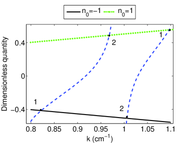
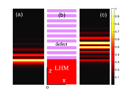
In the following, we want to discuss the effect of defect layer on the dispersion properties of the localized modes. In the used structure, we assumed that the homogeneous medium is a left-handed metamaterial (LHM) with . For comparison, we also investigated the dispersion of the corresponding localized modes in the structure, where the homogeneous medium is replaced by vacuum (). To do this, we plotted two sides of the dispersion condition (Eq. (3)) vs. in the first spectral bandgap in Fig. 1. In this figure the solid and dotted lines show the left-hand side of Eq. (3) for the cases and respectively, while the dashed lines represent the right-hand side of Eq. (3). Here we take the following values: , and . Unlike the defectless structure A. Namdar , we see that the dispersion condition has two solutions (points and in Fig. 1). So, there are two different modes for a given . To describe these modes, we plotted the intensity distribution of these modes as a function of in Fig. 2. As one can see, both of these modes are localized modes. But, the mode is localized the interface of the structure (SM) (see Fig. 2(a)), while the mode is localized at the defect layer (DLM) (see Fig. 2(c)).
. Here, and .
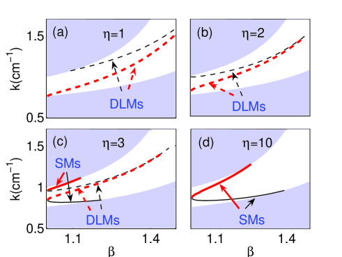
Our investigations indicate that the existence region of the SMs and the DLMs strongly depends on the position of defect layer. To show this, we plotted the dispersion curves of the localized modes in the first spectral gap as a function of for different defect position in Fig. 3. As one can see from Figs. 3(a),(b), when the position of the defect layer approaches to the surface of the structure (small ), the coupling between the incident wave and the defect mode strongly take places and leads to the formation of the DLM. But by increasing , the interaction between the incident wave and defect mode becomes weaker (see Figs. 3(c)), so that in the case of sufficiently big the DLM disappears in the benefit of the appearance of the SM. This case () corresponds to the defectless structure (see Figs. 3(d)).
In Fig. 3 we also studied the dispersion property of two different homogeneous media (i.e. LHM and vacuum). We see that when the homogeneous medium is a LHM (), the dispersion cure of the SMs settle in the near by the lower edge of the photonic bandgap and finally disappears by decreasing the distance of the defect layer from the interface of the structure. This is in contrast to the case where the LHM is replaced by the vacuum. For this case the dispersion cure of the SMs moves toward the upper edge of the photonic bandgap.
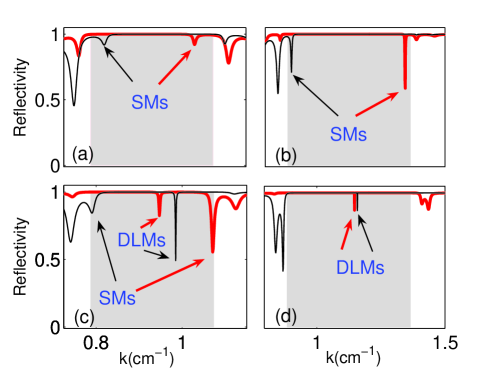
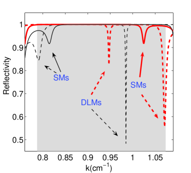
As stated in Fig. 2, the localized modes have evanescent nature and due to this evanescent nature, they will not interact directly with an incoming planewave. So, they can be excited by the ATR method. This technique has previously been invoked for the investigation of various types of surface polaritons, e.g., plasmon-polaritons in metals A. Otto ; A. Otto1 , phonon-polaritons in ionic crystals R. Ruppin ; V.V. Bryksin , exciton-polaritons in semiconductors I. Hirabayashi ; J. Lagois and magnon-polaritons in magnetic materials J. Matsuura ; M. Fukui . We consider the ATR geometry shown in Fig. 1 in reference A. Namdar1 . Here, the uniform medium represents a gap layer of the width L that separates dielectric and layered structure. For an incident angle larger than the angle of the total internal reflection, the electromagnetic field incident from an optically dense medium (dielectric) with refractive index will penetrate the gap as an evanescent wave, which can interact with the evanescent localized modes. We have calculated the reflectivity of the ATR geometry, using classical electromagnetic theory. A calculated ATR spectrum for the cases of defectless and defective multilayer structures are shown in Fig. 4 for two different incident angle (or two different ). Here, the shaded regions show the first spectral bandgap of the multilayer structure. In Figs. 4(a),(b)) there is only a deep in the ATR spectrum in the spectral bandgap corresponding to a SM. However, in Fig. 4(c) we reveal two sharp deeps in the ATR spectrum corresponding to a DLM and a SM. In Fig. 4(d), we can see only a deep in the spectral bandgap related to a DLM.
Our investigations reveal that the existence region for the SMs and the DLMs not only depends on the position of the defect layer () but also it depends on the thickness of defect layer (). To show this, we plotted the reflectivity of the ATR geometry as a function of frequency () for different thicknesses of defect layer with a fix position in Fig. 5. It is seen that for a thin defect layer, the multilayer structure behaves like as a defectless structure (see solid lines in Fig. 5) A. Namdar . Increasing the thickness of the defect layer , will push the SM to the lower (upper) edge of the bandgap in the case of () then it will disappear for the sufficiently thick defect layer, and the DLM will appear within the bandgap. In the other word, for a big the structure loses the ability to support the SMs. Therefore, the modes localize at the defect layer.
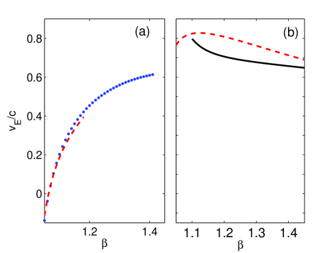
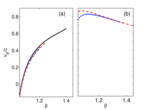
Finally, it is interest of us to know the effect of defect layer on the energy flow velocity of the localized modes. It is well known that the energy flow velocity relates total energy flow to the energy density integrated over as . We demonstrated the effect of defect position and thickness on the energy flow velocity of localized modes in the defective multilayer structure in Figs. 6 and 7, respectively. It is seen that in the presence of uniform LHM, the energy flow velocity of the SMs can be positive or negative (see Figs. 6(a) and 7(a)), which indicates the considered structure has the potential to support forward and backward energy flow (this is the noticeable advantage of using LHM). On the other hand, Figs. 6(b) and 7(b) show that the DLMs have only positive energy flow velocity. Accordingly, in the used structure the presence of LHM can not affect the direction of energy follow of the DLM. In addition, Figs. 6(a) and 7(a) reveal that the presence of defect layer can not affect considerably the energy flow velocity of the SMs, whereas the energy flow velocity of the DLMs depends on the position and thickness of defect layer (see Figs. 6(b) and 7(b)).
IV Conclusion
Briefly, we have studied the dispersion characteristics of the localized modes in the presence of defect layer in the periodic multilayer structures. It was shown that the structure can support both the SMs and the DLMs which localize at the interface of the structure and the position of the defect, respectively. Moreover, we have revealed that the existence regions of the SMs and the DLMs depend on the position and thickness of the defect layer. We show that the dispersion curves of the SMs settle near by the lower (upper) edge of the photonic bandgap for the case of the uniform medium is a LHM (vacuum), and finally disappear by decreasing the distance of the defect layer from the surface of the structure. As well, we have shown that the existence of the defect in the structure has not a considerable effect on the energy flow velocity of the SMs.
V Acknowledgment
The authors thank Prof. Yuri S. Kivshar for valuable suggestions and useful guidance.
References
- (1) Photonic Band Gaps and Localization, NATO Advanced Studies Institute, Series B: Physics, edited by C. M. Soukoulis (Plenum, New York, 1993), Vol. 308.
- (2) J. D. Joannopoulos, R. D. Meade, and J. N. Winn, Photonic Crystals: Molding The Flow of Light (Princeton University Press, Princeton, NJ, 1995).
- (3) W. M. Robertson, G. Arjavalingam, R. D. Meade, K. D. Brommer, A. M. Rappe, and J. D. Joannopoulos, Opt. Lett. 18, 528 (1993).
- (4) R. D. Meade, K. D. Brommer, A. M. Rappe, and J. D. Joannopoulos, Phys. Rev. B 44, 10961 (1991).
- (5) F. Ramos-Mendieta and P. Halevi, Phys. Rev. B 59, 15112 (1999).
- (6) J. M. Elson and P. Tran, Phys. Rev. B 54, 1711 (1996).
- (7) N. W. Ashcroft and N. D. Mermin, Solid State Physics (Saunders, Philadelphia, 1976).
- (8) P. Etchegoin and R. T. Phillips, Phys. Rev. B 53, 12 674 (1996).
- (9) F. Ramos-Mendieta and P. Halevi, Solid State Commun. 100, 314 (1996).
- (10) A. Otto, Z. Phys. 216, 398 (1968).
- (11) A. Otto, Z. Phys. 219, 227 (1969).
- (12) R. Moussa, S. Foteinopoulou, Lei Zhang, G. Tuttle, K. Guven, E. Ozbay, and C. M. Soukoulis, Phys. Rev. B 71, 085106 (2005).
- (13) C. Luo, S. G. Johnson, J. D. Joannopoulos, and J. B. Pendry, Phys. Rev. B 68, 045115 (2003).
- (14) S. Xiao, M. Qiu, Z. Ruan, and S. He, Appl. Phys. Lett. 85, 4269 (2004).
- (15) P. Kramper, M. Agio, C. M. Soukoulis, A. Birner, F. Muller, R. B. Wehrspohn, U. Gosele, and V. Sandoghdar, Phys. Rev. Lett. 92, 113903 (2004).
- (16) E. Moreno, F. J. Garcia-Vidal, and L. Martin-Moreno, Phys. Rev. B 69, 121402(R) (2004).
- (17) I. Bulu, H. Caglayan, and E. Ozbay, Opt. Lett. 30, 3078 (2005).
- (18) A. Namdar, I. V. Shadrivov, and Y S. Kivshar, Appl. phys. lett. 89, 114104 (2006).
- (19) G. V. Morozov, D. W. L. Sprung and J. Martorell, Phys. Rev. E 69, 016612 (2004).
- (20) A. Yariv and P. Yeh, Optical Waves in Crystals , Wiley (New York), (1984) Ch. 6.
- (21) J. Martorell, D. W. L. Sprung and G. V. Morozov, J. Opt. A: Pure Appl. Opt. 8, 630 (2006).
- (22) R. Ruppin, Solid. State Commun. 8, 1129 (1970).
- (23) V. V. Bryksin, Y. M. Gerbshtein, D. N. Mirlin, Sov. Phys. Solid State 13, 1779 (1972).
- (24) I. Hirabayashi, T. Koda, Y. Tokura, J. Murata, Y. Kaneko, J. Phys. Soc. Jpn. 43, 173 (1977).
- (25) J. Lagois, Solid State Commun. 39, 563 (1981).
- (26) J. Matsuura, M. Fukui, O. Tada, Solid State Commun. 45, 157 (1983).
- (27) M. Fukui, H. Dohi, J. Matsuura, O. Tada, J. Phys. C 17, 1783 (1984).
- (28) A. Namdar, I. V. Shadrivov, and Y S. Kivshar, Phys. Rev. A 75, 053812 (2007).