Lateral magnetic anisotropy superlattice out of a single (Ga,Mn)As layer
Abstract
We use lithographically induced strain relaxation to periodically modulate the magnetic anisotropy in a single (Ga,Mn)As layer. This results in a lateral magnetoresistance device where two non-volatile magnetic states exist at zero external magnetic field with resistances resulting from the orientation of two lithographically defined regions in a single and contiguous layer.
pacs:
75.30.Gw, 85.75.-d, 75.50.PpStrain control of the magnetic anisotropy in (Ga,Mn)As is currently a focus of spintronics research. Recent reports include lithographic strain control Humpfner2007 ; Wenisch2007 and related devices pappertNatPhys ; Wunderlich2007 ; RanieriCondmat , as well as the use of piezoelectric elements to electrically control the imposed strain UnottPiezoCondmat ; FurdynaPizoCondmat . So far, all of these devices imposed an homogeneous anisotropy onto the targeted structure. In this paper, we show that this process can be taken much further and demonstrate the fabrication and characterization of a lateral anisotropy superlattice. Our method involves patterning of the surface of a ferromagnetic semiconductor layer in order to allow partial strain relaxation. This is achieved by lithographically defining nanometer scale stripes into a (Ga,Mn)As layer and partially etching into the ferromagnetic layer. The unetched part of the layer remains pseudomorphically strained with its magnetic anisotropy relatively unchanged, while the stripes anisotropically relax and gain a strongly uniaxial magnetic anisotropy. By varying the depth of etching, we can control the ratio of uniaxial to biaxial anisotropy material. Our investigations reveal that for a specific ratio, the resulting structure has alternating regions of uniaxial and biaxial anisotropy, and thus constitutes a anisotropy superlattice structure.
The principle of our method is based on the nature of the ferromagnetism in (Ga,Mn)As. The magnetic interaction between the randomly distributed dilute Mn moments is mediated by itinerant holes through Zener double exchange. Because of spin orbit coupling, the wavefunction of these holes takes on anisotropies which reflect the symmetry of the lattice. When (Ga,Mn)As is grown on GaAs (001), it is compressively strained, and for the doping concentration used in our transport samples, at 4K, the primary anisotropy is an in-plane biaxial anisotropy along the [100] and [010] crystal directions Sawicki2004 . When lithographic techniques are used to trigger anisotropic deformation of the lattice along a given direction, this change in symmetry is reflected in the hole wavefunctions, and thus leads to a modification of the magnetic anisotropy.
An important distinction between the anisotropy in dilute magnetic semiconductors and traditional metals is worth noting. In metals, a common way to achieve anisotropy engineering is through shape anisotropy. However, because the strength of shape anisotropy scales with saturation magnetization, it is a relatively weak effect in (Ga,Mn)As and cannot effectively compete against the crystalline anisotropy terms. For example, the uniaxial shape anisotropy field expected Aharoni1998 from the 38 nm deep etched stripes used in this study is mT, much to small to compete with the crystalline anisotropy of mT.
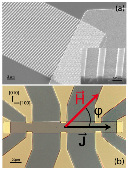
The samples are made from a typical 70 nm Ga0.965Mn0.035As layer Giselagrowth with a Curie temperature of 60 K grown on a semi-insulating (001) GaAs buffer and substrate. An array of 500 stripes of 150 nm width by 200 m length, with a period of 400 nm, and aligned along the [100] crystallographic direction, is defined by e-beam lithography into a positive bilayer resist, followed by deposition of 15 nm Ti and lift-off. This pattern is transferred into the 70 nm (Ga,Mn)As layer by chemical assisted ion beam etching (CAIBE) using the Ti stripes as a mask. By properly selecting the etching depth, we fabricate samples with stripes from to nm in thickness, leaving a continuous layer from 50 to 10 nm between the stripes. The Ti is then removed by a dip into HF:H2O (1:200). A mesa of 20 m 200 m, is defined onto the center of the array, parallel to and containing stripes, by optical lithography using a positive resist. Chemical wet etching is used to remove material around this mesa to a depth of nm into the GaAs substrate. A second optical lithographic step is then used to define Au/Ti contact pads for electrical access. Fig. 1a presents a scanning electron microscope (SEM) image of one of the ends of the 20 m wide mesa containing the stripes, where they meet the Au contact. The inset shows a close up of some of the stripes, while Fig. 1b shows the final sample layout. The resulting thickness of the stripes is determined from SEM images taken at tilted angles as well as by a stylus profiler system (Dektak 6M).
The samples are characterized by magnetoresistance studies in a magnetocryostat fitted with a vector field magnet capable of applying fields of up to 300 mT in any direction. For our purposes, the magnetic field will be confined to the sample plane, and its direction is defined with respect to the current direction flowing along the stripes. Given that the contact resistance () is negligible compared to the resistance of the stripes , a simple two terminal measurement configuration is chosen in order to maximize our sensitivity to the distribution of all the stripes instead of preferentially measuring those near the edges. We apply a constant voltage of 10 mV to the end leads of the Hall-bar and measure the resulting current in order to determine the resistance while the magnetic field is swept in the sample plane. In ferromagnetic materials the longitudinal resistance of a sample is strongly dependent on the angle between the magnetization and the current . In (Ga,Mn)As, this anisotropic magnetoresistance (AMR) Jan1957 ; MCGUIRE1975 has a resistance minimum when and a maximum when Baxter2002 .
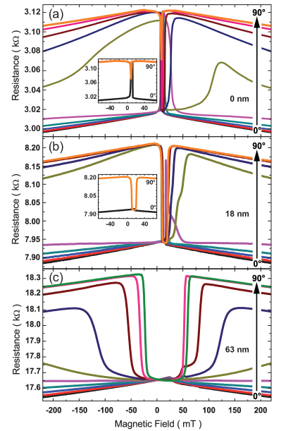
We first consider measurements on a sample with stripes of 18 nm thickness (Fig 2b). In all curves, the magnetic field is swept from -300 to 300 mT. For high magnetic fields the magnetization of the sample follows the applied external magnetic field and as expected, at 200 mT, the sample has a maximum resistance for fields along 90∘, perpendicular to , and a minimum resistance for . When decreases, the magnetization rotates towards the nearest available easy axis. For this sample, we observe that for field directions closer to 90∘, the result of this relaxation is a high resistance state, whereas for field directions nearer to 0∘ the sample relaxes to a low resistance state. At mT two stable states exist corresponding to the typical biaxial behavior of (Ga,Mn)As. After mT in all curves, magnetization reversal takes place through the nucleation and propagation of two subsequent 90∘ domain walls resulting in two distinct switching events. For reference, magnetoresistance curves on the unetched layer are shown in Fig. 2a. In such a layer, the low field features in the 0∘ and 90∘ curves are of similar width, reflecting the near symmetry of these two directions. In the layer with the 18 nm deep etched stripes, the much wider feature in the 90∘ curve and the near absence of any feature in the 0∘ curve, reveals a symmetry breaking between the two directions, highlighting a uniaxial easy anisotropy component along [100], the direction of the patterned stripes. The sample thus shows primary biaxial behavior with the uniaxial component imposed by the stripes playing only a secondary role.
The situation is reversed in Fig. 2c for the sample with stripe thickness of about 63 nm. While this sample’s behavior is similar to the first at high fields, at mT all curves converge to a single low resistance value corresponding to . The sample is now totally dominated by the uniaxial character of the stripes, and behaves as a simple uniaxial magnet.
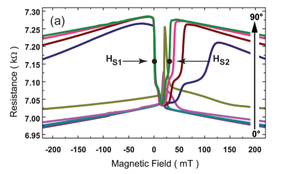
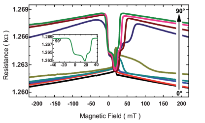
We now consider this transition from biaxial to uniaxial behavior in a sample with stripe thickness of 38 nm. Fig. 3a shows AMR measurements of such a sample. The high field behavior is again unchanged. At low magnetic fields however, when is swept in directions nearly perpendicular to , the number of switching events increases from the two distinct features observed in Fig. 2, to four distinct features. Near = 0 mT a first switching of resulting in an intermediate resistance occurs. A second switching event then follows decreasing the resistance to its minimum value corresponding to parallel to . As continues to increase the resistance changes again to an intermediate level before returning to the maximum resistance. Comparing these curves to those of Fig. 2 leads to an intuitive interpretation of what is happening: The sample breaks up into two regions having either biaxial or uniaxial magnetic anisotropy.
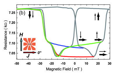
Consider the gray curve of Fig. 3b showing an enlarged view of the low field part of the = 90∘ curve, and indicating by the thick (thin) arrows the direction of magnetization of the stripes (between the stripes) regions of the sample at various point in the field sweep. At high fields, and down to -30 mT, the field aligns all moments into a uniform state . As the field is reduced, a first magnetization reorientation event occurs very near to = 0 mT, as the magnetization of the uniaxial stripes changes to an alignment along their easy axis, and thus parallel to the current. This leaves the sample in a non-trivial configuration, where the magnetization of the stripes and the regions between the stripes are orthogonal to each other. As the field is further increased to about 16 mT, the magnetization of the biaxial regions undergoes a 90∘ reorientation as part of its two step switching process. This reestablishes a co-linear, and thus low resistance state. Further sweeping of the field towards high positive value causes first the region between the stripes, and then the stripes to switch their alignment to the magnetic field direction, creating a second orthogonal state at 23 mT, and then the high resistance state where all moments are perpendicular to the current, from +30 mT onwards.
In order to verify that all these states are non-volatile, we proceed to a series of minor loops to verify their hysteretic behavior. The blue curve is obtained by sweeping the -field from -300 to 7 mT, just after the first sharp switching event, and then sweeping back to to negative fields. The sample clearly remains in the intermediate resistance state confirming that the orthogonal configuration of the magnetization in the different regions survives in the absence of magnetic field. The same is true for the second orthogonal configuration as well as the collinear low resistance state, as confirmed by the next two experiments which repeat the above procedure, but reverse field at 16 and 23 mT, at the point of emergence of each relevant state.
To confirm the robustness and reproducibility of the results presented, we have fabricated a second set of samples. The fabrication is as above, except that the Ti mask is left on the sample after processing. The sample can thus be measured for a given stripe thickness and then re-etched in CAIBE, resulting in thicker stripes that can be measured again. This allows us to investigate stripes of various thicknesses on the same piece of material, and thus ensure that the stripe thickness is the only parameter at work. Figure 4 shows measurements on the re-etched sample for a stripe thickness of 37 nm, and reproducing the mixed state behavior of Fig. 3b. In this case, because the Ti mask which is still on the sample reduced the overall device resistance, we use a four terminal measurement configuration to fully exclude any role of the contacts.
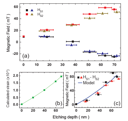
A figure of merit to quantify the strength of the imposed uniaxial anisotropy term in the stripes can be obtained from the magnetic field positions and where the resistance reaches the mid value between its minimum and maximum (see Fig. 3a), for the two uniaxial switching events in the curves of each sample NatureParabola ; Humpfner2007 . Results for both sets of samples are plotted in Fig. 5a, with the set comprised of individual samples given as squares and the set from re-etching as triangles. To within experimental determination of the stripe thickness, both sets reveal quantitatively identical behavior, and show a monotonic increase of the strength of the imposed uniaxial anisotropy as a function of increased etching depth. These results imply that the lithography is capable of controlling the relative areas of biaxial and uniaxial regions and allow for detailed engineering of anisotropic superstructures.
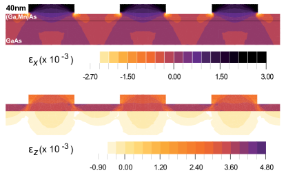
To better understand the role that strain relaxation plays in setting up this mixed stated configurations, we turn to finite element calculations. In Fig. 6a we present finite element strain simulations on a samples with 40 nm thick stripes. No strain relaxation occurs along the length of the strips, and we plot strain components perpendicular to the stripe direction () and (). = 0.00 indicates full pseudomorphic strain, where the lattice constant of the (Ga,Mn)As layer is equal to that of the GaAs substrate. For the (Ga,Mn)As lattice constant increases, indicating strain relaxation, with 10-3 corresponding to the Ga0.965Mn0.035As fully relaxing to its natural lattice constant. Negative values indicate stronger compressive strain than that of the pseudomorphic layer. The simulations clearly show that not only the stripes, but also the regions immediately under the stripe are significantly relaxed in both and directions, whereas the regions between the stripes are essentially pseudomorphic, or even partially compressively strained. This explains why the two regions have such different anisotropy properties. Moreover, the fact that the relaxed strain extends to include the material under the stripes explains why the uniaxial region carries the majority of the current, as can be established from the data of Figs. 3 and 4 where the larger of the two resistance changes occurs when the stripes change their magnetization direction.
The measurements presented in this manuscript are taken at 4.2 K. As temperature is increased, the qualitative behavior remains unchanged until about 20 K, after which the bulk layer undergoes the biaxial to [110] uniaxial anisotropy transition commonly observed in (Ga,Mn)As Sawicki2004 . The strength of the strain relaxation induced uniaxial anisotropy in the stripes shows little temperature dependence, as observed previously for this anisotropy mechanism Humpfner2007 .
Finite element calculations were carried out on stripes of various thickness, and the average strain in the striped region was extracted for each thickness. These were used as input for calculations to extract the expected value of the anisotropy strength. Following Ref.Abolfath2001 ; Dietl2001 we calculate the ground state energy of the hole system under the assumption that the magnetization is aligned along a given crystal direction. We then repeat this calculation of all possible directions of magnetization, to get a profile of the magnetic anisotropy, where the directions yielding the lowest total energy are obviously magnetically easy axes. For the strain Hamiltonian, we treat the strain in the stripes as homogeneous and given by the average value of the calculated strain in both the x and z directions (the y direction is pseudomorphic) and the off diagonal components of the strain matrix are taken to be zero. The average strain as a function of etched depth extracted from the finite element calculations, and used in the modeling are given in Fig. 5b. The other material parameters used in the modeling are as in Ref. Schmidt2007 .
Using the methods described in Ref. Wenisch2007 ; Humpfner2007 to relate the uniaxial anisotropy strength to the opening in the magnetoresistance curves, we plot as the solid line in Fig. 5c, the expected opening from the model, and compare it to the experimental values (solid symbols). Given the oversimplification in the model that the strain for each thickness can be reduced to a single homogeneous average value, the correspondence between theory and experiment is quite remarkable.
In conclusion, we have demonstrated how carefully engineered strain relaxation in (Ga,Mn)As can be used to create non trivial magnetic anisotropies within a continuous layer out of which devices can be patterned. We have used this method to demonstrate a new device functionality. The structure behaves like a two state magnetoresistance memory element, with a resistive response to the difference between two non-volatile magnetization states. Unlike previous devices where the two states differ in the relative alignment of the magnetization of separate layers, here the two regions of differing magnetization are contained within a single layer. Apart from the obvious advantages in applications, this method can also be useful for studies relying on the interplay between regions of different magnetization, such as domain wall or spin torque studies.
Acknowledgements.
The authors thank T. Borzenko and V. Hock for assistance in sample fabrication, and acknowledge financial support from the EU (NANOSPIN FP6-IST-015728).References
- (1) S. Hümpfner, K. Pappert, J. Wenisch, K. Brunner, C. Gould, G. Schmidt, L. W. Molenkamp, M. Sawicki, and T. Dietl, Appl. Phys. Lett. 90, 102102 (2007).
- (2) J. Wenisch, C. Gould, L. Ebel, J. Storz, K. Pappert, M. J. Schmidt, C. Kumpf, G. Schmidt, K. Brunner, and L. W. Molenkamp, Phys. Rev. Lett. 99, 077201 (2007).
- (3) K. Pappert, S. Hümpfner, C. Gould, J. Wenisch, K. Brunner, G. Schmidt, and L. W. Molenkamp, Nature Phys. 3, 573 (2007).
- (4) J. Wunderlich, A. C. Irvine, J. Zemen, V. Holy, A. W. Rushforth, E. De Ranieri, U. Rana, K. Vyborny, J. Sinova, C. T. Foxon, R. P. Campion, D. A. Williams, B. L. Gallagher, and T. Jungwirth, Phys. Rev. B 76, 054424 (2007).
- (5) E. D. Ranieri, A. Rushforth, K. Vyborny, U. Rana, E. Ahmed, R. Campion, C. Foxon, B. Gallagher, A. Irvine, J. Wunderlich, and T. Jungwirth, Cond-mat 08023344 (2008).
- (6) A. Rushforth, E. D. Ranieri, J. Zemen, J. Wunderlich, K. Edmonds, C. King, E. Ahmad, R. Campion, C. Foxon, B. Gallagher, K. Vyborny, J. Kucera, and T. Jungwirth, Cond-mat 08010886 (2008).
- (7) M. Overby, A. Chernyshov, L. P. Rokhinson, X. Liu, and J. K. Furdyna, Cond-mat 08014191 (2008).
- (8) M. Sawicki, F. Matsukura, A. Idziaszek, T. Dietl, G. M. Schott, C. Ruester, C. Gould, G. Karczewski, G. Schmidt, and L. W. Molenkamp, Phys. Rev. B 70, 245325 (2004).
- (9) A. Aharoni, Journal of Applied Physics 83, 3432 (1998).
- (10) G. Schott, G. Schmidt, G. Karczewski, L.W.Molenkamp, R. Jakiela, and A. Barcz, Appl. Phys. Lett. 82, 4678 (2003).
- (11) T. R. Mcguire and R. I. Potter, Ieee Transactions On Magnetics 11, 1018 (1975).
- (12) J. P. Jan, Solid State Physics ((Eds: F. Seitz, D. Turnbull), Academic Press Inc., New York, 1957), pp. Vol. 5, p.1.
- (13) D. V. Baxter, D. Ruzmetov, J. Scherschligt, Y. Sasaki, X. Liu, J. K. Furdyna, and C. H. Mielke, Phys. Rev. B 65, 212407 (2002).
- (14) F. West, Nature 188, 129 (1960).
- (15) M. Abolfath, T. Jungwirth, J. Brum, and A. H. MacDonald, Physical Review B 6305, 054418 (2001).
- (16) T. Dietl, H. Ohno, and F. Matsukura, Physical Review B 6319, 195205 (2001).
- (17) M. J. Schmidt, K. Pappert, C. Gould, G. Schmidt, R. Oppermann, and L. W. Molenkamp, Physical Review B 76, 035204 (2007).