Negative nonlocal resistance in mesoscopic gold Hall bars:
Absence of giant spin Hall effect
Abstract
We report the observation of negative nonlocal resistances in multiterminal mesoscopic gold Hall bar structures whose characteristic dimensions are larger than the electron mean-free path. Our results can only be partially explained by a classical diffusive model of the nonlocal transport, and are not consistent with a recently proposed model based on spin Hall effects. Instead, our analysis suggests that a quasiballistic transport mechanism is responsible for the observed negative nonlocal resistance. Based on the sensitivity of our measurements and the spin Hall effect model, we find an upper limit for the spin Hall angle in gold of 0.022 at 4.5 K.
pacs:
72.25.Ba, 73.23.-b, 85.35.-pThe term nonlocal resistance, , refers to the generation of a voltage in regions of a multiterminal structure that are outside of the nominal current path. In high mobility, two-dimensional semiconductor heterostructures, and magnetoresistance (MR) measurements at low temperatures provided valuable insights into understanding electron transport in the ballistic Takagaki et al. (1989); Hirayama et al. (1992) and quantum Hall regimes McEuen et al. (1990). Such measurements were also applied to study universal conductance fluctuations in diffusive semiconductors and metals in the phase-coherent regime Haucke et al. (1990), and the flow of vortices in superconducting channels Grigorieva et al. (2004). In hybrid ferromagnet/non-magnet lateral spin valve structures, nonlocal MR measurements have been utilized to study coherent spin transport phenomena, such as spin diffusion Ji et al. (2004); Jedema et al. (2003), spin precession Jedema et al. (2002), and spin Hall effects (SHEs) Valenzuela and Tinkham (2006); Seki et al. (2008). Theoretically it has also been suggested that SHEs should give rise to experimentally observable in purely paramagnetic structures when the magnitude of the spin Hall angle , defined as the ratio of spin Hall and charge conductivities, is sufficiently large Hankiewicz et al. (2004); Abanin et al. (2009). However, in this Letter, we present experimental results that show no signatures of such SHE induced in mesoscopic structures fabricated from gold, which is inconsistent with the recently reported giant in this material. We also report the surprising observation of a negative and show this to be due to a quasiballistic charge transport mechanism not related to SHEs.
Consider a Hall bar structure fabricated from a nonmagnetic normal metal, with two parallel vertical wires of width separated by a distance and bridged by a horizontal wire of identical width (see Fig. 1), and at temperatures high enough that quantum effects can be neglected. When a current runs through one vertical wire and the voltage is measured across another, a non-zero appears in the diffusive transport regime when the electron mean-free path , because the current density, which spreads into the bridging wire, has a nonzero magnitude in the region between the voltage probes [see Fig. 1(a)]. The magnitude of this classical , , decays exponentially with the distance between the wires at a rate set by the device geometry. Indeed, it follows from the van der Pauw theorem van der Pauw (1958) that for
| (1) |
where is the sheet resistance of the wire having resistivity and thickness . is positive, meaning the nonlocal voltage has the same polarity as the one along the direction of current flow in the adjacent wire.
Recently, however, an additional transport mechanism, related to SHEs, has been predicted to give rise to nonzero in a metallic Hall bar structure in the diffusive transport regime Abanin et al. (2009). This mechanism is depicted schematically in Fig. 1(b); an electrical current flowing through the left vertical wire generates a perpendicular spin current in the bridging wire due to the direct SHE. appears because the electrons carrying the spin current scatter preferentially in the same direction (inverse SHE) thus creating a charge accumulation, i.e. voltage across the right vertical wire. Abanin et al. calculated Abanin et al. (2009) that for , where is the electron spin diffusion length, this induced by SHEs, , can be expressed as
| (2) |
should also be positive (since the potential difference that builds up opposes the electron flow) and, for a given , may significantly contribute to , if and are sufficiently large. It also follows from Eq. (2) that by analyzing as a function of , one can simultaneously determine and . Compared to the experiments in which ferromagnets were used to generate or detect spin currents Valenzuela and Tinkham (2006); Seki et al. (2008), this scheme offers an advantage of avoiding complications related to spin injection or detection efficiency of the ferromagnets, which must be known in order to determine .
Motivated by these predictions, we fabricated mesoscopic gold Hall bar structures with variable distance between adjacent vertical wires and measured as a function of and temperature . Gold was chosen due to its strong spin-orbit coupling, expected to give rise to a large value, and at the same time a long enough value in order to provide a significant value of compared to . Indeed, it has been recently reported that a giant SHE exists in gold, with = 0.113 at room temperature Seki et al. (2008). Furthermore, values of of up to 168 nm at 10 K have been reported Ku et al. (2006). Surprisingly, we observed that, in addition to , the measured contains a negative contribution that decays with exponentially, as predicted by a classical model, but whose magnitude is also proportional to the fraction of electrons that can travel ballistically over the width of the bridging wire , , . A similar mechanism had been previously observed to give rise to a negative value of in structures fabricated from high mobility, two-dimensional electron systems in semiconductor heterostructures, but was typically neglected in nonlocal transport measurements on metallic nanostructures. In addition, based on Eq. (2) and the sensitivity of our measurements, we deduce , which conflicts with the recent observation of a giant SHE in gold.
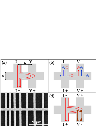
The Hall bar structures were fabricated on a SiN/Si substrate by e-beam lithography, e-beam evaporation and lift-off. A scanning electron microscopy (SEM) image of the central region is shown in Fig. 1(c). The width and the thickness of the wires were nm and nm, as determined by SEM and atomic force microscopy analysis respectively. The distance between the adjacent vertical wires was varied from 200 to 450 nm in 50 nm steps. All resistance measurements were performed by running an alternating dc current mA and measuring a dc voltage with a nanovoltmeter. The resistivity of the gold wires was 2.07 cm and 3.89 cm at 4.5 and 295 K, respectively. The corresponding values of , calculated according to the Drude formula were 40.5 and 21.6 nm, respectively, when using an electron density for gold of m-3.
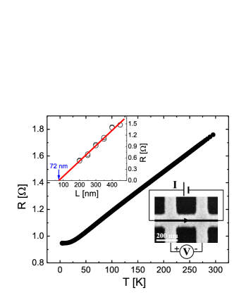
Figure 2 shows the local resistance, , measured between the two vertical wires, separated by 300 nm along the current path (see right inset), from 4.5 to 295 K. In addition to the dependence of , we also measured the resistance for each segment of the bridging wire between the adjacent vertical wires at 4.5 K. The plot of as a function of is shown in the inset of Fig. 2. As expected, increases linearly with . However, the linear fit crosses the -axis at nm, which indicates that the effective distance between the vertical wires, , is shorter than . This is most likely caused by spreading of the current density into the voltage leads, due to their finite width.
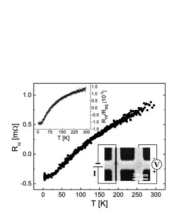
In contrast to , the dependence of the nonlocal resistance is unexpected. Figure 3 shows data obtained for nm. For other combinations of adjacent vertical wires the data show the same qualitative behavior, but different overall magnitude. At room temperature is positive, as expected based on the classical mechanism. When is lowered decreases, but this decrease is not proportional to the decrease of , as expected based on Eq. (1). This can be seen in the inset of Fig. 3 where we plot . Based on Eq. (1), should be a independent constant, determined solely by the geometry of the structure. However, we observed that is strongly dependent. Even more surprisingly, changes sign with decreasing , becoming negative around 82 K, as can be seen in the main plot of Fig. 3. The appearance of the negative rules out that the SHE mechanism, as suggested in Ref. Abanin et al., 2009, is responsible for the observed dependence of .
What transport mechanism could be responsible for the appearance of a dependent negative ? Previous numerical studies Takagaki and Ploog (1994) suggest that a negative can appear due to direct ballistic transmission of electrons into the voltage lead. This purely classical mechanism, however, is expected to be relevant only in structures fabricated from high mobility semiconductor heterostructures where exceeds characteristic dimensions of the structure. Indeed, negative has been observed in modulation doped GaAs Hall bar structures in the ballistic transport regime Hirayama et al. (1992). In order to analyze whether ballistic electrons are responsible for negative in our structures, we plot as a function of . The plots are shown on Fig. 4(a)-(f) for all distances between the adjacent vertical wires. We find that all the data can be fitted to the formula
| (3) |
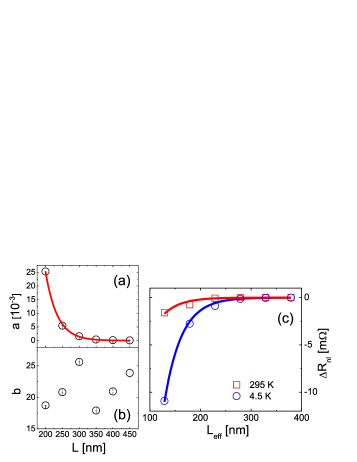
where and are dimensionless fitting parameters. Figure 5(a) shows the plot of values extracted from the fit as a function of . The fitting curve on the graph corresponds to with nm, in excellent agreement with obtained from the local resistance measurements. Therefore, in the completely diffusive limit, , we recover the classically expected with [see Eq. (1)]. In addition, it follows that the negative contribution to , since it is also proportional to , must originate from the spreading of the current density into the bridging wire. On the other hand, the term in Eq. (3) is the fraction of electrons that can travel ballistically over the distance . Thus, we conclude that the negative comes from electrons that reach the region between the voltage probes diffusively and then ballistically scatter into the lower voltage lead, generating a negative voltage. The proposed mechanism is depicted schematically in Fig. 1(d).
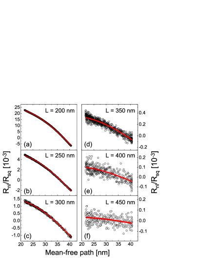
The values of extracted from fitting the curves are plotted in Fig. 5(b) for different distances . varies periodically with , which suggests that it is somewhat sensitive to the rebound electron trajectories Takagaki and Ploog (1994). The oscillatory behavior of the negative further supports the explanation that ballistic electrons are responsible for its appearance.
Finally we subtract from the measured and plot the data points as a function of for two different temperatures corresponding to the upper (295 K) and lower (4.5 K) limit of our measurement range. The data were fitted to an exponential function with fixed , where = 21.5 is the average value of , and as a fitting parameter. Both data plots and the corresponding fitting curves are shown in Fig. 5(c). We obtain nm and nm at 295 and 4.5 K, respectively. Therefore, there is no difference in the dependence of the negative on at different temperatures. One can also see that , which further confirms that the classical diffusive transport mechanism is partially responsible for the appearance of our negative values.
Thus, our experiments do not show the additional positive contribution to expected from SHEs. Mainly, such a positive contribution should manifest itself by a different dependence of on at different temperatures, due to the dependence of Kimura et al. (2008). Using the resolution of our measurements, which is 20 , and Eq. (2) with = 128.9 nm (which corresponds to shortest separation between the vertical wires in our structure) we can deduce an upper limit for of 0.022 at 4.5 K assuming nm Ji et al. (2004), and 0.027 at 295 K assuming nm. Note that the values of in both cases would be even lower if were longer. Therefore, based on our experiments, the values of are at least an order of magnitude lower than the ones reported in Ref. Seki et al., 2008. A possible reason for this discrepancy could be the recent suggestion that Fe impurities and their concomitant Kondo effect could be responsible for a giant in gold Guo et al. (2009). To this end, we note that we have not observed an upturn in the resistivity of our structures down to the lowest , which would be a signature of such a Kondo effect (see Fig. 2). Another possible reason why a giant SHE was inferred in Ref. Seki et al., 2008 could be a strong sensitivity of the nonlocal charge signal to local stray magnetic fields from ferromagnetic components of the structure Monzon et al. (1989). It is worthwhile to note that we observe significant signals, independent of spin transport, in structures with comparable geometries and dimensions as the ones studied in Ref. Seki et al., 2008, but their dependence on local magnetic fields is not clear at this point. In general, these effects, that are based only on charge transport, have been neglected in most experiments aimed at nonlocal detection of spin currents.
In conclusion, we report a negative value of in mesoscopic Hall bar structures fabricated from a nonmagnetic metal, gold. Our analysis shows that negative value arises from the effect of ballistic electrons on nonlocal transport, despite the fact that the electronic mean-free paths are smaller than the dimensions of the structure. In addition, our results do not support the recently reported giant spin Hall effect in gold.
We thank Dimitrie Culcer, Roland Winkler, Oleksandr Mosendz, and Sadamichi Maekawa for useful discussions and comments. This work was supported by DOE BES under Contract No. DE-AC02-06CH11357.
References
- Takagaki et al. (1989) Y. Takagaki, K. Gamo, S. Namba, S. Takaoka, K. Murase, S. Ishida, K. Ishibashi, and Y. Aoyagi, Solid State Commun. 69, 811 (1989); K. L. Shepard, M. L. Roukes, and B. P. Van der Gaag, Phys. Rev. Lett. 68, 2660 (1992).
- Hirayama et al. (1992) Y. Hirayama, A. D. Wieck, T. Bever, K. von Klitzing, and K. Ploog, Phys. Rev. B 46, 4035 (1992).
- McEuen et al. (1990) P. L. McEuen, A. Szafer, C. A. Richter, B. W Alphenaar, J. K. Jain, A. D Stone, R. G. Wheeler, and R. N. Sacks, Phys. Rev. Lett. 64, 2062 (1990).
- Haucke et al. (1990) H. Haucke, S. Washburn, A. D. Benoit, C. P Umbach, and R. A. Webb, Phys. Rev. B. 41, 12454 (1990).
- Grigorieva et al. (2004) I. V. Grigorieva, A. K. Geim, S. V. Dubonos, K. S Novoselov, D. Y. Vodolazov, F. M Peeters, P. H. Kes, and M. Hesselberth, Phys. Rev. Lett. 92, 237001 (2004).
- Ji et al. (2004) Y. Ji, A. Hoffmann, J. S. Jiang, and S. D. Bader, Appl. Phys. Lett. 85, 6218 (2004).
- Jedema et al. (2003) F. J Jedema, M. S Nijboer, A. T. Filip, and B. J. van Wees, Phys. Rev. B. 67, 085319 (2003); M. Johnson and R. H. Silsbee, Phys. Rev. Lett. 55, 1790 (1985).
- Jedema et al. (2002) F. J Jedema, H. B Heersche, A. T. Filip, J. J. A Baselmans, and B. J. van Wees, Nature (London) 416, 713 (2002); X. Lou, C. Adelmann, S. A. Crooker, E. S Garlid, J. Zhang, S. M Reddy, S. D. Flexner, C. J. Palmstrøm, and P. A. Crowell, Nature Phys. 3, 197 (2007).
- Valenzuela and Tinkham (2006) S. O. Valenzuela and M. Tinkham, Nature (London) 442, 176 (2006); T. Kimura, Y. Otani, T. Sato, S. Takahashi, and S. Maekawa, Phys. Rev. Lett. 98, 156601 (2007).
- Seki et al. (2008) T. Seki, Y. Hasegawa, S. Mitani, S. Takahashi, H. Imamura, S. Maekawa, Y. Nitta, and K. Takanashi, Nature Mater. 7, 125 (2008).
- Hankiewicz et al. (2004) E. M. Hankiewicz, L. W. Molenkamp, T. Jungwirth, and J. Sinova, Phys. Rev. B 70, 241301(R) (2004).
- Abanin et al. (2009) D. A. Abanin, A. V. Shytov, L. S. Levitov, and B. I. Halperin, Phys. Rev. B 79, 035304 (2009).
- van der Pauw (1958) L. J. van der Pauw, Philips Tech. Rev. 20, 220 (1958).
- Ku et al. (2006) J. Ku, J. Chang, H. Kim, and J. Eom, Appl. Phys. Lett. 88, 172510 (2006).
- Takagaki and Ploog (1994) Y. Takagaki and K. Ploog, Phys. Rev. B. 49, 1782 (1994).
- Kimura et al. (2008) T. Kimura, T. Sato, and Y. Otani, Phys. Rev. Lett. 100, 066602 (2008).
- Guo et al. (2009) G. Y. Guo, S. Maekawa, and N. Nagaosa, Phys. Rev. Lett. 102, 036401 (2009).
- Monzon et al. (1989) F. G. Monzon, H. X. Tang, and M. L. Roukes, Phys. Rev. Lett. 84, 5022 (2000); B. J. van Wees, Phys. Rev. Lett. 84, 5023 (2000).