Strong Asymmetric Effect of Lattice Mismatch on Epilayer Structure in Metal Thin Film Deposition
Abstract
We investigate the hetero-epitaxial growth of thin film deposited on a (001) substrate via molecular dynamics simulations, using six fcc transition metals as our modeling systems. By studying the radial distribution function in the film layers, we demonstrate the importance of the sign of lattice mismatch on the layer structure. For positive lattice mismatches, the film favors pseudomorphic growth, whereas for negative mismatches, a sharp transition happens within the first few monolayers of adatoms and the film layers are transformed into the close-packed (111) structure. We propose a way to quantify the compositional percentage of different planar structures in an epilayer, and demonstrate the strong asymmetric effect between the tensile and compressive cases of deposition. How temperature affects the asymmetry is also discussed.
pacs:
68.55.-a, 81.15.Aa, 68.47.De, 68.35.CtHow to epitaxially grow thin films on top of a substrate of different crystalline structure is a challenging task and continually attracts great attention of researchers due to its wide applications epitaxy04 ; ohring . It is commonly acknowledged that to grow a high-quality single-crystal film in a system where the lattice constant of the grown material and the substrate differs is very difficult. Therefore, a small lattice mismatch is generally recognized as a determinative factor for epitaxial growth, together with other factors such as surface/interface free energy, chemical bondings, temperature, etc. ohring . In hetero-epitaxial growth, an elastic strain is built up due to mismatched structure. Misfit dislocation is thus formed in the film layers to release the elastic energy while the elastic strain approaches a certain degree, which allows us to define a critical thickness of epitaxy. In the classical continuum theory frank49 ; vandermerwe63 ; matthews75 , the elastic energy is simply determined by the square of the lattice mismatch defined by where and are the unstrained lattice constants of the film and the substrate, respectively. As a consequence, the critical thickness depend only on . This is why the epitaxial growth of thin film was usually examined regardless of the sign of matthews75b ; stringfellow82 ; nix89 . Nevertheless, scientists have shown that the sign of mismatch does have a significant effect on the structure and the formation of misfit dislocations, demonstrated by experiments and numerical studies maree87 ; lu05 ; zhou06 . This effect can be attributed to the tensile-compressive asymmetry, originated from the anharmonicity of the atomic interaction trushin02&03 . Furthermore, surface energy also plays an important role in the film growth and roughening. It is known that the (111) surface has the lowest free energy for face-centered cubic (fcc) materials. Therefore, an epitaxial growth on the (100) surface for fcc metals will compete with the formation of the (111) structure. Different kinds of film structure growing on a (100) substrate have been investigated in literatures bocquet97 ; rizzi03 ; mitlin04 . Nonetheless, a systematic study of the positive and negative lattice mismatch on the structure of a film layer has rarely been conducted. The information is missed: to what degree can the tensile-compressive anharmonicity break the symmetry of the epitaxial growth predicted by the continuum theory? To answer this question, we chose six transition metals of fcc crystalline structure as our modeling systems and studied epitaxial growth of one metal on the other by means of molecular dynamics (MD) simulations. By using the radial distribution function, we were able to calculate the percentage of different surface structure in a film layer and studied the effect of lattice mismatch quantitatively.
The six transition metals that we chose are the elements Ni(3.52Å), Pd(3.89Å), Pt(3.92Å), in the group 8B, and Cu(3.61Å), Ag(4.09Å), Au(4.08Å), in the group 1B. The corresponding lattice constant kittel05 has been given, following the element symbol. We studied the thin film deposition of a metal F onto a metal S where F and S were chosen from the six elements. There are totally 36 combinations, which give the value of lattice mismatch ranging from to . We studied the film growth on the (001) plane of a substrate and denoted the system by the notation “F/S(001)”. The simulations were performed using a modified MD package, LAMMPS note-lammps , with a time step equal to 0.001 picosecond (ps). The interaction between atoms is modeled by the embedded-atom method foiles86 . The size of the substrate is of 10 unit cells in the [100] (-) and [010] (-) directions; thus, 200 atoms constitutes an atomic layer of the substrate. There are 9 atomic layers in a substrate. The atoms in the two bottom layers are fixed on the lattice positions. Above them, six layers are thermal layers subject to a temperature control by velocity rescaling method. The top layer of the substrate is free of the temperature control. Four temperatures were studied: 80K, 300K, 600K and 900K. In order to simulate an infinite surface, periodic boundary condition was applied in - and -directions.
In simulating the depositional growth, the adatoms were randomly dropped, one by one, on the top of the substrate surface, 100Å height above which, with an initial downward velocity corresponding to an incident energy 0.1 eV. This incident energy stays in the range of a typical deposition by evaporation. The deposition rate is one atom per 5 ps. Since one monolayer (ML) contains atoms in our study, the growth rate is 1 ML per nanosecond, which is several orders of magnitude higher than in molecular beam epitaxy. This choice is due to the limitation of standard MD techniques, restricted by today’s computing power. However, the high deposition rate used here does not invalidate the present study. In laser deposition techniques, such as those used in Ref. lu05 , the fluxes are relatively high, approaching to our setup. To clarify the effect of high deposition rate, we have measured the relaxation time for an adatom after collision with the surface. We found that it is less than 1 ps, consistent with theoretical predictions mccarroll63 . Therefore, the atom has enough time to relax to, at least, a local free energy minimum before coming in the next atom by this deposition rate. Another problem with high deposition rate is that there is no time for activation of many interlayer processes in film growth, such as exchange diffusion and multiple-atom concerted diffusion kellogg90 . To take into account these infrequent complex processes, more sophisticated method such as hyperdynamics or kinetic Monte Carlo simulations should be applied voter02 , where the flux can be set to a few orders of magnitude smaller than in standard MD simulations. Nevertheless, it requires much more computing resources and efforts. For a systematic study of the asymmetric effect in heteroepitaxial growth, we neglected these infrequent processes as the first-order approximation and approached this problem using standard MD simulations, in order to capture the fundamental picture of such systems. The simulation results will be benchmarked later with experimental data obtained by other groups to verify the validness of this setup. We deposited 16 monolayers (ML) of adatoms for each studied case. In order to efficiently remove the heat brought in by the adatoms, the thermal layers were extended upward, one layer by one layer, each time when one ML of adatoms has been deposited onto the surface.
We first studied the Cu/Ni system. The mismatch is . The negative mismatch means that the film suffers from a compressive strain. We monitored the coverage of each epilayer during deposition by where is the number of adatoms in the -th epilayer while ML of adatom has been deposited. The results are shown in Fig. 1 at three temperatures: 80K, 300K and 600K.
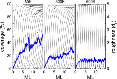
is zero at beginning. It rapidly increases, one layer after another, and saturates to some value. For the first few layers, this value is nearly , which indicates a good coverage. However, as increases, saturates to a value significantly small then 1, suggesting the formation of voids in the high epilayers. We found that the higher the temperature, the less the voids will be formed. It can be attributed to the high kinetic energy of the adatoms due to the high substrate temperature. With high kinetic energy, the adatoms can easily overcome energy barrier and migrate to the voids, flattening the film with good coverage. At 600K, the layer coverage is nearly and no void is formed in the epilayers. Moreover, only a single curve increases at any given moment at this temperature. The film thus grows layer by layer; it is the Frank-van der Merwe growth mode. On the other hand, at 80K and 300K, following the layer-by-layer growth, several curves increases at the same time. The system undergoes a wetting-layer and island-growth mode, or Stranski-Krastanov growth mode.
We also calculated the real-time roughness of the film surface. The definition of is the square root of the variance of the height of the atoms homogeneously sampling on the surface. The results are plotted in Fig. 1 in thick curves in unit of the thickness of a film layer. It clearly shows that the roughness is reduced by increasing temperature. At 80K, is about after deposition of 16 ML, because of the island growth; but at 600K, it is ca. , owing to the flat-film growth. We have examined other systems, such as Pt/Cu () and Pd/Ni (). The results showed similar trends of behavior: the coverage and the surface flatness are both improved by increasing the substrate temperature.
We then investigated the structure of thin film after deposition by analyzing the two-dimensional radial distribution function (2D RDF) of each epilayer. The 2D RDF is calculated by , where is the surface density of adatom in the th epilayer at a radial distance away from an adatom, and is the average surface density in the epilayer. In order to study the tensile-compressive asymmetry, for the two counter-systems, Pd/Cu () and Cu/Pd (), at 300K were calculated. The results are illustrated in Fig. 2.
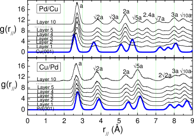
Focus firstly on the tensile case, Cu/Pd. The referenced curve for the Pd substrate surface shows the standard 2D RDF for a (001)-plane in which the peaks appear subsequently at the positions , , , , etc., with being the nearest atomic distance. We have verified that the integration of these peaks with the appropriate weight reproduces, respectively, the numbers of the nearest, the next nearest, the 3rd nearest neighbor atoms, and so forth. We found that the Cu epilayers display a similar to the structure of Pd surface. It suggests a pseudomorphic growth of thin film along the [001]-direction. Since atomic spacing of Cu is smaller than Pd, the peaks in the Cu epilayers move slightly toward left, as increasing the layer number, to reduce the strain. It approaches the bulk spacing Å of copper at the 10th epilayer.
Focus secondly on the counter system, Pd/Cu. The Pd epilayers now suffer from compressive strain and release the strain by dislocation or alternating the film to a close-packed structure. Dramatic change in the structure was observed, compared to the previous case. The change includes the change of the peak height and the appearance of some new peaks in reference of the 2D RDF of the Cu substrate. Note that a new peak appears at since the 2nd epilayer. It strongly suggests a hexagonal arrangement of atoms because the typical 2D RDF for a hexagonal lattice shows a series of peaks at the positions , , , , and so on. Therefore, the epilayers take a mixed structure combining the (001)- and the (111)-planes. Recent experimental study lu05 showed that the tensile overlayer for Cu/Pd(100) remains coherent up to about 9 ML, whereas for Pd/Cu(100), misfit dislocation appears just after few ML. To make a comparison with the experiments, we calculated in Fig. 3 the in-plane lattice strain (defined as ) and the interlayer distance of film during the growth process.
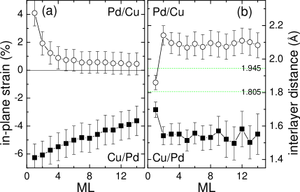
We observed the striking asymmetric behavior in the relief of in-plane strain: the compressive strain relaxes within just few ML, much more quickly than the tensile strain does. This is in agreement with the experiments lu05 . For interlayer distance, a sudden increase appears for the Pd/Cu system while the film grows more than one ML. This is because Pd has larger lattice constant than Cu; therefore, the distance between the Cu-Pd interface is smaller than the Pd-Pd epilayer distance inside the film. Similar argument can also explain the sudden decrease of the interlayer distance at one ML for the Cu/Pd system. Moreover, the interlayer distance inside the Pd film is about 2.1Å. This value is larger than Å, the layer distance of a bulk palladium along the [001] direction, but smaller than Å, the distance along the [111] direction. Since the in-plane strain relaxes quickly in this case, this intermediate value reflects the fact of the formation of film layers, each of which takes a mixed planar (001)- and (111)-structure. On the other hand, the interlayer distance inside the Cu film is smaller than Å, half of the lattice constant of copper. Since Cu film grows pseudomorphically on Pd(001) substrate, this small value indicates the falling-down of an epilayer above another epilayer inside the film due to the unrelieved strain which has a in-plane lattice constant larger than the bulk one. The interlayer distance is therefore reduced. Scientists lu05 have observed exactly what we found here. Our results show good agreements with experiments in many aspects, more than qualitatively, although the deposition rate is fast. This gives a direct support to our simulations and the standard MD techniques can capture the main trend of behavior of this kind of systems and provide valuable information and insight into the problems.
In order to have a direct image of the deposited layer structure in mind, we present in Fig. 4 the snapshots of the 10th epilayer for the two systems.
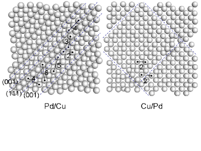
The Pd epilayer shows lattice displacement along the diagonal ([110]) direction to reduce compressive strain, resulting in a series of structural changes between (001)- and (111)-planar structures, in form of strips. In the snapshot, some typical atomic distances, which contribute the peaks in the RDF in Fig. 2, are plotted and marked by the peak number. For example, the 2nd and the 5th peaks in are derived from the atoms in the (001)-planar strips, with the atomic arrangements similar to the links marked by 2 and 5, respectively, in the picture; the 3rd peak comes from the arrangement in the (111)-planar strips, similar to the link 3. The links across the boundary of the (001)- and (111)-planar strips contribute other peaks not appeared in the standard RDFs, such as the peak at which is due to the link 6. The link 4’ is across the strip boundary and has the length . Nonetheless, lattice vibration at 300K smears the peak out, which becomes indistinguishable with the 4th peak at position .
The 10th epilayer for the Cu/Pd system shows much simpler structure, basically following the structure of the (001)-plane. It is an epitaxial growth. However, the epilayer feels tensile strain due to the Pd substrate. The strain is relaxed by creating breaks in the diagonal directions, separating the film layer into domains. This kind of rectangular domains has been experimentally observed lu05 ; mitlin04 . Moreover, we found that some atoms can sit on the breaks with the atom height deviating of the layer, which results in the small hump in the RDF curve near Å. For a link across a domain boundary, like the link 2’, the length of the link is larger than the link inside a domain, like link 2. It is why small humps additionally appear in the RDF in Fig. 2, for e.g., at Å and at other places.
Paniago et al. paniago04 have studied the stress relaxation by monitoring the RHEED pattern of the growth of Pd film on Cu(111) substrate. They found a quick increase of atom spacing with layer number during deposition, and the pseudomorphic growth was only up to the 2nd film layer. Our Pd/Cu system shows consistent results. Since our substrate surface is the (001)-plane but not the (111)-plane as used in their experiment, one more option exists for the film to relax the strain by transforming the structure into the close-packed one. We have verified other systems with smaller compressive strain, for example, the Cu/Ni () system. The film layer turns to follow basically the structure of the nickel. These findings demonstrate the importance of lattice mismatch on thin film deposition in pseudomorphic growth and in determination of the structure of epilayer.
Known that an epilayer can take a mixed structure while depositing onto a (001)-plane, an important question to be answered is to quantify the percentages of the (001)- and the (111)-planar structures in an epilayer and to study how they depend on the lattice mismatch. We propose the following method to achieve this goal. The peaks at and in can serve as an unambiguous identifier to identify, respectively, the (001)- and the (111)-planar structures, contributed from the next nearest neighboring atoms. By integrating the two peaks separately with weighting , we calculated the mean numbers of the adatoms in an epilayer with a distances and , respectively, to an adatom. The percentages of the two structures were then computed by dividing the two mean numbers separately by 4 and by 6, which are, in turn, the numbers of the next nearest neighbors for a perfect (001)- and a perfect (111)-structure. Subtracting these two percentages from 1 gives the percentage for the other structure. The results, averaged from the 5th to the 10th epilayer, which excludes the possible interface alloying region, are shown in Fig. 5 as a function of lattice mismatch at three temperatures 80K, 300K and 900K.
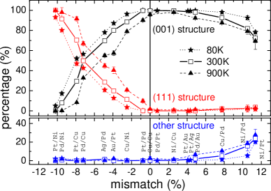
We observed an asymmetric curve with respect to . When is negative, the percentage of the (001) structure decreases enormously with increasing ; at the same moment, the percentage of the (111) structure increases. Nearly no atom sits on a site other than the two structures. The results shows that for a large mismatch, such as the Pt/Ni system (), the film layers tend to grow a close-packed structure to reduce the compressive strain, instead of epitaxially following the square lattice of the substrate surface. On the other hand, for a positive lattice mismatch, the percentage of the (001)-structure also decreases with , but more weakly compared to the systems with negative mismatch. In this case, the formation of the (111)-film structure will not be helpful to reduce the tensile strain; thus, almost no close-packed structure is formed. The strain is relaxed by the creation of breaks on the film layers. The adatoms sitting on the breaks (cf. Fig. 4) contribute the percentage of the other structure. This tensile-compressive asymmetry has been emphasized and discussed in recent studies lu05 .
Concerning the effect of temperature, we found that the higher the substrate temperature, the less the film will grow in a pseudomorphic way; in other words, the percentage of the (001)-film structure decreases. This effect is more obvious in the regime of negative mismatch than positive one. For positive mismatches, the percentage of other structure also increases with temperature. We know that the (111) plane has the lowest surface energy for fcc metals. Increasing temperature enhances the migration of an adatom to a more thermodynamically stable site, the site on the (111) plane. A negative misfit will promote this migration to form a close-packed structure to reduce the mechanically compressive strain, whereas a positive misfit will hinder it because it increases the tensile strain which is mechanically unfavorable. The interplay between the thermodynamics and the mechanics of the materials determines the film structure.
For the implication to experiments, this study suggests that it is easier to grow pseudomorphic film on (001) surface of these transition metals in the positive region of lattice mismatch than in the negative. We also emphasize that the method proposed in this study to quantify the structural composition can be adapted to experiments because the 2D RDF of a film layer can be experimentally obtained by surface diffraction techniques. Thus the structural composition versus lattice mismatch can be calculated to understand this strong asymmetry predicted by our simulations. Concerning the limitation of the standard MD techniques, it is definitely worth in the future to investigate the effect of the neglected interlayer diffusion processes on this problem using more sophisticated simulation techniques.
In summary, we have discussed the effect of lattice mismatch on the structure of epilayers on the (001) substrate surface among six transition metals. The layer coverage, the surface roughness, and the temperature effect have also been studied. We presented the first calculation of the composition percentage of film structure for positive and negative lattice mismatches. The results revealed a strong asymmetric behavior between the tensile and the compressive cases. The epilayer releases compressive strain by the formation of the close-packed planar structure, but release tensile strain by the creation of breaks and domains on a film layer.
This work is supported by the National Science Council, the Republic of China, under the contract No. NSC 95-2112-M-007-025-MY2. Computing resources are supported by the National Center for High-performance Computing.
References
- (1) M. A. Herman, W. Richter, and H. Sitter, Epitaxy : Physical Principles and Technical Implementation (Springer-Verlag, Berlin, 2004).
- (2) M. Ohring, Materials Science of Thin Films (Acedemic Press, New York, 2002), 2nd ed.
- (3) F. C. Frank and J. H. Van der Merwe, Proc. R. Soc. A 198, 216 (1949).
- (4) J. H. Van der Merwe, Appl. Phys. 34, 123 (1963).
- (5) J. W. Matthews, in Epitaxial Growth Part B, p560, J. W. Matthews, ed., (Academic Press, New York, 1975).
- (6) J. W. Matthews and A. E. Blakeslee, J. Cryst. Growth 29, 272 (1975).
- (7) G. B. Stringfellow, Rep. Prog. Phys. 45, 469 (1982).
- (8) W. D. Nix, Metall. Trans. 20A, 2217 (1989).
- (9) P. M. J. Marée, J. C. Barbour, J. F. van der Veen, K. L. Kavanagh, C. W. T. Bulle-Lieuwma, and M. P. A. Viegers, J. Appl. Phys. 62, 4413 (1987).
- (10) Y. Lu, M. Przybylski, O. Trushin, W. H. Wang, J. Barthel, E. Granato, S. C. Ying, and T. Ala-Nissila, Phys. Rev. Lett. 94, 146105 (2005).
- (11) N. Zhou and L. Zhou, Mater. Chem. Phys. 100, 168 (2006).
- (12) O. Trushin, E. Granato, S. C. Ying, P. Salo, and T. Ala-Nissila, Phys. Rev. B 65, 241408(R) (2002); Phys. Rev. B 68, 155413 (2003).
- (13) F. Bocquet, S. Robert, S. Gauthier, J. L. Duvault, and J. Klein, Surf. Sci. 392, 86 (1997).
- (14) G. A. Rizzi, M. Petukhov, M. Sambi, and G. Granozzi, Surf. Sci. 522, 1 (2003).
- (15) D. Mitlin, A. Misra, V. Radmilovic, M. Nastasi, R. Hoagland, D. J. Embury, J. P. Hirth, and T. E. Mitchell, Phil. Mag. 84, 719 (2004).
- (16) C. Kittel, Introduction to Solid State Physics (Wiley, U.S.A., 2005), 8th ed.
- (17) S. J. Plimpton, J. Comp. Phys. 117, 1 (1995); LAMMPS web site: http://lammps.sandia.gov.
- (18) S. M. Foiles, M. I. Baskes, and M. S. Daw, Phys. Rev. B 33, 7983 (1986).
- (19) B. McCarroll and G. Ehrlich, J. Chem. Phys. 38, 523 (1963).
- (20) G. L. Kellogg and P. J. Feibelman, Phys. Rev. Lett. 64, 3143 (1990); T. R. Linderoth, S. Horch, L. Petersen, S. Helveg, E. Lægsgaard, I. Stensgaard, and F. Besenbacher, Phys. Rev. Lett. 82, 1494 (1999); H. Jósson, Annu. Rev. Phys. Chem. 51, 623 (2000).
- (21) A. F. Voter, F. Montalenti, and T. C. Germann, Annu. Rev. Mater. Res. 32, 321 (2002).
- (22) R. Paniago, A. de Siervo, E. A. Soares, H.-D. Pfannes, and R. Landers, Surf. Sci. 560, 27 (2004).