Diameter-dependent electronic transport properties of Au-catalyst/Ge-nanowire Schottky diodes
Abstract
We present electronic transport measurements in individual Au-catalyst/Ge-nanowire interfaces demonstrating the presence of a Schottky barrier. Surprisingly, the small-bias conductance density increases with decreasing diameter. Theoretical calculations suggest that this effect arises because electron-hole recombination in the depletion region is the dominant charge transport mechanism, with a diameter dependence of both the depletion width and the electron-hole recombination time. The recombination time is dominated by surface contributions and depends linearly on the nanowire diameter.
pacs:
72.20.Jv, 73.63.Rt, 85.35.-pSemiconductor nanowires show promise as active elements in electronic dai ; yang , optoelectronic duan ; samuelson , and sensing lieber devices. Often, metal-catalyzed chemical vapor deposition is used to grow the nanowires, with Au the most frequent catalyst metal. Typically, a small hemispherical Au particle remains attached on the tip of the nanowires after the growth is ceased kodambaka . To date, the electrical nature of the Au-catalyst/nanowire junction remains largely unknown. Yet, there are several scientific and technological reasons to explore the electronic transport characteristics of such contacts. For example, catalyst/nanowire junctions offer a unique opportunity to examine how nanoscale dimensions affect contact properties; and rectifying contacts to free-standing, vertically oriented nanowires could prove useful in a number of applications such as Schottky detectors and mixers.
Here, we use a microprobe inside of a scanning electron microscope (SEM) to examine the charge injection at Au-catalyst/Ge-nanowire interfaces and subsequent transport in the Ge nanowire. Our measurements indicate that this interface is rectifying with a large Schottky barrier. Remarkably, the current density increases with decreasing nanowire diameter, in contrast to common expectations. By modeling the nanowire electrostatics, we show that this arises because the current is dominated by electron-hole recombination in the depletion region, a contribution which is usually negligible in bulk junctions, but is strongly enhanced in nanowires due to the increased importance of surface recombination. Combining the modeling results with the experimental data, we find that the recombination time decreases as the nanowire diameter is decreased; a simple theory including bulk and surface recombination explains this result.
The growth of Ge nanowires was performed in a cold wall chemical vapor deposition system by the vapor-liquid-solid techniquedailey at a temperature 375 ∘C and total pressure of 1.5 Torr. A 30% GeH4 precursor in H2 along with 100 ppm PH3 in H2 as the source of the n-type dopant was used with the gas flows set for a 1.2 x10⁻³ P to Ge atom ratio. Au colloids were used as the catalytic growth seeds on heavily doped (0.06-cm) n-type Ge (111) substrates with acidified deposition of the colloids immediately prior to introduction into the growth chamber to achieve predominately vertical nanowire growth. Based on previous resultswang ; tutuc , we estimate that the carrier concentration is on the order of 10cm-3.
The electrical measurements were carried out by contacting individual vertically-oriented nanowires directly on the growth substrate using a piezomotor controlled, Au-coated W probe retrofitted inside of a JEOL SEM and connected to an Agilent semiconductor parameter analyzerstatistics . A SEM image of the probe near as-grown Ge nanowires is shown in the inset of Fig. 1a. Most nanowires are 100 nm in height and have diameters from 20-150 nm (2 nm). Virtually all of the nanowires are capped with the hemispherical Au catalyst nanoparticle.
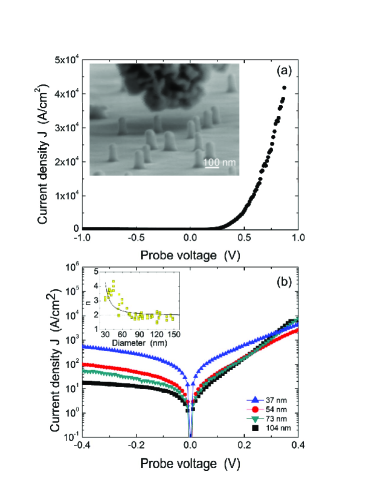
The current-voltage characteristics of a nanowire of 54 nm diameter is shown in the main panel of Fig. 1a. The behavior is clearly rectifying, as observed in almost all of the nanowires. This rectifying behavior is consistent with that observed at bulk Au/Ge interfaces nishimura , where a large Schottky barrier of 0.59 eV is present, and is essentially independent of the type of metal because Ge has strong Fermi level pinning close to the valence band. Our observations are also consistent with atom-probe tomography measurements lauhon and with high-resolution transmission electron microscopypicraux which indicated an abrupt interface between the Au catalyst nanoparticle and the Ge nanowires. It is tempting to analyze the rectifying behavior using conventional thermionic emission theory to extract the Schottky barrier. However, a surprising observation does not fit into existing theories of electronic transport through Schottky barriers.
The observation, as shown in Fig. 1b, is that the small-bias conductance density and reverse-bias current density are found to depend strongly on the nanowire diameter, and in fact, increase with decreasing diameter. This is contrary to most models of transport in nanowires, where the increased importance of surface scattering reduces the small-bias conductance density when the diameter is decreased. In addition, the phenomenon cannot be explained based on a reduction of the effective Schottky barrier height due to increased tunneling at smaller dimensions because the depletion width actually increases with decreasing diameter, as we will show below. To understand the experimental observations, and why the current-voltage characteristics of Fig. 1b cannot be analyzed using thermionic emission theory, we first consider the total current density in a Schottky diode; this can be written as , where is the thermionic current density, is the electron-hole recombination current density in the neutral region, and is the electron-hole recombination current density in the depletion region. The first contribution is of the form sze with the Richardson constant, the Schottky barrier height, the applied voltage, Boltzmann’s constant, and temperature. In most diodes, this term dominates the behavior. In the present case however, this contribution is negligible because of the large Schottky barrier of 0.59 eVbarrier ; indeed, the small-bias conductance due to this term, , is much smaller than that measured experimentally . Similarly, the second term sze , with the carrier mobility, the intrinsic carrier concentration, the dopant concentration, and the electron-hole recombination time, gives a negligible small-bias conductance even with very low values of the recombination time. Thus, we are left with the contribution sze
| (1) |
where depends on the depletion width and . By analyzing the curves of the nanowires with the functional form , we extract an ideality factor for the larger nanowires as shown in the inset of Fig. 1b, in agreement with Eq. . This suggests that electron-hole recombination in the depletion region is the dominant transport mechanism in these nanoscale contacts. (The reason for the larger values of at smaller diameters will be discussed below.)
To further explore the role of electron-hole recombination, we performed calculations of the small bias conductance of Ge nanowires. The small-bias conductance density is written assze
| (2) |
where and are the electron and hole concentration at position along the nanowire of length . In anticipation of the results below, we have written the recombination time as being diameter dependent. The term inside of the integral corresponds to the local recombination rate, assumed to be independent of the radial coordinate, an assumption that is supported by our three-dimensional calculations that we now describe.
To obtain the carrier concentrations and , we calculate self-consistently the charge and the electrostatic potential at zero bias for the geometry of Fig. 2. There, a Ge nanowire of diameter , length 100 nm, and dielectric constant is making contact to a bulk metal on one side and to the Ge substrate on the other side. A cylindrical protrusion from the bulk metal with diameter and length equal to the nanowire diameter was included to simulate the metallic nanoparticle. The nanowire is surrounded by vacuum and is uniformly n-doped with dopant concentration of 10 (this choice of the dopant concentration will be justified based on the results below). We numerically solve Poisson’s equation using finite-difference, with the spatially varying charge on the nanowire and with appropriate boundary conditions: at the metal/nanowire interface, the strong Fermi level pinning fixes the electrostatic potential to give a Schottky barrier of 0.59 eV, while at the nanowire/substrate interface the potential is fixed to give charge neutrality for a doping of 10. Boundary conditions are also applied at the nanowire surface to produce the electric field discontinuity due to the different dielectric constants of the nanowire and vacuum, and far away from the nanowire (1 micron in practice) the radial electric field vanishes. The local charge in the nanowire is calculated by integrating the bulk density of states for Ge (shifted by the local electrostatic potential) times the Fermi function at room temperature, . We also consider the fact that Ge nanowire surfaces contain a large density of surface statesdai . We thus include an additional contribution to the charge given by ; this represents surface states of uniform density in the Ge bandgap, with a neutrality level at midgap; they decay exponentially into the nanowire with a decay length nm, and have a density at the surface states/eV/atom (our conclusions are unchanged even if we vary this surface state density by an order of magnitude). Finally, the electrostatic potential and the charge are obtained self-consistently using Pulay mixing on Poisson’s equation and the expressions for and .
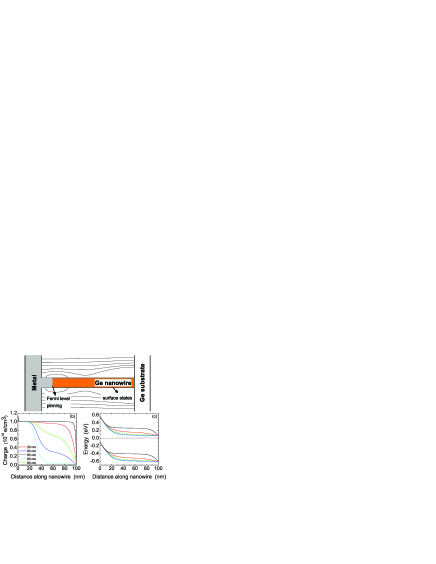
Figure 2 shows the calculated self-consistent charge and band-bending for nanowires of different diameters. Near the metal/nanowire interface, the nanowire is of p+ character due to the position of the Fermi level close to the valence band. A depletion region then extends over a length that increases strongly as the nanowire diameter is decreased. As a consequence, the total recombination current density in the depletion region increases with decreasing diameter. To see if this behavior is sufficient to explain our experimental data, we calculated the small bias conductance from Eq. assuming a fixed recombination time chosen to reproduce the large diameter values. When compared with the experimental data in Fig. 3, the calculated small bias conductance with the diameter-independent recombination time (dashed line) provides some increase with decreasing diameter, but is insufficient to give the amount of measured current and to reproduce the strong diameter dependence observed experimentally. Thus, we conclude that the total recombination time must depend on the nanowire diameter. To extract it from our experimental data, we fit the calculated recombination current density to the experimental data in Fig. 3 using a diameter-dependent recombination time ; this gives excellent agreement with the measurements as shown by the solid line in Fig. 3, with the value .
To understand the dependence of the recombination time on nanowire diameter, we consider an infinitely long nanowire into which carriers of density are injected initially. These carriers relax by diffusing through the nanowire and recombining at the surface and in the bulk. Their time and spatial dependence satisfy the diffusion equation mckelvey where is the diffusion constant. At the nanowire surface, electron-hole recombination with surface recombination velocity takes place, giving the boundary condition mckelvey . The solution of these equations gives an exponential time decay of the carrier density, with the smallest time constant where satisfies
| (3) |
with a Bessel function of order . For (which applies to our data), one can use the small argument behavior of the Bessel functions in Eq. to get and
| (4) |
Thus, the total recombination time is reduced by the presence of the surface term. From our fit to the experimental data in Fig. 3, we extract ; this value is consistent with that recently measured on similar Ge nanowires using ultrafast time-resolved optical measurements rahid . (The theory predicts in the limit , and this could be fitted to the data of Fig. 3. However, this leads to a value for that is two orders of magnitude lower than typical values for Ge.)
The dominance of electron-hole recombination in this system also explains the large ideality factors measured at forward bias for the smaller nanowires. Because the recombination current is essentially an integration over the depletion regionsze , , where the bias dependence of arises because the built-in potential is reduced to at forward bias. In bulk diodes, this leads to a mild dependence , with little impact on the ideality factor. However, for a nanowire depends exponentially on the applied voltage, as we now discuss.
To calculate the depletion width, we approximate the charge distributions in Fig. 2b as for , where is the nanowire depletion width. The electrostatic potential at the center of the wire is then , where is the electrostatic Green’s function with the boundary conditions that the derivative of the potential at the nanowire surface be discontinuous by the ratio of dielectric constants of the environment and nanowire; also includes the contribution from image charges in the metal, and can be obtained using standard techniques. With the requirement that at the edge of the depletion layer give the built-in voltage this allows us to obtain (in the limit )
| (5) |
This relationship is similar to that obtained for carbon nanotubes leonard .

The exponential dependence of explains the large forward bias ideality factors shown in the inset of Fig. 1b. Indeed, we have giving with
| (6) |
Thus, the ideality factor increases as the nanowire diameter is reduced below the length scale . This behavior can be tested by numerically fitting the data in the inset of Fig. 1b. As shown by the solid line, this provides a good description of the measured ideality factor with the value ; this compares reasonably with the value of predicted by the expression for . (We note that at reverse bias, the depletion width should increase exponentially with voltage, explaining the lack of saturation observed in our measurements. But because increases so rapidly, it can quickly reach the finite length of the nanowire and start to deplete the substrate, leading to a more complicated dependence on voltage. However, it is clear from Fig. 1b that the reverse bias current density increases more strongly as the diameter is reduced.) As mentioned earlier, the expected carrier concentration is in the range 10 cm-3; our results suggest that the doping is actually close to the lower end of this range. Indeed, for a doping of cm-3, the calculated depletion width is only 10 nm and does not vary over the experimental diameter ranges. Thus, the condition is not satisfied, and the exponential dependence of on voltage originating from Eq. would not occur and the ideality factor would be independent of diameter.
To summarize, the unusual diameter-dependent electronic transport in this system originates from several effects: Fermi level pinning at the Au/Ge interface gives a large Schottky barrier and negligible thermionic current. As a consequence, electron-hole recombination in the depletion region dominates the current. This recombination current increases as the nanowire diameter is reduced because the depletion width increases with decreasing diameter, but mostly because the recombination time decreases due to the added importance of surface recombination. At forward bias, the ideality factor increases with decreasing diameter due to the electrostatics at reduced dimensions. More generally, our results suggest that the electronic transport properties of nanoscale contacts can differ significantly from those of their bulk counterparts.
We thank D. Kienle for contributions to the self-consistent computational approach. Work performed in part at the U.S. Department of Energy, Center for Integrated Nanotechnologies, at Los Alamos National Laboratory and Sandia National Laboratories.
∗email:fleonar@sandia.gov
References
- (1) D. Wang et al., J. Am. Chem. Soc. 126, 11602 (2004).
- (2) J. Goldberger et al., Nano Lett. 6, 973 (2006).
- (3) X. Duan, et al., Nature 409, 66 (2001).
- (4) H. Pettersson et al., Nano Lett. 6, 229 (2006).
- (5) G. Zheng et al., Nat. Biotechnol. 23, 1294 (2005).
- (6) S. Kodambaka et al., Phys. Rev. Lett. 96 096105 (2006).
- (7) J.W. Dailey et al., J. Appl. Phys. 96, 7556 (2004).
- (8) Y. Wang et al., Nano Lett. 5, 2139 (2005.
- (9) E. Tutuc et al., Appl. Phys. Lett. 89, 263101 (2006).
- (10) Two to four measurements were taken for each nanowire, by retracting the tip and re-contacting the nanowire. The I-V curves were essentially identical, and the reported data is the average. This also implies that the SEM imaging did not change the properties of the nanowires.
- (11) T. Nishimura, K. Kita, and A. Toriumi, Appl. Phys. Lett. 91, 123123 (2007).
- (12) D.E. Perea et al., J. Solid State Chem. 181, 1642 (2008).
- (13) J. L. Taraci et al., App. Phys. Lett. 84, 5302 (2004).
- (14) S. M. Sze, Physics of semiconductor devices, (Wiley, New York 1980).
- (15) The Schottby barrier depends on atomic details of the Au/Ge interface; at the nanowire sizes considered here, we expect a value similar to that of bulk interfaces.
- (16) J.P. McKelvey and R.L. Longini, J. Appl. Phys. 25, 634 (1954).
- (17) R.P. Prasankumar et al., Nano Lett. 8, 1619 (2008).
- (18) F. Léonard and J. Tersoff, Phys. Rev. Lett. 83, 5174 (1999).