Atomistic simulations of self-trapped exciton formation in silicon nanostructures: The transition from quantum dots to nanowires
Abstract
Using an approximate time-dependent density functional theory method, we calculate the absorption and luminescence spectra for hydrogen passivated silicon nanoscale structures with large aspect ratio. The effect of electron confinement in axial and radial directions is systematically investigated. Excited state relaxation leads to significant Stokes shifts for short nanorods with lengths less than 2 nm, but has little effect on the luminescence intensity. The formation of self-trapped excitons is likewise observed for short nanostructures only; longer wires exhibit fully delocalized excitons with neglible geometrical distortion at the excited state minimum.
I Introduction
Research on silicon nanowires (SiNW) has intensified in the past years, owing to their potential applications in future nano-technologies, such as nanosensors Cui2001 , nanoscale electronics and photonics devices.Cui2001a ; Gudiksen2002 ; Duan2003 This interest results from the electronic structure of SiNW beeing critically dependent on the size, orientation, passivation and doping level of the nanostructure. For example, it has been shown experimentally that the band gap can be tuned by choosing different growth directions and diameters for the wire.Ma2003 On the theoretical side, the ground state electronic structure and transport properties of different kinds of SiNW have been investigated by several authors.Zhao2005 ; Zhang2005 ; Ponomareva2005 ; Yan2006 ; Bruno2007 ; Aradi2007 ; Rurali2007
Light absorption and emission of these systems have also attracted great attention, because the band gap in bulk crystalline Si is small and indirect, while that in SiNW can become large and direct due to the quantum confinement effect.Wolkin1999 ; Yu1999 ; Li2002 ; Lyons2002 ; Guichard2006 This experimental progress paves the way to obtain visible light from silicon materials, and provides for the possibility of future optoelectronics applications. In the past, theoretical descriptions of the optical properties of SiNW were mainly restricted to determining their absorption spectrum.Zhao2005 ; Bruno2007 ; Aradi2007 To quantify luminescence, it is often tacitly assumed that de-excitation occurs resonantly. However, absorption and emission spectra can differ considerably due to excited state relaxation, and simulations that take this Stokes shift into account are currently missing for SiNW.
II Method and Simulation Approach
In this letter, we use the time-dependent density-functional based tight-binding (TD-DFTB) method Niehaus2001a (for a recent review see Niehaus2009 ), to study the excited states and optical properties of SiNW. The same method has been applied to silicon quantum dots, Wang2007 ; WangZLNF2007 ; LiZNFL2007 ; WangZLFN2008 ; LiZLNF2008 ; LiZLNF2008_2 ; LiZNFL2007_2 where it was found to provide a high degree of reliability and computational efficiency compared with the parental time-dependent density functional theory (TD-DFT) from which it is derived. For example, the optical gap of Si5H12 is predicted to be 6.40 eV, in very good agreement with the experimental value of 6.50 eV.Feher1977 Also for larger clusters like Si35H36, the TD-DFTB estimate for the lowest allowed singlet transition (4.37 eV) coincides with high level ab-initio results from multi-reference second order perturbation theory (4.33 eV).Zdetsis2006
In principle, SiNW should be treated as quasi one-dimensional periodic systems, since their lengths are generally in the micrometer range while their diameters are several nanometers only.Ma2003 However, the TD-DFTB method we use here is currently restricted to deal with finite systems, thus, we construct silicon nanostructures along the direction with increasing length to approach the experimentally realized SiNW. This allows us to demonstrate how the localized excitons in silicon quantum dots evolve into delocalized ones as the length of the Si nanostructures continously increases. Focussing on finite structures also guarantees that we do not leave the trust region of TD-DFT. For periodic systems, local or semi-local approximations to the exchange-correlation functional lead to a collapse of the many-body excited state energies on the ground state Kohn-Sham gap.izmaylov2008tdd ; Botti2007 A better description of the electron-hole interaction is provided by quasi-particle calculations at the GW level combined with the solution of the Bethe-Salpeter equation.Onida2002 ; Ramos2008 For the confined systems discussed here, however, TD-DFT provides a reliable and affordable way to investigate optical properties.
We studied SiNW with four different diameters, as shown in 1. The diameters are estimated to be 0.84 nm, 0.98 nm, 1.08 nm, 1.24 nm, respectively. Due to the limitation of computational resources, SiNW with other growth directions or larger diameters were not considered.

The simulation protocol for each structure can be summarized as follows: First, to build the structural model, we fully saturated the dangling bonds of surface Si atoms with hydrogen atoms. Second, the constructed models were relaxed in the ground state by conjugate gradient optimization using the DFTB method.elstner1998scc Third, we obtained the low energy part of the absorption spectrum at the ground state optimum by solving for the energies and oscillator strengths for the lowest five singlet excitations. And fourth, assuming rapid internal conversion, (i.e. the validity of Kasha’s rule), the emission energies are evaluated by geometry optimization in the first excited singlet state (S1). For most systems studied here, this assumption does not represent an approximation, since the strongest absorbing state is actually the S1. In the optimization process, we took advantage of a recent implementation of analytical excited state forces for the TD-DFTB scheme.heringer2007aes In all calculations the basis set consists of and orbitals for Si atoms and an orbital for H atoms, and the gradient-corrected PBE exchange-correlation functional is employedNote-1 .
For a given structure, excited state energies () are obtained in two steps.Niehaus2001a ; Niehaus2009 First, ground state spin-restricted DFTB calculations are performed to obtain the Kohn-Sham (KS) orbitals and the KS energies . These single-particle values are corrected following the TD-DFT linear response treatment of CasidaCasida1995
| (1) |
where and and are spin indices. The coupling matrix defined asCasida1995
is further simplified in the TD-DFTB approach using the Mulliken approximation.Niehaus2001a ; Niehaus2009
With the results of equation (1), oscillator strengths are calculated as Casida1995
| (2) |
III Results and Discussion
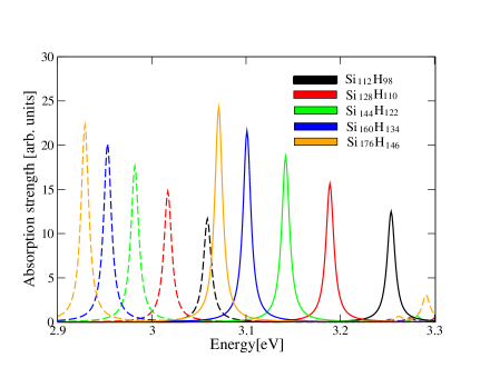
In 2, we show the absorption and luminescence spectra for the thinnest nanowire () with different lengths, from () to (). Similar to what we have previously observed in silicon quantum dots with increasing diameter,Wang2007 ; WangZLNF2007 we find here that both absorption and emission energies slightly red-shift with increasing wire length. Moreover, a sizable Stokes shift of around eV is discernible. Since excited state relaxation does not lead to a significant change in oscillator strengths, all considered nanostructures should exhibit significant luminescence intensity.
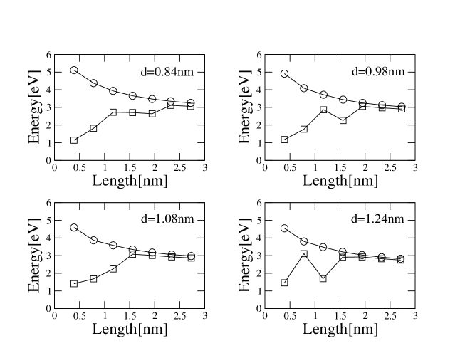
Next, we extracted the energies of the first allowed transition for SiNW with different diameters to investigate the size dependence of the optical gap (see 3). When the length of the Si nanostructures increases from 0.39 nm to 2.73 nm, the absorption energies will decrease monotonously from around 5 eV to around 3 eV. This is due to the decrease of quantum confinement effects. Concurrently, the emission energies show an overall increase (although with some fluctuations for most cases) from 1 eV to around 3 eV, and then follow the trend of the absorption energies. This general behaviour has also been found in similar studies on the size dependence of the optical gap in spherical Si quantum dots.Wang2007 ; WangZLNF2007 Quantum confinement effects are also observed in the radial dimension. Considering a fixed length of , the optical gap decreases from 3.66 eV for the thinnest diameter () to 3.21 eV for .
In order to understand the transition from quantum dots to wires more deeply, we analyze the geometrical distortions arising from the excited state relaxation. In small quantum dots, one Si-Si bond is extremely stretched up to 2.70 Å.WangZLNF2007 Depending on the actual structure, the location of this bond can be either in the center of the cluster or at its surface. When the rods are long enough, the geometry distortions are small and more homogenously distributed over all bonds. For the thinnest nanostructures (), the distortions locate at one Si-Si bond in the center of the structures for lengths less than 1.95 nm and delocalize beyond this value, owing to the confinement provided by the rigid surrounding layer.WangZLNF2007 For a diameter of 1.08 nm, geometry changes are observed for one Si-Si bond at the surface of the structures up to a length of 1.17 nm (). The situation for the other two cases ( and ) is more involved. For the wire with , distortions are found primarily for a Si-Si bond at the center of the quantum dots below 0.78 nm (). The distortion is then delocalized for the cluster at 1.17 nm, which corresponds to the peak in the emission energy curve in 3. It should be mentioned here that our simulation protocol locates the local minimum closest to the the Frank-Condon point, i.e. the initial structure after light absorption. It cannot be ruled out that the global minimum of the potential energy surface is again of localized nature. Whether luminescence occurs also from this state will crucially depend on the excited state lifetime and the kinetic energy of the ions after absorption. Excited state molecular dynamics simulations could shed light on this interesting question, which is however outside the scope of this study.
Turning back to the results, a surface Si-Si bond is found to be elongated for the cluster at 1.56 nm and thereafter all distortions have a delocalized character for longer structures. A similar case are the wires with , where a delocalized distortion appears for (), and a localized distortion for ().
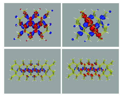
Additional information on the electronic structure can be extracted from the KS molecular orbitals that are involved in the light absorption and emission. Note-2 We take the rods () and () with diameter as examples. In both systems, the excited state wavefunction is dominated by a single-particle transitions from the highest occupied molecular orbital (HOMO) to the lowest unoccupied molecular orbital (LUMO). In 4, these orbitals are depicted for the optimized geometries in and . We find for the ground state minimum of both structures that the HOMO distributes mainly along the central zone of the wire, while the LUMO is located on the surface. The molecular orbitals at the excited state minimum conformation are quite different for the two structures under investigation. The shorter structure, , exhibits a LUMO concentrated at the center of the cluster that gives rise to a repulsive force. The significant Si-Si bond stretch in combination with the resulting sizable Stokes shift is completely in line with the self-trapped exciton model of Allan, Delerue, and Lannoo.allan1996nls ; Note-3 In contrast, the LUMO of the longer rod, , distributes more or less homogenously along the structure, indicating a delocalized exciton and geometry distortion.
IV Concluding Remarks
In conclusion, we simulated the absorption and emission spectra of SiNW with different diameters. The evolution of the optical properties from small quantum dots to nanowires with large aspect ratio has been investigated. While short nanorods with lengths below 2 nm show localized excitations and the formation of self-trapped excitons, excited state relaxation has little effect on longer structures which exhibit delocalized excited states. Notwithstanding these general trends, silicon nanostructures with similar extensions can exhibit quite different localization characteristics conjoined with largely differing emission profiles. This fact may partially explain the reported spread of photoluminescence energies wilcoxon1999oae and calls for atomistic simulations of these systems which take this strong conformation dependence into account.
V acknowledgement
Yong Wang thanks Dr. Xian Wang and Dr. Binghai Yan for useful discussions and MOST (No. 2006CB933000) of China for financial support.
References
- (1) Cui, Y.; Wei, Q. Q.; Park, H. K.; Liber, C. M. Science 2001, 293, 1289.
- (2) Cui, Y.; Lieber, C. M. Science 2001, 291, 851.
- (3) Gudiksen, M. S.; Lauhon, L. J.; Wang, J.; Smith, D. C.; Lieber, C. M. Nature 2002, 415, 617.
- (4) Duan, X. F.; Huang, Y.; Agarwal, R.; Lieber, C. M. Nature 2003, 421, 241.
- (5) Ma, D. D. D.; Lee, C. S.; Au, F. C. K.; Tong, S. Y.; Lee, S. T. Science 2003, 299, 1874.
- (6) Zhao, X. Y.; Wei, C. M.; Yang, L.; Chou, M. Y. Phys. Rev. Lett. 2004, 92, 236805.
- (7) Zhang, R. Q.; Lifshitz, Y.; Ma, D. D. D.; Zhao, Y. L.; Frauenheim, T.; Lee, S. T.; Tong, S. J. Chem. Phys. 2005, 123, 144703.
- (8) Ponomareva, I.; Menon, M.; Srivastava, D.; Andriotis, A. N. Phys. Rev. Lett. 2005, 95, 265502.
- (9) Yan, B. H.; Zhou, G.; Duan, W. H.; Wu, J.; Gu, B.-L. Appl. Phys. Lett. 2006, 89, 023104.
- (10) Bruno, M.; Palummo, M.; Marini, A.; Del Sole, R.; Ossicini, S. Phys. Rev. Lett. 2007, 98, 036807.
- (11) Aradi, B.; Ramos, L. E.; Deák, P.; Kölher, T.; Bechstedt, F.; Zhang, R. Q.; Th., F. Phys. Rev. B 2007, 76, 113303.
- (12) Rurali, R.; Aradi, B.; Frauenheim, T.; Gali, A. Phys. Rev. B 2007, 76, 113303.
- (13) Wolkin, M. V.; Jorne, J.; Fauchet, P. M. Phys. Rev. Lett. 1999, 82, 197.
- (14) Yu, D. P.; Bai, Z. G.; Wang, J. J.; Zou, Y. H.; Qian, W.; Fu, J. S.; Zhang, H. Z.; Ding, Y.; Xiong, G. C.; You, L. P.; Xu, J.; Feng, S. Q. Phys. Rev. B 1999, 59, R2498.
- (15) Li, C. P.; Sun, X. H.; Wong, N. B.; Lee, C. S.; Lee, S. T.; Teo, B. K. Chem. Phys. Lett. 2002, 365, 22.
- (16) Lyons, D. M.; Ryan, K. M.; Morris, M. A.; Holmes, J. D. Nano Lett. 2002, 2, 811.
- (17) Guichard, A. R.; Barsic, D. N.; Sharma, S.; Kamins, T. I.; Brongersma, M. L. Nano Lett. 2006, 6, 2140.
- (18) Niehaus, T. A.; Suhai, S.; Della Sala, F.; Lugli, P.; Elstner, M.; Seifert, G.; Frauenheim, T. Phys. Rev. B 2001, 6308, 085108.
- (19) Niehaus, T. A. J. Mol. Struct.: THEOCHEM, accepted for publication. 2009, .
- (20) Wang, X.; Zhang, R. Q.; Niehaus, T. A.; Frauenheim, T.; Lee, S. T. J. Phys. Chem. C 2007, 111, 12588.
- (21) Wang, X.; Zhang, R. Q.; Lee, S. T.; Niehaus, T. A.; Frauenheim, T. Appl. Phys. Lett. 2007, 90, 123116.
- (22) Li, Q.; Zhang, R. Q.; Niehaus, T. A.; Frauenheim, T.; Lee, S. T. Appl. Phys. Lett. 2007, 91, 043106.
- (23) Wang, X.; Zhang, R. Q.; Lee, S. T.; Frauenheim, T.; Niehaus, T. A. Appl. Phys. Lett. 2008, 93, 243120.
- (24) Li, Q. S.; Zhang, R. Q.; Lee, S. T.; Niehaus, T. A.; Frauenheim, T. Appl. Phys. Lett. 2008, 92, 053107.
- (25) Li, Q. S.; Zhang, R. Q.; Lee, S. T.; Niehaus, T. A.; Frauenheim, T. J. Chem. Phys. 2008, 128, 244714.
- (26) Li, Q. S.; Zhang, R. Q.; Niehaus, T. A.; Frauenheim, T.; Lee, S. T. J. Chem. Theo. Comp. 2007, 3, 1518.
- (27) Féher, F. Molekülspektroskopische Untersuchungen auf dem Gebiet der Silane und der heterocyclischen Sulfane; Westdeutscher Verlag: 1977.
- (28) Zdetsis, A. D. Rev. Adv. Mater. Sci. 2006, 11, 56.
- (29) Izmaylov, A.; Scuseria, G. J. Chem. Phys. 2008, 129, 34101.
- (30) Botti, S.; Schindlmayr, A.; Del Sole, R.; Reining, L. Rep. Prog. Phys. 2007, 70, 357.
- (31) Onida, G.; Reining, L.; Rubio, A. Rev. Mod. Phys. 2002, 74, 601.
- (32) Ramos, L. E.; Paier, J.; Kresse, G.; Bechstedt, F. Phys. Rev. B 2008, 78, 195423.
- (33) Elstner, M.; Porezag, D.; Jungnickel, G.; Elsner, J.; Haugk, M.; Frauenheim, T.; Suhai, S.; Seifert, G. Phys. Rev. B 1998, 58, 7260.
- (34) Heringer, D.; Niehaus, T. A.; Wanko, M.; Frauenheim, T. J. Comp. Chem. 2007, 28, 2589.
- (35) The respective DFTB integral tables are available as set pbc-0-2 from www.dftb.org.
- (36) Casida, M. E. Recent Advances in Density Functional Methods, Part I. In ; Chong, D., Ed.; World Scientific: 1995; Chapter Time-dependent Density Functional Response Theory for Molecules, pages 155.
- (37) Based on the eigenvectors of Eq. (1), it is possible to perform a qualitative decomposition of the excited state wavefunction in terms of singly excited Kohn-Sham determinants. Please see Ref.Casida1995 for details.
- (38) Allan, G.; Delerue, C.; Lannoo, M. Phys. Rev. Lett. 1996, 76, 2961.
- (39) For a recent review on excitons in nanoscale systems see also Scholes, G.D.; Rumbles, G. Nature Mat. 2006, 5, 683.
- (40) Wilcoxon, J. P.; Samara, G. A.; Provencio, P. N. Phys. Rev. B 1999, 60, 2704.