Surface reconstruction and energy gap of superconducting V3Si(001)
Abstract
A yet unknown surface reconstruction of V3Si(001), which is most likely induced by carbon, is used to investigate the quasi-particle energy gap at the atomic scale by a cryogenic scanning tunneling microscope. The width of the gap was virtually not altered at and close to carbon impurities, nor did it change at different sites of the reconstructed surface lattice. A remarkable modification of the spectroscopic signature of the gap was induced, however, upon moving the tip of the microscope into controlled contact with the superconductor. Spectroscopy of the resulting normal-metal – superconductor junction indicated the presence of Andreev reflections.
pacs:
68.35.bd, 68.37.Ef, 74.70.Ad, 74.45.cI Introduction
Superconductivity is one of the most vividly investigated research fields in solid state physics. In particular, spectroscopy of the energy gap of the quasi-particle density of states (DOS) has attracted considerable interest. Modifications of the energy gap by local impurities or by passing high currents through superconducting junctions have been recently studied. suhl ; gorkov ; woolf ; zittartz ; ali ; anderson ; jth_87 ; ehu_01 ; suc_01 ; spa_03 ; scheer ; cuevas ; post ; post_2 ; tinkhambook Effects of impurities on the energy gap suhl ; gorkov ; woolf ; zittartz ; ali ; anderson ; jth_87 ; ehu_01 ; suc_01 ; spa_03 provided valuable information about the interplay between superconductivity and magnetism or about the Cooper-pairing mechanism in unconventional superconductors, while high currents through superconducting contacts were used to unravel the number and transmission probability of transport channels via the occurrence of Andreev reflections. scheer ; cuevas ; post ; post_2 ; tinkhambook Until now such experiments have been restricted to conventional elemental superconductors with critical temperatures or to unconventional cuprate-based superconductors. ofi_07
In this article we present results of a combined scanning tunneling microscopy (STM) and spectroscopy (STS) study of the superconducting compound V3Si(001), which exhibits a yet unknown surface reconstruction. Auger electron spectroscopy (AES) reveals that this reconstruction is most likely induced by the presence of carbon. This surface is an ideal system to study possible local variations of the quasi-particle energy gap since it provides, owing to the reconstruction, carbon impurities and a spatially inhomogeneous geometry. Apart from these favorable properties, STM investigations of this surface are extremely scarce. Except for two investigations of the magnetic flux lines sosolik and Josephson tunneling nbe_08 on unreconstructed V3Si(001) using STM and STS, to our knowledge no additional STM and STS data are available for this surface. By combining a structural analysis using STM and an investigation of electronic properties with STS we found that the width of the energy gap is virtually independent of the position on the surface, while the symmetry of the gap is affected. We further investigated the current dependence on the tip-surface distance, from which we extracted the local apparent barrier height and the transition from tunneling to contact. At contact, spectra of the quasi-particle energy gap exhibited pronounced modifications compared to spectra acquired in the tunneling regime. These modifications are discussed in terms of Andreev reflections.
We used V3Si, which belongs to the class of A3B binary intermetallic compounds or, shortly, A15 materials. V3Si exhibits the -tungsten structure muller and is a type-II superconductor with a critical temperature of 17 K. hardy ; vonsovsky It has interesting electronic properties clogston ; morin ; williams such as a strong temperature dependence of the magnetic and electronic susceptibility and a large specific heat. Furthermore, V3Si undergoes a structural cubic-to-tetragonal phase transition at a temperature of 21.3 K, which exhibits characteristics of a thermo-elastic martensitic phase transition. paduani The concomitant change of lattice parameters is below the detection limit of STM. testardi We further notice that the occurrence of structural domain walls, which is attended by the martensitic transition is not related with the observed surface reconstruction, since the reconstruction is present already at room temperature.
The (001) surface of V3Si has attracted particular attention because of the hexagonal-to-square transformation of its vortex lattice structure yet1 ; kogan ; sosolik ; sonier ; yethiraj and the occurrence of surface reconstructions. aono ; zajac The energy gap has been determined by a variety of spatially averaging techniques nefyodov ; levinstein ; hauser ; schumaun ; moore ; bangert ; tanner ; hackl ; reinert yielding two distinct values of the zero-temperature energy gap either in the range from to or in the range from to . The existence of these two distinct values of has so far been explained by BCS theory in terms of overlapping bands.nefyodov ; suhlbcs ; moskalenko The first range of energy gaps is in good agreement with the value predicted by single-band s-wave BCS theory (). bcs
II Experiment
Measurements were performed with scanning tunneling microscopes operated in ultrahigh vacuum with a base pressure of and optimized for low temperatures of and for room temperature. Chemically etched tungsten tips were further prepared in vacuo by annealing and argon ion bombardment, while gold tips were cut at ambient conditions and used for the experiment without further treatment. The V3Si(001) surface of a polished single crystal was prepared by argon ion bombardment with ion energies between and and subsequent annealing at temperatures between and . Temperature readings from the pyrometer used in the experiments have an uncertainty margin of . All STM images were acquired in the constant-current mode with the voltage applied to the sample. STS measurements were performed in the constant-height mode. Spectra of the differential conductance () were acquired by superimposing a sinusoidal voltage signal (root-mean-square amplitude , frequency ) onto the tunneling voltage and by measuring the current response with a lock-in amplifier. For AES a cylindrical mirror analyser was used.
III Results and discussion
III.1 Characterization of reconstructed V3Si(001)
Depending on the preparation parameters, reconstructed or unreconstructed surfaces of V3Si(001) have been reported previously by Zajac et al. zajac They found by low-energy electron diffraction and AES that annealing of V3Si(001) at temperatures exceeding leads to a reconstruction, while the substrate surface is obtained for annealing temperatures lower than .
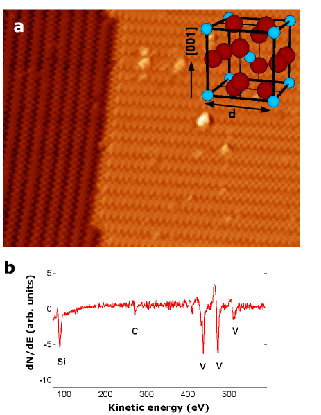
Figure 1(a) shows a room-temperature STM image of a V3Si(001) surface obtained using the preparation procedure introduced in the experimental section. The reconstruction observed here does not match the previously observed (2 1) or (1 1) meshes.
Terraces which exhibit parallel lines are observed. The corrugation of these lines is and almost independent of the voltages applied in the experiments (). The distance between two adjacent lines is (1.8 0.1) nm, which is approximately four times the lattice constant of V3Si, 0.47 nm. The lines on adjacent terraces are either parallel [not shown in Fig. 1(a)] or orthogonal with respect to each other. The step height between adjacent terraces with orthogonal orientation of the lines is , which corresponds to half a lattice constant of V3Si. Step heights between adjacent terraces with a parallel orientation of the lines are , which is similar to the V3Si lattice constant. Based on these observations we can tentatively identify the origin of the lines. To this end we refer to the inset of Fig. 1(a), which depicts a model of the V3Si lattice structure. Small filled spheres represent silicon atoms whereas large filled spheres represent vanadium atoms. The lattice constant is identical with the spacing of the silicon sublattice. On an unreconstructed V3Si(001) surface, vanadium atoms would form lines on the surface of a single crystal. According to this structural model, adjacent terraces with a step height of half a lattice constant exhibit lines of vanadium atoms, which are oriented perpendicular to each other. Analogously, terraces separated by one lattice constant show vanadium atom lines with the same orientation. This behavior matches our experimental observation and suggests that the lines originate from vanadium atoms. The mutual distance of the vanadium lines of , however, does not match the separation expected for the clean crystal.
To obtain more information about the reconstructed surface we used AES, which enables access to the chemical composition of the surface within the 5 top-most atomic layers depending on the material. chang An Auger spectrum of the reconstructed V3Si surface is shown in Fig. 1(b). In addition to spectroscopic signatures originating from vanadium (439 eV, 475 eV, 512 eV) and silicon (92 eV), a contribution from carbon (274 eV) is observed. Following the quantitative analysis of Auger spectra exposed in Ref. auger, , which takes into account the energy-dependent transmission function of the electron analyzer and the element-specific Auger sensitivity factors, the probed sample volume contains 8 % with respect to the total amount of detected elements. Taking into account the inelastic mean free path of carbon Auger electrons, we estimated that substrate layers within three to four lattice constants contribute significantly to the signal, so that the amount of carbon of 8 % gives the relative carbon concentration close to the surface. After excluding several other carbon sources such as the argon gas used for ion bombardment, the sample holder and the experimental setup, we surmise that carbon segregates from the bulk to the surface. Similar carbon-induced reconstruction like the one reported here have been reported for Si(001) and W(110). derycke ; yu ; tejeda ; bode In the latter case, carbon atoms arrange in a zigzag pattern, which is similar to our observations.
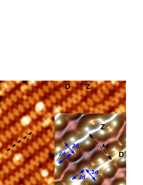
Figure 2 shows an STM image of a reconstructed surface area at 7.3 K in more detail. Two types of lines can be observed. The first type of lines shows circular protrusions which are arranged in a zigzag (Z) pattern on both sides of the line (dashed line). The same protrusions occur on opposite sites of the second type of lines and form a dimer (D) arrangement. We ascribe these protrusions to carbon atoms, which are arranged on opposite sites of the vanadium lines. The dimer and zigzag lines do not appear in an alternating pattern. We observed, however, that a carbon atom of a dimer line always faces a carbon atom of an adjacent line along a perpendicular direction with respect to the vanadium lines. This behavior may indicate an attractive interaction between the atoms. Some impurities are observed, which appear as bright protrusions. The inset of Fig. 2 shows a close-up view of a dimer and a zigzag line. The distance between two carbon atoms in a dimer line (solid arrows in the inset of Fig. 2) is (0.9 0.1) nm, which is approximately two times the lattice constant of V3Si. The same distance is obtained for zigzag lines if the carbon atoms on one side of a zigzag line are shifted by along this line. Thus, a zigzag line can be obtained by shifting the carbon atoms on one side of a dimer line by the lattice constant. The fact that two carbon atoms have a distance of roughly twice the lattice constant indicates that carbon atoms occupy every second lattice site of the silicon sublattice. Taking into account the martensitic transition of V3Si, the question may arise whether structural domain walls may be the origin of the reconstruction. However, the same reconstruction was observed at room temperature [Fig. 1(a)] and we conclude that the martensitic transition is not related with the observed surface reconstruction.
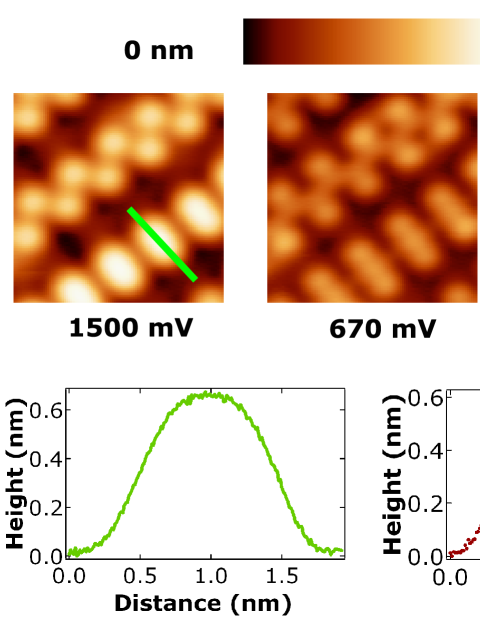
STM images of the same reconstructed surface area at several different tunneling voltages are shown in Fig. 3. Tip changes in between the acquisition of the different images can be excluded since all images were taken successively within 3 min. Furthermore, sudden changes in the tunneling current, which may indicate tip changes, were not observed. The vanadium lines become pronounced at small voltages ( 100 mV), which is indicated by dashed black lines, whereas they are hardly observed at high positive and negative voltages. This may indicate a one-dimensional state at low energies around the Fermi energy, which is located on the lines. Two findings lend support to this idea. First, a one-dimensional state is in agreement with an electronic model for the DOS of V3Si. clogston1 ; wegner ; labbe This model assigns quasi-one-dimensional character to the vanadium electrons, which gives rise to sharp peaks in the DOS close to the Fermi energy. First-principles calculations of the bulk band structure mattheiss ; mattheiss_2 ; klein ; pui ; mattheiss_3 ; bisi also exhibit an extremely narrow peak in the DOS right below the Fermi energy, which is mainly due to vanadium electrons. We note, however, that the calculations consider the bulk electronic structure, which may be modified at the surface. As a second indication favoring the presence of a one-dimensional state we mention the observation and calculation of a quasi-one-dimensional state on Fe(100) with segregated carbon. gpa_06 ; gtr_06 Similar to our observations carbon atoms form zigzag chains on Fe(100) and laterally confine Fe states, which gives rise to formation of a Fe surface state band with one-dimensional character near the Fermi level.
At small positive voltages (100 mV) the dimers in the dimer lines can clearly be distinguished as two atoms whereas at high negative and positive voltages ( 1500 mV) only a smeared shape can be seen. Two line scans on a dimer line are shown in Fig. 3, which were taken at positions indicated by the solid and dotted line, respectively. At 100 mV (right line scan in Fig. 3), the line and the two carbon atoms can be clearly distinguished (black arrows), while at 1500 mV (left line scan in Fig. 3), only a smeared shape can be seen. This loss of resolution can be understood on general grounds. Assuming a constant electronic structure of the STM tip, the tunneling current is an integral over the sample local density of states multiplied by a barrier transmission factor. The higher the tunneling voltage, the larger is the number of states contributing to the tunneling current. As a consequence, the localized one-dimensional state is dominated by other states. Only imaging at low voltages (here at 100 mV) gives rise to the sharp and localized lines along the dashed lines in Fig. 3. Further, some protrusions between the lines are observed (with a mutual distance of ), which become more pronounced at negative voltages. These protrusions are assigned to silicon atoms.
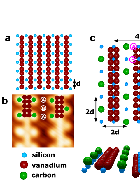
According to these experimental findings concerning the chemical composition ( 8 % carbon), the topographic (mutual atom distances), and electronic properties (chains of vanadium atoms) of the investigated surface as outlined above, a structural model for the reconstructed surface areas is proposed in the following. The top-most unreconstructed V3Si(001) surface layer is shown in Fig. 4(a), where silicon and vanadium atoms are indicated by small and large spheres, respectively. Two neighboring vanadium lines of the top-most unreconstructed surface layer are proposed to form double rows [Fig. 4(c)]. Every other double row of vanadium moves below the silicon sublattice into the second crystal layer whereas the other vanadium double rows move slightly above the silicon sublattice. The distance between the top double rows is , matching the distance extracted from STM images. Carbon atoms are attached to the lines on top of some silicon atoms. Dimer lines as well as zigzag lines are formed in this way. The distance between two carbon atoms in a dimer line in this model is . This distance and also the corresponding distance in the zigzag lines is in agreement with the measurements (compare with the inset in Fig. 2). Figure 4(b) shows an STM image of a reconstructed surface area where carbon and vanadium atoms are depicted by spheres. Silicon atoms denoted A and B in Fig. 4(c) are embedded in different environments regarding the neighbor atoms. They are either neighbored by two carbon atoms and four underlying silicon atoms (position A) or by just four silicon atoms (position B). Only the latter silicon atoms can be observed in the reconstructed surface areas as protrusions between the lines [position B in Fig. 4(b)].
III.2 Superconducting energy gap
V3Si is a conventional intermediate-coupling superconductor. vonsovsky ; poole The DOS of the quasi-particles for intermediate-coupling is described according to Eliashberg.eliashberg For simplicity, in this work we assume the energy gap to be solely temperature-dependent, , such that the quasi-particle DOS can be written as the lifetime-broadened BCS expression for the quasi-particle DOS, , given by dynes ; alexandrov
| (1) |
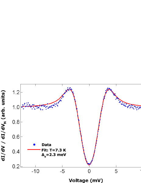
where is the DOS of normal conducting electrons and is a lifetime parameter. We consider a broadening due to the temperature as well as a broadening due to the lock-in amplifier by convoluting with the temperature-broadening function as well as with the instrumental broadening function of the lock-in amplifier.klein_inst ; kroeger We assume the lifetime-broadening to be of the order of 0.1 meV dynes whereas the temperature-broadening is around 2.2 meV full width at half maximum (FWHM) at 7.3 K. kroeger Therefore, for our fits the lifetime parameter is set to a small value such that increasing by a factor does not change our results. Thus only the temperature and the energy gap are used as fit parameters. The spectra close to the Fermi energy are normalized to the differential conductance at 12 mV (), which is well outside the energy gap. The current at 12 mV was set to values between 0.5 nA and 1 nA. A typical fit to the data (dots) is shown as a solid line in Fig. 5. Best fits are obtained for temperatures between 7.2 K and 7.8 K, which are in good agreement with the temperature of the experiment. Our fits yield energy gaps within this temperature range. According to BCS theory, this corresponds to a maximal energy gap at 0 K of 0.20) meV with 17 K. These results are in reasonable accordance with previous measurements. nefyodov ; levinstein ; hauser ; schumaun ; moore ; bangert ; tanner ; reinert However, comparing our results with most recent measurements nefyodov ; reinert we find slightly lower gap widths, which may be related to structural changes at the surface due to the carbon-induced reconstruction.
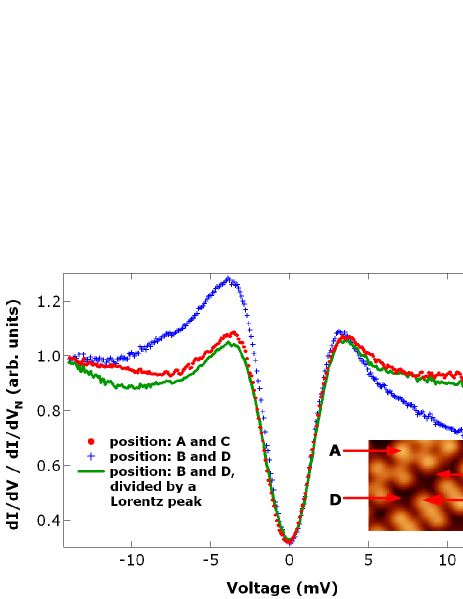
To probe a local effect on we acquired spectra at different positions of the reconstructed surface, which are defined in the inset of Fig. 6. Normalized spectra of were taken either on atoms of the dimer or zigzag pattern (positions A and C) or between the lines (positions B and D). Differences between spectra taken at positions A and C and taken at positions B and D are hardly detectable, so that mainly two different curves can be observed, which are shown in Fig. 6. Spectra of taken at positions A and C (dots) are symmetric with respect to zero voltage whereas those at positions B and D (crosses) are asymmetric. For small negative sample voltages, the differential conductance is higher at positions B and D than at positions A and C. This behavior may be due to the DOS of normal conducting electrons , which is different for positions A and C (on the lines) and positions B and D (between the lines). Typically, is treated as constant, which leads to a symmetric around the Fermi energy. Since the atomic environment of atoms at different positions of the reconstructed surface areas is different in the present case, it is likely that varies locally, too. If has asymmetric features within a small energy range around the Fermi energy, the energy gap can be asymmetric. As it can be seen from Eq. (1), the influence of can be cancelled by dividing by . An angle-resolved photoemission study of V3Si(001) performed at room temperature revealed the existence of a remarkably sharp peak close to the Fermi level and in the center of the surface Brillouin zone. aono This contribution to the density of states of normal conducting electrons may give rise to the observed asymmetry of the measured energy gap in spectra of . In a first approximation, we divided the asymmetric spectrum by a Lorentzian (maximum at 5 meV and FWHM of 29 meV) in order to remove the asymmetry. The result is depicted in Fig. 6 by the solid curve. The asymmetric behavior is nearly compensated and the solid curve fits well with the symmetric spectrum.
III.3 Contact spectroscopy
To perform contact spectroscopy the tip had to be moved controllably into contact with the V3Si(001) surface. For this purpose we proceeded as reported in Ref. lli_05, and monitored the conductance (, : current, : voltage) over a range of tip displacements comprising tunneling and contact regimes. Unlike on noble metal surfaces lli_05 ; nne07a ; jkr_07 the contact to V3Si(001) is not always signaled by a jump of the conductance. We also observed a continuous transition from the tunneling to the contact regime. Contact conductances are defined according to the procedure exposed in Ref. jkr_08, . Contact conductances defined in this way scatter between and where denotes the quantum of conductance (h: Planck’s constant). Once the contact regime is reached the tip could be moved further into the surface increasing the conductance to up to without destroying the sample surface and tip integrity. From conductance curves acquired in the tunneling regime we inferred the apparent barrier height within a one-dimensional model of the tunneling junction. simmons ; lang ; olesen The apparent barrier height () was determined by using a tungsten tip and also by using a gold tip. From our contact measurements we obtained (4.600.5) eV and (4.190.2) eV. In the simplest case, the work function of the sample (denoted ) is given by . Taking into account the work functions for polycrystalline specimen of W, , and Au, , from Ref. michaelson, , the work function of V3Si is . Our result is in agreement with previous measurements of the work function of V3Si, which yield 4.4 eV for single-crystalline V3Si(001) aono and 4.6 eV for a polycrystalline sample. heiniger
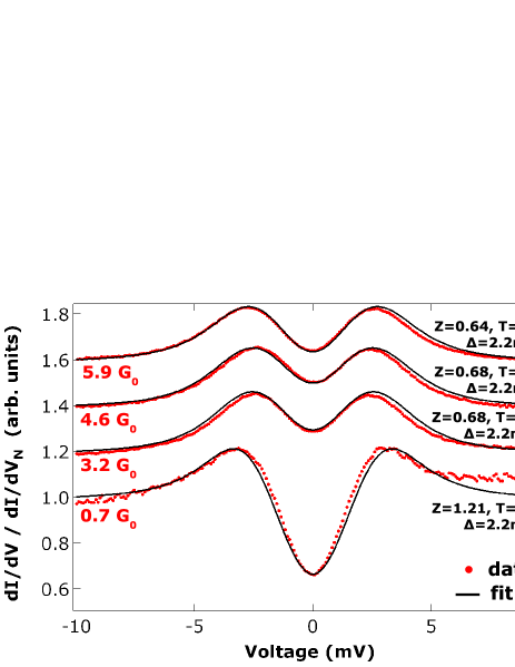
For contact spectroscopy we proceeded as follows. We first acquired a conductance-versus-displacement curve in order to find the contact regime. We then set a junction conductance corresponding to tip-surface contact and performed spectroscopy of as previously reported in Refs. nne07a, ; nne_08, ; nne_09, . Typical results for various junction conductances are shown in Fig. 7. The spectra are normalized to the conductance value at -14 mV and are shifted vertically with respect to each other. The energy gap in the spectra becomes less pronounced at higher conductances of the junction, i. e., the indentation of the curves between the condensation peaks becomes shallower upon increasing the junction conductance. To model this behavior we first tried to fit the BCS density of states with an increased effective temperature to the data. Several contact experiments have been reported where local heating of the contact junction due to a high current density plays a significant role. nne07b ; gsc_08 However, increasing the effective temperature in the BCS density of states, Eq. (1), decreases the condensation peaks, which is not observed in our data.
The apparent change of the superconducting energy gap with increasing junction conductance may be explained by taking Andreev reflections into account. benistant ; soulen ; strijkers ; andreev To fit our data, we use a theoretical approach to Andreev reflections at an interface between a normal-metal and a superconductor reported by Blonder et al. blonder These authors introduced a -function potential barrier of strength to describe the normal-metal – superconductor interface. For a large barrier strength () calculated spectra agree with data acquired in the tunneling regime (Fig. 5). We used the energy gap, , the temperature, , and the dimensionless barrier strength, , as fitting parameters. Fits for the spectra at different conductances are shown in Fig. 7 by solid lines. The quality of the fits is quite remarkable indicating that Andreev reflections play a role in our contact spectroscopy of the V3Si(001) energy gap.
IV Summary
STM of V3Si(001) reveals a surface reconstruction, which is most likely induced by carbon. Based on atomically resolved STM images and on the chemical composition of the surface as monitored by AES we suggest a structural model of this reconstruction. Spatially resolved spectroscopy revealed that the width of the energy gap does not depend on the surface site, while the symmetry of the gap is affected depending on the local environment. The spectroscopic signature of the energy gap changes in the contact regime. These modifications are compatible with Andreev reflections in the point contact between a normal metal tip and a superconductor.
We thank M. Ternes for discussions and the Deutsche Forschungsgemeinschaft for financial support through KR 2912 3-1.
References
- (1) B. T. Matthias, H. Suhl, and E. Corenzwit, Phys. Rev. Lett. 1, 92 (1958).
- (2) A. A. Abrikosov and L. P. Gorkov, Sov. Phys. JETP 12, 1243 (1960).
- (3) M. A. Woolf and F. Reif, Phys. Rev. 137, A557 (1965).
- (4) J. Zittartz, A. Bringer, and E. Müller-Hartmann, Solid State Commun. 10, 513 (1972).
- (5) A. Yazdani, B. A. Jones, C. P. Lutz, M. F. Crommie, and D. M. Eigler, Science 275, 1767 (1997).
- (6) P. W. Anderson, J. Phys. Chem. Solids 11, 26 (1959).
- (7) J. R. Thompson, D. K. Christen, S. T. Sekula, B. C. Sales, and L. A. Boatner, Phys. Rev. B36, 836 (1987).
- (8) E. W. Hudson, K. M. Lang, V. Madhavan, S. H. Pan, H. Eisaki, S. Uchida, and J. C. Davis, Nature 411, 920 (2001).
- (9) S. Uchida, Physica C 357, 25 (2001).
- (10) S. H. Pan, E. W. Hudson, K. M. Lang, H. Eisaki, S. Uchida, and J. C. Davis, Nature 403, 746 (2003).
- (11) E. Scheer, N. Agraït, J. C. Cuevas, A. Levy Yeyati, B. Ludoph, A. Martín-Rodero, G. Rubio Bollinger, J. M. van Ruitenbeek, and C. Urbina, Nature 394, 154 (1998).
- (12) J. C. Cuevas, A. Levy Yeyati, A. Martín-Rodero, G. R. Bollinger, C. Untiedt, and N. Agraït, Phys. Rev. Lett. 81, 2990 (1998).
- (13) N. van der Post, E. T. Peters, I. K. Yanson, and J. M. van Ruitenbeek, Phys. Rev. Lett. 73, 2611 (1994).
- (14) E. N. Bratus’, V. S. Shumeiko, and G. Wendin, Phys. Rev. Lett. 74, 2110 (1995).
- (15) M. Tinkham, Introduction to Superconductivity, (McGraw-Hill, Inc., New York, 1996).
- (16) Ø. Fischer, M. Kugler, I. Maggio-Aprile, C. Berthold, and C. Renner, Rev. Mod. Phys. 79, 353 (2007).
- (17) C. E. Sosolik, J. A. Stroscio, M. D. Stiles, E. W. Hudson, S. R. Blankenship, A. P. Fein, and R. J. Celotta, Phys. Rev. B68, 140503(R)(2003).
- (18) N. Bergeal, Y. Noat, T. Cren, Th. Proslier, V. Dubost, F. Debontridder, A. Zimmers, D. Roditchev, W. Sacks, and J. Marcus, Phys. Rev. B78, 140507(R) (2008).
- (19) J. Muller, Rep. Prog. Phys. 43, 641 (1980).
- (20) G. F. Hardy and J. K. Hulm, Phys. Rev. 5, 1004 (1954).
- (21) S. V. Vonsovsky, Yu. A. Izyumov, and E. Z. Kurmaev, Superconductivity of Transition Metals, (Springer-Verlag, Berlin, 1982).
- (22) A. M. Clogston, A. C. Gossard, V. Jaccarino, and Y. Yafet, Phys. Rev. Lett. 9, 262 (1962).
- (23) F. J. Morin and J. P. Maita, Phys. Rev. 129, 1115 (1963).
- (24) H. J. Williams and R. C. Sherwood, Bull. Am. Phys. Soc. 5, 430 (1960).
- (25) C. Paduania and C. A. Kuhnen, Eur. Phys. J. B 66, 353 (2008).
- (26) L. R. Testardi, Rev. Mod. Phys. 47, 637 (1975).
- (27) M. Yethiraj, D. K. Christen, D. McK. Paul, P. Miranovic, and J. R. Thompson, Phys. Rev. Lett. 82, 5112 (1999).
- (28) V. G. Kogan, P. Miranovic, Lj. Dobrosavljevic-Grujic, W. E. Pickett, and D. K. Christen, Phys. Rev. Lett. 79, 741 (1997).
- (29) J. E. Sonier, F. D. Callaghan, R. I. Miller, E. Boaknin, L. Taillefer, R. F. Kiefl, J. H. Brewer, K. F. Poon, and J. D. Brewer, Phys. Rev. Lett. 93, 017002 (2004).
- (30) M. Yethiraj, D. K. Christen, A. A. Gapud, D. McK.Paul, S. J. Crowe, C. D. Dewhurst, R. Cubitt, L. Porcar, and A. Gurevich, Phys. Rev. B72, 060504(R) (2005).
- (31) G. Zajac, J. Zak, and S. D. Bader, Phys. Rev. B27, 6649 (1983).
- (32) M. Aono, F. J. Himpsel, and D. E. Eastman, Solid State Commun. 39, 225 (1981).
- (33) Yu. A. Nefyodov, A. M. Shuvaev, and M. R. Trunin, Europhys. Lett. 72, 638 (2005).
- (34) H. J. Levinstein and J. E. Kunzler, Phys. Lett. 20, 581 (1966).
- (35) J. J. Hauser, D. D. Bacon, and W. H. Haemmerle, Phys. Rev. 151, 296 (1966).
- (36) J. Schumaun and D. Elefant, Phys. Status Solidi B 95, 91 (1979).
- (37) D. F. Moore, R. B. Zubeck, J. M. Rowell, and M. R. Beasley, Phys. Rev. B20, 2721 (1979).
- (38) W. Bangert, J. Geerk, and P. Schweiss, Phys. Rev. B31, 6066 (1985).
- (39) D. B. Tanner and A. J. Sievers, Phys. Rev. B8, 1978 (1973).
- (40) R. Hackl, R. Kaiser, and W. Gläser, Physica C 162-164, 431 (1989).
- (41) E. Reinert, G. Nicolay, S. Hüfner, U. Probst, and E. Bucher, J. Electron Spectrosc. Relat. Phenom. 114-116, 615 (2001).
- (42) H. Suhl, B. T. Matthias, and L. R. Walker, Phys. Rev. Lett. 3, 552 (1959).
- (43) V. Moskalenko, Fiz. Met. Metalloved. 8, 503 (1959).
- (44) J. Bardeen, L. N. Cooper, and J. R. Schrieffer, Phys. Rev. 108, 1175 (1957).
- (45) C. C. Chang, Surf. Sci. 25, 53 (1971).
- (46) L. E. Davis, N. C. MacDonald, P. W. Palmberg, G. E. Riach, and R. E. Weber, Handbook of Auger Spectroscopy, (Physical Electronics Industries).
- (47) V. Derycke, P. Soukiassian, A. Mayne, G. Dujardin, and J. Gautier, Phys. Rev. Lett. 81, 5868 (1998).
- (48) V. Yu. Aristov, P. Soukiassian, A. Catellani, R. DiFelice, and G. Galli, Phys. Rev. B69, 245326 (2004).
- (49) A. Tejeda, E. Wimmer, P. Soukiassian, D. Dunham, E. Rotenberg, J. D. Denlinger, and E. G. Michel, Phys. Rev. B75, 195315 (2007).
- (50) M. Bode, R. Pascal, and R. Wiesendanger, Surf. Sci. 344, 185 (1995).
- (51) A. M. Clogston and V. Jaccarino, Phys. Rev. 121, 1357 (1961).
- (52) M. Wegner, Rev. Mod. Phys. 36, 175 (1964).
- (53) J. Labbé and J. Friedel, J. Phys. Radium 27, 153 (1966).
- (54) L. F. Mattheiss, Phys. Rev. 138, A112 (1965).
- (55) L. F. Mattheiss, Phys. Rev. B12, 2161 (1975).
- (56) B. M. Klein, L. L. Boyer, D. A. Papaconstantopoulos, and L. F. Mattheiss, Phys. Rev. B18, 6411 (1978).
- (57) P. K. Lam and M. L. Cohen, Phys. Rev. B23, 6371 (1981).
- (58) L. F. Mattheiss and W. Weber, Phys. Rev. B25, 2248 (1982).
- (59) O. Bisi and L. W. Chiao, Phys. Rev. B25, 4943 (1982).
- (60) G. Panaccione, J. Fujii, I. Vobornik, G. Trimarchi, N. Binggeli, A. Goldoni, R. Larciprete, and G. Rossi, Phys. Rev. B73, 035431 (2006).
- (61) G. Trimarchi and N. Binggeli, Phys. Stat. Sol. B 243, 2105 (2006).
- (62) C. P. Poole, H. A. Farach, and R. J. Creswick, Superconductivity, (Academic Press, New York, 1995).
- (63) G. M. Eliashberg, Zh. Eksp. Teor. Fiz. 38, 966 (1960).
- (64) R. C. Dynes, V. Narayanamurti, and J. P. Garno, Phys. Rev. Lett. 41, 21, 1509 (1978).
- (65) A. S. Alexandrov, Theory of superconductivity - from weak to strong coupling, (Institute of Physics Publishing, Bristol, 2003)
- (66) J. Klein, A. Léger, M. Belin, D. Défourneau, and M. J. L. Sangster, Phys. Rev. B7, 2336 (1973).
- (67) J. Kröger, L. Limot, H. Jensen, R. Berndt, S. Crampin, and E. Pehlke, Prog. Surf. Sci. 80, 26 (2005).
- (68) L. Limot, J. Kröger, R. Berndt, A. Garcia-Lekue, and W. A. Hofer, Phys. Rev. Lett. 94, 126102 (2005).
- (69) N. Néel, J. Kröger, L. Limot, K. Palotas, W. A. Hofer, and R. Berndt, Phys. Rev. Lett. 98, 016801 (2007).
- (70) J. Kröger, H. Jensen, and R. Berndt, New J. Phys. 9, 153 (2007).
- (71) J. Kröger, N. Néel, and L. Limot, J. Phys.: Condens. Matter 20, 223001 (2008).
- (72) J. G. Simmons, J. Appl. Phys. 34, 1793 (1963).
- (73) N. D. Lang, Phys. Rev. B37, 10395 (1988).
- (74) L. Olesen, M. Brandbyge, M. R. Sørensen, K. W. Jacobsen, E. Lægsgaard, I. Stensgaard, and F. Besenbacher, Phys. Rev. Lett. 76, 1485 (1996).
- (75) H. B. Michaelson, J. Appl. Phys. 48, 4729 (1977).
- (76) F. Heiniger and L. Walldén, Phys. Status Solidi 5, 82 (1971).
- (77) N. Néel, J. Kröger, L. Limot, and R. Berndt, Nano Lett. 8, 1291 (2008).
- (78) N. Néel, J. Kröger, R. Berndt, and E. Pehlke, Phys. Rev. B78, 233402 (2008).
- (79) N. Néel, J. Kröger, L. Limot, T. Frederiksen, M. Brandbyge, and R. Berndt, Phys. Rev. Lett. 98, 065502 (2007).
- (80) G. Schulze, K. J. Franke, A. Gagliardi, G. Romano, C. S. Lin, A. L. Rosa, T. A. Niehaus, Th. Frauenheim, A. Di Carlo, A. Pecchia, and J. I. Pascual, Phys. Rev. Lett. 100, 136801 (2008).
- (81) P. A. M. Benistant, H. van Kempen, and P. Wyder, Phys. Rev. Lett. 51, 817 (1983).
- (82) R. J. Soulen Jr., J. M. Byers, M. S. Osofysky, B. Nadgorny, T. Ambrose, S. F. Cheng, P. R. Broussard, C. T. Tanaka, J. Nowak, J. S. Moodera, A. Barry, and J. M. D. Coey, Science 282, 85 (1998).
- (83) G. J. Strijkers, Y. Ji, F. Y. Yang, C. L. Chien, and J. M. Byers, Phys. Rev. B63, 104510 (2001).
- (84) A. F. Andreev, Zh. Eksp. Teor. Fiz. 46, 1823 (1964).
- (85) G. E. Blonder, M. Tinkham, and T. M. Klapwijk, Phys. Rev. B25, 4515 (1982).
- (86) Yu. V. Sharvin, Zh. Eksp. Teor. Fiz. 48, 984 (1965).