Fundamental mechanism underlying subwavelength optics of metamaterials: Charge oscillation-induced light emission and interference
Abstract
Interactions between light and conducting nanostructures can result in a variety of novel and fascinating phenomena. These properties may have wide applications, but their underlying mechanisms have not been completely understood. From calculations of surface charge density waves on conducting gratings and by comparing them with classical surface plasmons, we revealed a general yet concrete picture about coupling of light to free electron oscillation on structured conducting surfaces that can lead to oscillating subwavelength charge patterns (i.e., spoof surface plasmons but without the dispersion property of classical surface plasmons). New wavelets emitted from these light sources then destructively interfere to form evanescent waves. This principle, usually combined with other mechanisms (e.g. resonance), is mainly a geometrical effect that can be universally involved in light scattering from all periodic and nonperiodic structures containing free electrons, including perfect conductors. The spoof surface plasmon picture may provide clear guidelines for developing metamaterial-based nano-optical devices.
pacs:
42.25.Bs, 42.79.Dj, 73.20.Mf, 84.40.AzI Introduction
The various novel and unusual optical properties of conducting nanostructures, such as anomalous diffraction from metallic gratings, enhanced light transmission through subwavelength slits or holes, light polarizing through wire grid polarizers, surface-enhanced Raman scattering, negative refraction imaging, etc, have attracted tremendous attention in recent years.r1 ; r2 ; r3 ; WGP ; ZhangX To date the coupling of light with surface plasmons (SPs) have been widely adopted to explain these anomalous phenomena. However, the SP picture elaborated in numerous case studies in the literature actually corresponds to a very general concept about coupling of electromagnetic (EM) waves to free electron oscillation on conducting surfaces that can generate evanescent EM wave modes. This big picture is correct without doubt, but it is too general for one to obtain a clear and straightforward understanding of the essential underlying mechanism. Due to this uncertainty, the SP-like wave modes have been usually assumed to be similar to the classical SPs (CSPs) on planar metal surfaces,CSP but this assumption is obviously challenged by the fact that (nearly) perfectly conducting structures that do not support CSPs still have similar but stronger anomalous light scattering properties.Nanowire2 Conductors with positive permittivity do not support CSPs either, but they can also exhibit light transmission anomalies.Lezec1 ; PRA ; Sarrazin (Extraordinary transmission through gratings can even occur for acoustic waves,Ming which is completely irrelevant to SPs.) Because of these contradictions, the origin of anomalous light scattering from metallic nanostructures is still being argued (e.g. Refs. Lezec2, -NGarcia, ).
Using modern computing techniques one may numerically solve Maxwell’s equations for various complicated structures, but such computations have been largely focused on the EM fields. Surprisingly, the detailed mechanisms of free electron oscillation have been almost completely ignored in the literature although they are known to play the essential role in the SP picture. Very recently, we have briefly reported our computations of surface charge density waves (SCDWs) and the role they play in the process of enhanced light transmission through slit and hole arrays.PRA In this paper, we give a detailed and comprehensive illustration of the basic mechanism about light emission and interference from incident-wave-driven free electron oscillations, demonstrate that it is involved in light scattering from all periodic and nonperiodic conducting structures (including perfect conductors), and thus establish a simple, concrete and universal spoof SP picture. This picture may provide solid guidelines for designing nano-optical devices by directing people to concentrate on the geometrical parameters of conducting nanostructures so as to control the locations, strengths, and interference of the charge oscillation-induced light sources.
II charge oscillation-induced light emission and interference
To illustrate the main picture, we start from the well-known principle of Thomson scattering of x-rays by electrons,XrayBook in which the incident x rays (EM waves with wavelengths nm) force the electrons in atoms (not necessarily free electrons) to oscillate with the same frequency. According to the fact that accelerating charges radiate, the oscillating electrons then emit new wavelets, which form the scattered waves. In principle, this effect also exists in the long wavelength range (say m), where electrons still oscillate with the incident wave (giving rise to oscillating polarization of the atoms). However, since now is much larger than the atoms ( nm), the net charge density averaged on the wavelength scale is zero in the bulk. Net polarization-induced charges do exist on surfaces (or interfaces), but for non-conducting materials where electrons are bound to atoms and cannot move freely, the formation of net oscillating charges is very small even on rough surfaces.
A metal has free electrons, which move/oscillate easily on the surface in response to external EM waves and thus may emit new wavelets. But first note that a CSP corresponds to a surface-bound mode on the metal. If the oscillating charges emit light, how can the CSP be non-radiative? To clarify this ambiguity, let us see the Otto geometry in Fig. 1(a) as an example.CSP At a specific incident angle [greater than the critical angle of the prism-vacuum interface], the incident wave can excite a CSP, which is a sinusoidal SCDW on the metal surface with a wavevector
| (1) |
where is the permittivity of the metal and ( the incident wavelength in vacuum). Here must satisfy , where is the refractive index of the prism. Under this condition, the incident energy is largely transferred to the CSP, giving rise to a reflection dip, as can be proved by Fresnel theory.CSP
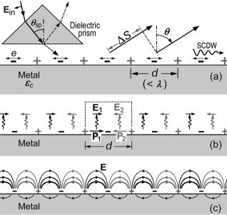
Note that CSPs can be activated only on metals with Re [and meanwhile Im being small].CSP The reason is that under this condition, the spatial period of the CSP satisfies
| (2) |
based on Eq. (1). Therefore, the CSP is a subwavelength charge pattern compared with the incident wavelength . Consider each period of the CSP in Fig. 1(a) as a scatter unit that emits new wavelets. Along any arbitrary direction , the wavelets emitted from two adjacent units have a path difference
| (3) |
i.e., the phase difference is less than . This means that the oblique wavelets can never be in phase. Thus, they tend to cancel each other out in the far fields. The wavelets along the vertical direction , however, are in phase (), but viewed from a single period of the sinusoidal SCDW [Fig. 1(b)], each wavelet consists of two sub-wavelets with opposite electric fields and that are also cancelled in the far fields. Therefore, all the emitted wavelets cannot escape the surface along any direction, so they form evanescent waves near the surface [Fig. 1(c)]. This gives a simple picture why a CSP corresponds to a surface-bound mode. The CSP can thus propagate outside the prism-covered region in Fig. 1(a) without radiation loss, and the propagation distance solely depends on the absorption of the metal (Ohmic loss). Here it is obvious that media with (for perfect conductors) or Re do not support CSPs as the wavevector in Eq. (1) cannot satisfy Eq. (2) under these conditions.
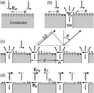
Now we consider in Fig. 2(a) a plane wave incident on a conducting surface without the prism. For normal incidence, the incident electric field drives free electrons on the surface to move homogenously. So there is no net charge, and the reflection obeys Fresnel equations.Born In Fig. 2(b), a slit (or hole) is added. Apparently, the electron movement now can be impeded near the slit corner. Here some electrons may move continuously to the vertical slit wall, but such movement corresponds to a deflection (acceleration) while the incident wave does not directly provide the necessary large driving force. So it is reasonable to assume that most of the moving electrons are stopped near one corner, while positive charges appear at the opposite corner because some electrons have moved away. This leads to the formation of an electric dipole at the slit opening. oscillates with the incident wave with a time factor ( the angular frequency of the incident wave), thus acting as a new light source emitting wavelets. Such a process is in fact a Thomson scattering process in the optical frequency range.
Next we apply this process to the one-dimensional (1D) periodic slit array in Fig. 2(c). For simplicity, we assume that the grating is semi-infinite so that there is no feedback from below. Similar to Fig. 2(b), now each slit becomes a light source, but along any oblique direction , the wavelets emitted from two adjacent sources have a path difference , where is the period of the slit array. For an incident wavelength , Eq. (3) is satisfied again. Then the oblique wavelets are cancelled out in the far fields (destructive interference, similar to the absence of x-ray diffraction at non-Bragg angles), i.e., they also form evanescent waves near the surface. (This principle can also explain the fact that no light diffraction occurs from single crystal lattice, where the lattice constants are much smaller than the wavelength although the electrons still oscillate with the incident wave.)
The charge pattern in Fig. 2(c) is similar to the CSP picture in Fig. 1, i.e., they are both subwavelength charge patterns (). However, there are two distinct differences. First, the CSP is a propagating wave with a specific wavevector determined by the metal’s permittivity in Eq. (1), while the charge pattern in Fig. 2(c) is a standing wave (but not sinusoidal) with the period always equal to the grating period . So the former is an intrinsic property of the metal (depending on ) while the latter is a geometrical effect that can occur for any incident wavelength and for any conducting materials containing free electrons [including perfect conductors and conductors with Re]. Second, as mentioned above, a CSP is a complete surface-bound mode. In contrast, the oscillating charge pattern in Fig. 2(c) is radiative along (). This can be seen from Fig. 2(d), where we have discarded the oblique evanescent wavelets and added the dipoles that are ignored in Fig. 2(c). In addition to the wavelet emitted from , also emits a wavelet along with a phase that is usually very close to that of the Fresnel reflected wave. So here we let include Fresnel reflection for convenience in discussions. Then the wavelet emitted from a period consists of two sub-wavelets and along with opposite directions (phases). But unlike Fig. 1(b), and generally have different strengths, so they cannot completely offset each other. This leads to a propagating backward wave. Therefore, the charge pattern illustrated in Figs. 2(c) and 2(d) is not a CSP, but one might call it a spoof SP due to its similarities to the true CSP in Fig. 1(a).Pendry ; Pendry2
From Fig. 2 it is not difficult to obtain a general picture about light scattering from structured (or rough) conducting surfaces (either periodic or nonperiodic). When light is incident on a non-planar conducting surface, it drives the free electrons to move, but the movement can be impeded by the rough parts (particularly sharp edges) of the surface to form inhomogeneous oscillating charges, which become new light sources to emit wavelets. It is the interference between these wavelets that may give rise to anomalous reflection or scattering. In the following, we will numerically prove this mechanism in the simple and well studied case of periodic 1D gratings using the rigorous coupled-wave analysis (RCWA) technique.RCWA1 ; RCWA2
III RCWA of 1D lattice
For monochromatic waves in a nonmagnetic medium (permeability ), the electric and magnetic fields are coupled by Maxwell’s equations (in c.g.s. units)
| (4) | |||||
| (5) |
where and is the effective permittivity. The effective permittivity of a conductor can be expressed as , where is the regular permittivity and is the conductivity.Born For perfect conductors, so that Im (which can also be derived from the Drude model of electrical conduction). The divergence of Eq. (5) gives , or
| (6) |
where is the bulk charge density (including both free and polarization-induced charges). In a modulated medium with varying , , which generally leads to inhomogeneous charge densities according to Eq. (6). Mathematically, is discontinuous across a sharp interface (i.e., ), so one has to use the surface charge density to describe the charge distribution on the interface, where is the jump of the perpendicular electric field component across the interface. As an exception, TE-polarization in a 1D structure satisfies since , so here we ignore it.PRA
From Eqs. (4) and (5) one can obtain a second-order differential equation , of which the Fourier transformation form for the 1D lattice in Fig. 3 is
| (7) |
based on the Fourier expansions and , where ( being integers), , , and is the forward wavevector. Eq. (7) can be numerically solved by RCWA. Here we briefly mention its main principles.
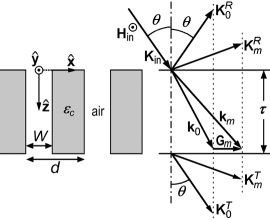
In Fig. 3, the incident wave is with . The forward wavevector can be written as with , where is to be determined by the eigenequation. Then the internal diffracted wavevectors have the form with . Each diffraction order corresponds to two diffracted waves and above and below the grating, respectively. Based on the conservation of the tangential wavevector components, we have
| (10) |
Here note that when , the corresponding external waves become evanescent waves along . In particular, for normal incidence () and , all the external waves except for are evanescent, . This is the mathematical description of the evanescent EM waves of the spoof SP described in Fig. 2.
For TM polarization, all the magnetic fields are parallel to . If we retain diffraction orders (, , , ), Eq. (7) can be written as a matrix eigenequation. From this eigenequation and the boundary conditions (continuity of the tangential electric and magnetic fields) at the two surfaces , one obtains sets of eigenvalues and eigenmodes (, , , and , , , ) inside the grating and two sets of external fields and (see Refs. RCWA1, and RCWA2, for details). Then the zero-order reflectivity and transmissivity are and , respectively. Meanwhile, the electric fields , and (parallel to the plane) are also obtained from (the Fourier transformation of) Eq. (5). Then the bulk charge density inside the grating () can be calculated from
| (11) |
where . The surface charge density is
| (12) |
on the upper surface and
| (13) |
on the lower surface , where and . [For large , one may need to make the substitutions and for Im to avoid numerical overflow in computing , where is the corresponding internal wave amplitude at the lower surface.] For a semi-infinite grating (), only half of the eigenmodes with Im are valid, so we only need to use the boundary conditions at the upper surface to compute the reflectivity and charge densities. Overall, RCWA is a first-principle method with the computation precision only depending on the number of diffraction orders () retained, but note that it usually converges much slower in calculations of charges and near fields than in calculations of (far-field) reflectivity and transmissivity.
In calculating the bulk charge density using Eq. (11), we found that when a large number of diffraction orders are retained, approaches a delta function across the walls, which means that “bulk” charges only exist on the slit walls, i.e., they are also surface charges.PRA Mathematically, we let represent the surface charge densities on the slit walls (in arbitrary units). With sufficient orders retained, this approximation does not affect the shapes and phases of the real surface charge density curves on the slit walls.
IV Semi-infinite gratings
In the above RCWA descriptions of light scattering from a 1D (or 2D) lattice, the eigenmodes form pairs, each pair consisting of two eigenmodes with opposite (complex) vertical wavevectors and , respectively. As will be demonstrated later, one mode propagating along corresponds to reflection from the bottom surface for finite . This mode can resonate with the forward-propagating one (along ). In order to verify the picture in Figs. 2(c) and 2(d) without the complication of the resonance, we first consider a semi-infinite grating () where the backward eigenmodes do not exist.
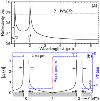
Figure 4(a) shows the reflectivity curve calculated with RCWA from a semi-infinite gold grating (practically m) under normal incidence (with the frequency-dependent permittivity data of gold taken from Ref. HandBook, ). As a reference, the dashed line is the curve with being the Fresnel reflectivity from a flat gold surface ( in the wavelength range m) and the slit width. Compared with this reference curve, the anomalous reflection phenomenon from the grating is obvious. Generally the reflectivity is less than except that near the Wood’s anomalies ( being integers), is close to unity.
Figure 4(b) shows the charge density function on the upper surface () for an arbitrary wavelength in the range. This function correctly shows that the incident wave indeed causes significant inhomogeneous charges on the grating surface with the charges highly accumulating near the slit corners, which is excellently consistent with the charge distribution pattern predicted in Fig. 2(d). At a time when is toward at , we have predicted in Fig. 2(d) that the phase of the charge pattern is constant, equal to (negative charges), on the left half surface , while for , the phase is (positive changes). Figure 4(b) shows that this prediction is largely correct except that the calculated phases are slightly displaced from the predicted phases and by in most regions on the surface. The phases near the slit corners are closer to the predicted values. Our calculations show that the charge patterns are nearly the same for any wavelength with no resonance, and the phase shift decreases with increasing , i.e., for . Therefore, the calculations indeed confirms the picture of charge accumulation and oscillation on the subwavelength lattice in Figs. 2(c) and 2(d). Apparently, the period of the charge pattern in Fig. 4(b) is strictly equal to the lattice constant and is irrelevant to the dispersion property of CSPs in Eq. (1). By performing RCWA calculations on gratings made of conductors with Re or perfect conductors with Im, we found that the main features of the charge patterns remain unchanged.
To understand the anomalous reflection for in Fig. 4(a), we may simply consider that, as we mentioned before, the wavelet in Fig. 2(d) consists of two contributions, , with corresponding to regular Fresnel reflection () and corresponding to the emission of light from dipole along the backward direction . Without charge accumulation, we have and the reflection should obey the Fresnel theory . When charges appear at the slit corners, it can be verified by RCWA that is strengthened much faster than (for ). Then the effective strength of becomes larger than . Consequently, completely cancels , and also partially offsets . Thus, the net effect is that the overall reflectivity is smaller than .
When is reduced to be less than (or close to) the grating period , some of the external wavevectors in Eqs. (III) become (or tend to be) real, and the corresponding diffracted waves become non-evanescent. Then the diffraction effect appear, which can significantly changes the reflectivity (particularly at the Wood’s anomalies ). The details in the diffraction range are discussed in the Appendix since they no longer belong to subwavelength optics. But, it is worth emphasizing again here that the diffraction effect is absent for the entire long wavelength range , where the subwavelength charge patterns are always nearly the same as that in Fig. 4(b).
V Finite-thickness gratings
In Fig. 2 we have indicated that the dipole also emits a wavelet in the slit toward [see in Fig. 5(a), which may also include a portion of the incident wave directly transmitted into the slit]. Due to the waveguide constraint, tends to be a plane wave inside the slit, i.e., , where . Similarly, this wave drives electrons on the slit walls to oscillate, resulting in two SCDWs and (with ) on the two opposite walls, respectively. The SCDWs and the wave propagate along and attenuate gradually due to the absorption of the conductor. If the grating is extremely thick, these waves can be completely absorbed before reaching the bottom surface, which corresponds to the semi-infinite case.
If the grating is thin enough, the SCDWs on the walls can reach the exit surface without significant absorption. Then in a similar way, the moving charges can be impeded at the lower slit corners, leading to another large oscillating dipole , as shown in Fig. 5(a).PRA can give a strong feedback to the upper surface by emitting a wavelet propagating upward. also corresponds to two SCDWs, , on the two walls, which are the back-bounced SCDWs of the waves by the bottom corners. If is in phase with at , it enhances . The enhanced subsequently strengthens , , , , and so on. Then a Fabry-Perot-like resonant state is formed, with and forming a standing wave in the slit. Under this condition, is largely offset by in the far fields, leading to minimized backward reflection. Figure 5(b) shows the zero-order reflectivity curve of a gold grating with thickness m. Compared with Fig. 4(a), one can see that Figure 5(b) indeed shows a number of reflection dips corresponding to Fabry-Perot resonance.
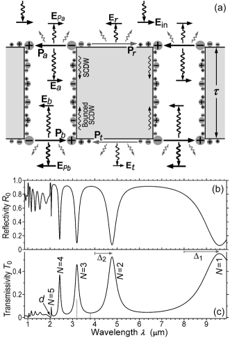
At the exit surface [Fig. 5(a)], dipoles and also emit wavelets towards the outside of the slit. For , only the wavelets and can propagate along (while the oblique wavelets again form evanescent waves). Unlike the case above the upper surface where contains specular reflection, here wavelet is purely emitted from dipole . For , the strength of () is much stronger than that of (), so the transmitted wave is dominated by . Consequently, the energy of the transmitted wave is highly localized near the exit opening. For long wavelengths , such a “near-field focusing” effect can achieve a focusing width far smaller than , which has potential applications in nano-focusing/beaming, lithography, etc. In the far-field region, however, this effect disappears as the transmitted beam becomes a plane wave.McNab
At resonant wavelengths, since the strength of wavelet is maximized, the zero-order transmissivity is also maximized,PRA as can be seen in Fig. 5(c), where each reflection dip exactly corresponds to a transmission peak (also see similar results from finite-difference time-domain calculations in Ref. NGarcia, ).
If the waves and are ideal plane waves with wavevector , Fabry-Perot resonance should occur at ( the resonance order) except that resonant peaks with are suppressed by the diffraction effect.PRA However, the actual resonance wavelength is always redshifted, , where the redshift may vary (slowly) with , , , and . One reason for the redshift is that the standing wave is distorted near the two ends of the slit [see Fig. 6(b)]. One may refer to Ref. Suckling, for discussions of other possible mechanisms. Here note that due to the redshift, the spatial period of the (sinusoidal) SCDWs on the wall is less than the incident wavelength by approximately , i.e., they are also subwavelength charge waves. Based on , thick (and highly conducting) gratings () have many resonance wavelengths in the non-diffraction range , as experimentally demonstrated in Ref. rWent, .
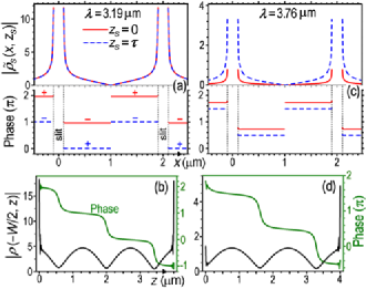
In Figs. 6(a) and 6(b), the computed charge density distributions at resonant wavelength are well consistent with the picture of Fig. 5(a). In Fig. 6(a), the two surface charge patterns are very similar to that in Fig. 4(b), which confirms the existence of the large dipoles and in Fig. 5(a). Note that the charge densities in Figs. 6(a) and 4(b) are in the same (arbitrary) unit. Therefore, the charge densities near the slit corners are much higher in Fig. 6(a) than in Fig. 4(b) due to the Fabry-Perot resonance/enhancement. As also shown in Fig. 6(a), in thin gratings where the attenuation of the charge density waves on the slit walls is negligible, the two SCDWs are almost identical except that for odd resonant orders , they have a phase difference . For relatively thicker gratings, the strength of drops with increasing . For m, almost disappear while tends to be the same as that in Fig. 4(b).
Figure 6(b) correctly reveals that on the slit walls, the charge density waves with approximately stepped phases are nearly standing waves. Here the profile also shows high accumulation of charges at the slit corners that are (always) in phase with .PRA
In Fig. 5(a), if not in phase with (and ) at , it suppresses the strengths of and and influences their phases. Consequently the strengths of the charge waves on the slit walls are also reduced, leading to a weaker dipole and weak transmissivity. This mechanism is clearly shown in Figs. 6(c) and 6(d) at a non-resonant wavelength. Compared with Figs. 6(a) and 6(b), the charge densities at the slit corners all drop significantly for both and , particularly at the upper corners. Meanwhile, the phases of the charge waves are also altered so that no resonance is formed. As stated above, without surface charges, the reflectivity from the upper surface should be the Fresnel reflectivity . Here one can see from Figs. 6(c) and 6(d) that at non-resonant wavelengths, the strengths of and at the upper surface are very small, and then the reflectivity in Fig. 5(b) is indeed very close to in most of the non-resonant wavelength range. For the same wavelength, the non-resonant reflectivity in Fig. 5(b) is much stronger than that in Fig. 4(a) where charge oscillation is heavily involved. This further proves the essential role charge oscillation plays in extraordinary light scattering from metamaterials.
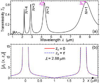
As mentioned above, perfect conductors with Im and conductors with Re do not support CPSs. However, we have demonstrated in Ref. PRA, that 1D gratings with Re may still show similar extraordinary light transmission although the transmissivity is relatively lower.Lezec1 Here we use RCWA to simulate the transmission through a nearly perfectly conducting grating with a large constant imaginary permittivity . Based on this value, the wavevector in Eq. (1) is almost accurately equal to , so CSPs should not exist. However, our calculations show that all the major properties in this case are almost identical to that of regular metallic gratings. For example, Figure 7(a) shows the transmissivity curve calculated with the same geometrical parameters in Fig. 5(c), while Figure 7(b) shows the charge densities on the grating surfaces for the third-order resonance peak. Compared with the reflectivity curve in Fig. 5(c) and the charge density distribution in Fig. 6(a), Figure 7 apparently indicates that the light scattering mechanisms for the perfect-conductor case are the same, and thus are irrelevant to CSPs. In fact, the resonant transmissivity peaks and the charge densities in Fig. 7 are averagely higher than those for the gold grating, indicating that high conductivity can (significantly) enhance the extraordinary scattering effects.
As demonstrated in refs. PRA, and APL, , extraordinary transmission or scattering through 2D hole arrays involve the same mechanisms of light emission and interference except that the tunneling of the SCDWs through the holes is different. The details of oblique incidence geometry will be presented elsewhere, but the charge oscillation principle is similar.
VI Nonperiodic structures
From the above demonstrations, it becomes obvious that charge oscillation-induced light emission and interference are a fundamental and universal mechanism underlying various extraordinary light scattering processes from conducting structures although these processes may also involve other mechanisms simultaneously (e.g. cavity resonance). The only basic requirement for this mechamism to work is that the structure have free electrons. So this mechanism applies to structures of metals, perfect conductors, conductors with Re, semiconductors, etc, but high conductivity can significantly enhance the anomalous scattering effects.
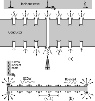
This mechanism also applies to nonperiodic structures.NonPeriodic From Fig. 2(b) one can see that an isolated single slit also acts as a light source. If the conducting plate has a finite thickness, the exit opening of the slit at the lower surface becomes another strong light source at a Fabry-Perot resonant wavelength, emitting a transmitted beam below the plate.Suckling Compared with the periodic slit array in Fig. 5(a), the waves emitted from a single slit have no interference and thus are completely divergent. If the slit is surrounded by periodic grooves on the entrance surface, as shown in Fig. 8(a), each groove now acts as a light source. Under the conditions that the groove period is less than the incident wavelength and that the Fabry-Perot-like resonance can be achieved simultaneously in both the grooves and the slit, the EM fields above the upper surface become similar to those in Fig. 5(a) with the oblique waves forming evanescent modes. Most importantly, the enhanced backward wavelets from the light sources [ in Fig. 5(a)] significantly reduce the Fresnel reflection (). Accordingly, the backward reflection is reduced while the transmission through the slit can be greatly enhanced (by up to 2 orders in Ref. SlitGroove, ). But, the transmitted beam below the plate is still divergent.
Now if similar grooves are made on the exit surface, the wavelets emitted from the exit opening of the slit also drives free electrons to form oscillating dipoles at the openings. Thus, they also become light sources. Similarly, the oblique wavelets emitted from the slit opening and the grooves on the exit surface tend to form evanescent waves, giving rise to a narrow and directed transmitted beam below the slit opening. However, the dipoles on the upper entrance surface are formed and driven mainly by the wide incident wave while those on the exit surface result only from the wavelets emitted from the dipole of the single slit. Therefore, the strengths of the light sources on the exit surface decrease quickly with increasing distances of the grooves from the slit. Due to this reason, the transmitted beam cannot be completely collimated since the oblique wavelets cannot be completely suppressed. Meanwhile, the grooves on the exit surface have little influence on the overall transmission efficiency.SlitGroove
Obviously, the picture illustrated in Fig. 8(a) can also explain enhanced light transmission and directed nanobeaming through a single aperture surrounded by circular grooves in the 2D case except that the cavity resonance mechanisms in the aperture and in the circular grooves may be different and the directions and distributions of the light sources near the groove edges are more complicated.r3
As another nonperoidic structure example, it is known that when one end of a conducting nanowire is illuminated by a narrow-wavefront beam (with the electric field being polarized along the wire), the other end that is not illuminated can emit light, as schematically illustrated in Fig. 8(b). The common explanation of this phenomenon is that light is transferred by CSPs on the wire surface.Nanowire1 However, it is found that this phenomenon is more pronounced in the low-frequency (e.g. terahertz) range, where most metals become nearly CSP-free perfect conductors. In particular, Wang and MittlemanNanowire2 have experimentally demonstrated that in the terahertz range ( mm), the wave modes on metallic nanowires have a dispersion trend that is opposite to that of CSPs.
In fact, according to our charge oscillation picture, the basic mechanism underlying light transfer on nanowires is very simple. In Fig. 8(b), the incident wave drives free electrons near the left input end to oscillate. The agitated electrons then propagate outside the illumination area towards the right side as a SCDW. At the other end the propagating charge wave is discontinued, giving rise to a strong charge accumulation there. The oscillation of these charges them emit new light near the exit end. Meanwhile, the charge wave is bounced back. When the bounced charge wave is in phase with the forward wave (and the incident wave) at the input end, Fabry-Perot resonance occurs. This is very similar to the charge movement on the slit walls in Fig. 5(a). In general, the resonant wavelength here also has a redshift. Accordingly, the standing charge wave on the wire surface is a subwavelength wave (), and based on Fig. 1, it generates little radiation loss when propagating on the wire. The Fabry-Perot resonance and the subwavelength charge patterns (proportional to the strengths of the near fields) indeed have been demonstrated both experimentally and theoretically.Nanowire1 ; Nanowire2 ; Nanowire3 . Interestingly, our calculations show that a charge wave propagating in the unilluminated region of a flat/straight conducting surface (including the slit wall and the straight wire) is always a subwavelength SCDW, which indicates that the general SP picture elaborated in the literature, light subwavelength SCDWs light, is indeed correct except that the SCDWs are spoof SPs and do not necessarily have the dispersion property of Eq. (1).
According to this picture, the conductivity of the nanowire is the dominant factor determining the propagating distance of the charge waves and the efficiency of light transfer. This explains the remarkably high transfer efficiency in the long-wavelength range where most metals are highly conducting. To further confine the near fields so as to reduce the radiation loss (caused by possible deviations of the actual charge waves from ideal subwavelength standing waves), one may activate charge waves in grooves and guide them to propagate inside the grooves. In these cases, the charge waves are channel spoof SPs ChannelSP that may have longer propagating distances.
From Fig. 8(b) it is obvious that to achieve high transfer efficiency, the diameter (vertical dimension) of the wire should be much smaller than the incident wavelength so that the agitated charge waves on the top and bottom of the wire have nearly the same phase. Otherwise, the charge waves with different phases will quickly mix together and thus offset each other outside the illuminated region, leading to a short propagation distance. This explains why light transfer is remarkable on nanowires. With respect to this effect, it is expected that a thin conducting slab would be more efficient since it can enhance the input coupling efficiency and reduce the electrical resistance without causing phase differences.
Note that in Fig. 2(c), when the moving electrons are stopped at the slit corners, they also have a tendency to be bounced back, similar to the moving electrons on the nanowires in Fig. 8(b) [and on the slit walls in Fig. 5(a)]. The difference in Fig. 2(c) is that the bounced back charges are suppressed by the incident electric field since the driving force provided by is always opposite to this tendency, while on the nanowire of Fig. 8(b), is absent except at the input end.
VII Summary
By numerically calculating the SCDWs on gratings, we have demonstrated that the incident wave can drive free electrons to accumulate and oscillate near the slit corners to form new light sources. These light sources then emit new wavelets. For periodic subwavelength structures (), the oscillating charges form subwavelength charge patterns (i.e., spoof SPs) and the wavelets emitted from them destructively interference with each other to form evanescent wave modes near the surfaces. Usually combined with other mechanisms (e.g. Fabry-Perot or cavity resonance), the spoof SPs can lead to anomalous light reflection, transmission, or scattering. The spoof SPs are mainly a geometrical effect and generally do not have the dispersion properties of CSPs. Note that in the literature, the SP-like modes on metamaterials with finite conductivity were widely assumed to be CSPs, while only those on perfectly conducting structures were believed to be spoof SPs. Here we have demonstrated that they are all spoof SPs. (For transmission of acoustic waves through gratings,Ming ; Ming2 the counterpart of charge oscillation is the mechanical vibration of the structured medium, particularly near the corners and edges, that emits acoustic wavelets.)
We also illustrated that the same mechanism of charge oscillation-induced light emission and interference applies to all structures with free electrons (including perfect conductors and nonperiodic structures). Thus, the spoof SP picture represents a basic and universal mechanism of light scattering from conducting nanostructures. The guideline provided by this mechanism is that in designing novel nano-metamaterial devices, there is no CSP excitation constraint, but one needs to precisely design the geometrical parameters of the devices so as to accurately control the locations of the new light sources (including maximizing the strength of various resonance processes if involved) and their interference. Meanwhile, choosing highly conducting materials is generally another requirement for enhancing the anomalous scattering effects.
ACKNOWLEDGEMENTS
This work was supported by grants from the NSFC (Grant Nos. 10625417, 50672035, and 10874068), the MOST of China (Grant Nos. 2004CB619005 and 2006CB921804), and partly by the ME of China and also Jiangsu Province (Grant Nos. NCET-05-0440 and BK2008012). X.R.H was supported by the U.S. Department of Energy, Office of Science, Office of Basic Energy Sciences, under Contract No. DE-AC-02-98CH10886. We thank Yong Q. Cai for helpful discussions.
*
Appendix A Charge patterns in the diffraction range for 1D gratings
One might intuitively think that for normal incidence with the electric fields parallel to the surface in Fig. 2(c), the charge pattern on the surface should remain the same even if , as provides the same driving force. However, the free electrons on the grating surface are driven by both the incident wave and the wavelets emitted from the charges/dipoles. The latter may significantly influence the charge distribution (to achieve self-consistency of the system) when .
Figure 9 shows the charge patterns in the short-wavelength range ( close to or below ) for the semi-infinite grating of Fig. 4(a). To understand these patterns, recall in Sec. III that the th-order wave components () above the grating can be written as and , respectively for normal incidence, where . By symmetry, . So these two waves form a standing wave . Accordingly, there exists a standing SCDW corresponding to this wave on the metal surface (but discontinued in the slit gap). For , the propagating factor of the wave becomes a decaying factor along , where is the decaying coefficient. Therefore, the wave is an standing evanescent wave under this condition. For (so that ), all the waves except for are evanescent, so they all have weak strengths. The charge pattern in Fig. 4(b) is the collective contributions from a large number of charge wave components , and this pattern (as well as the collective near fields of the wavelets emitted from the dipoles) coincides with the grating lattice.
When decreases toward from above, the first-order wave tends to be strengthened as its decaying coefficient decreases. Compared with Fig. 4(b), one can see in Fig. 9(a) the appearance of the standing SCDW component superimposed on the overall charge pattern that is similar to that in Fig. 4(b). (Here the charges are influenced by the near fields even if the wave is evanescent in the far fields.) Meanwhile, the phase shift indicated in Fig. 4(b) increases to in Fig. 9(a) due to the phase of the complex constant .
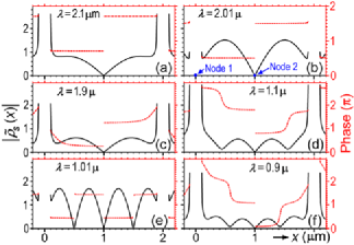
The wavelength corresponds to the first-order Wood’s anomaly.PRA Under this condition, the wavelets emitted from two adjacent units of the grating along the horizontal direction have a phase difference of according to Fig. 2(c), which corresponds to a special Bragg diffraction condition. Then the strength of wave is maximized and becomes outstanding among other components, as can be verified by RCWA. Therefore, the charge pattern in Fig. 9(b) is dominated by the corresponding charge wave . Here one (virtual) node (Node 1) of this standing SCDW is located at (), the middle of the slit [while the other node (Node 2) is at ()]. Node 1 significantly suppresses the charge densities at the two slit corners (because the nodes of a standing wave have zero amplitudes), so the strength of the dipole [see Figs. 2(c) and 2(d)] is minimized. As discussed in Figs. 6(c) and 6(d), when the strength of is very small, the reflectivity should approach the Fresnel reflectivity . But note that in Fig. 9(b), the charge pattern also contributes positively to the reflectivity [equivalent to the increase of in Fig. 2(d) although it has a phase difference from the incident wave]. This is the reason why in Fig. 4(a) the reflectivity at Wood’s anomaly wavelengths is even higher than . Note that the first-order Wood’s anomaly in Fig. 4(a) is slightly red-shifted from to m.
When decreases to m in Fig. 9(c), the wave is still a propagating mode, but its strength decreases as the diffraction condition deviates from the Bragg condition. Meanwhile, the wave begins to gain strength, which modifies the stepped phase profile. When further decreases toward in Fig. 9(d), the wave becomes appreciable. At the second-order Wood’s anomaly m (also slightly red-shifted from ), this wave is maximized [Fig. 9(e)]. For [Fig. 9(f)], the third-order wave begins to show strengths, and so on. Thin gratings have similar properties, but these effects are meanwhile mixed with the resonance in the slits.
Overall, we may call the short-wavelength range the diffraction range, where the diffraction effect of the 1D lattice appear, particularly at the Wood’s anomalies. In the diffraction process, it is interesting that the incident energy is largely back reflected rather than diffracted although the corresponding diffracted waves become non-evanescent, as can be seen from Fig. 4(a). This is also true in Figs. 5(b) and 5(c) for the thin grating, where the reflectivity is averagely very high in the entire diffraction range while the transmissivity (particularly at the Fabry-Perot resonant transmission peaks) is much lower than that in the non-diffraction range .
References
- (1) T. W. Ebbesen, H. J. Lezec, H. F. Ghaemi, T. Thio, and P. A. Wolff, Nature (London) 391, 667 (1998).
- (2) W. L. Barnes, A. Dereux, and T. W. Ebbesen, Nature (London) 424, 824 (2003).
- (3) C. Genet and T. W. Ebbesen, Nature (London) 445, 39 (2007).
- (4) X. J. Yu and H. S. Kwok, J. Appl. Phys. 93, 4407 (2003).
- (5) X. Zhang and Z. Liu, Nature Mater. 7, 435 (2008).
- (6) J. R. Sambles, G. W. Bradbery, and F. Yang, Comtemp. Phys. 32, 173 (1991).
- (7) K. Wang and D. M. Mittleman, Phys. Rev. Lett. 96, 157401 (2006).
- (8) H. J. Lezec and T. Thio, Opt. Express 12, 3629 (2004).
- (9) X. R. Huang, R. W. Peng, Z. Wang, F. Gao, and S. S. Jiang, Phys. Rev. A 76, 035802 (2007).
- (10) M. Sarrazin and J. P. Vigneron, Phys. Rev. E 68, 016603 (2003).
- (11) M.-H. Lu, X.-K. Liu, L. Feng, J. Li, C.-P. Huang, Y.-F. Chen, Y.-Y. Zhu, S.-N. Zhu, and N.-B. Ming, Phys. Rev. Lett. 99, 174301 (2007).
- (12) G. Gay, O. Alloschery, B. Viaris de Lesegno, C. O’dwyer, J. Weiner, and H. J. Lezec, Nature Phys. 2, 262 (2006).
- (13) P. Lalanne and J. P. Hugonin, Nature Phys. 2, 551 (2006).
- (14) N. Garcia and M. Nieto-Vesperinas, J. Opt. A: Pure Appl. Opt. 9, 490 (2007).
- (15) B. C. Cullity and S. R. Stock, Elements of X-Ray Diffraction (3rd edition, Prentice Hall, Uppe Saddle River, 2001), p. 123.
- (16) M. Born and E. Wolf, Principles of Optics (Cambridge Univ. Press, Cambridge, 1999).
- (17) J. B. Pendry, L. Martín-Moreno, and F. J. Garcia-Vidal, Science 305, 847 (2004).
- (18) F. J. García de Abajo and J. J. Sáenz, Phys. Rev. Lett. 95, 233901 (2005).
- (19) M. G. Moharam, E. B. Grann, D. A. Pommet, and T. K. Gaylord, J. Opt. Soc. Am. A 12, 1068 (1995).
- (20) P. Lalanne and G. M. Morris, J. Opt. Soc. Am. A 13, 779 (1996).
- (21) Handbook of Optical Constants and Solids, edited by E. D. Palik (Academic, Orlando, 1985).
- (22) S. J. McNab and R. J. Blaikie, Appl. Opt. 39, 20 (2000).
- (23) J. R. Suckling, A. P. Hibbins, M. J. Lockyear, T. W. Preist, J. R. Sambles, and C. R. Lawrence, Phys. Rev. Lett. 92, 147401 (2004).
- (24) H. E. Went, A. P. Hibbins, J. R. Sambles, C. R. Lawrence, and A. P. Crick, Appl. Phys. Lett. 77, 2789 (2000).
- (25) Z. J. Zhang, R. W. Peng, Z. Wang, F. Gao, X. R. Huang, W. H. Sun, Q. J. Wang, and M. Wang, Appl. Phys. Lett. 93, 171110 (2008)
- (26) T. Matsui, A. Agrawal, A. Nahata, and Z. V. Vardeny, Nature (London) 446, 517 (2007).
- (27) F. J. García-Vidal, H. J. Lezec, T. W. Ebbesen, L. Martín-Moreno, Phys. Rev. Lett. 90, 213901 (2003).
- (28) H. Ditlbacher, A. Hohenau, D. Wagner, U. Kreibig, M. Rogers, F. Hofer, F. R. Aussenegg, and J. R. Krenn, Phys. Rev. Lett. 95, 257403 (2005).
- (29) T. Laroche and C. Girard, Appl. Phys. Lett. 89, 233229 (2006).
- (30) S. I. Bozhevolnyi, V. S. Volkov, E. Devaux, J.-Y. Laluet, and T. W. Ebbesen, Nature (London) 440, 508 (2006).
- (31) J. Christensen, L. Martin-Moreno, and F. J. Garcia-Vidal, Phys. Rev. Lett. 101, 014301 (2008).