Exchange effects in spin polarized transport through carbon nanotube quantum dots
Abstract
We investigate linear and nonlinear transport across single-walled carbon nanotube quantum dots weakly coupled to spin-polarized leads. We consider metallic tubes of finite length and small diameter, where not only forward scattering contributions of the Coulomb potential, but also short-ranged processes play an important role. In particular, they induce exchange effects leading for electron fillings either to a non-degenerate groundstate of spin or to a triplet groundstate. In the linear regime we present analytical results for the conductance - for both the and the triplet groundstate - and demonstrate that an external magnetic field is crucial to reveal the spin nature of the groundstates. In the nonlinear regime we show stability diagrams that clearly distinguish between the different groundstates. We observe a negative differential conductance (NDC) effect in the groundstate for antiparallel lead magnetization. In presence of an external magnetic field, spin blockade effects can be detected, again leading to NDC effects for both groundstates.
pacs:
73.63.Fg, 72.25.-b, 73.23.Hk, 85.75.-dI Introduction
Since their discovery by S. Iijima and T. Ichihashi Iijima in 1993, single-walled carbon nanotubes (SWNTs) have attracted attention due to their remarkable electronic and mechanical properties Saito ; Loiseau . At low energies, they represent an almost perfect realization of a one-dimensional (1D) system of interacting electrons with an additional orbital degree of freedom due to the sublattice structure of graphene. Accounting for spin and orbital degrees of freedom implies that for nanotubes a shell structure is expected, where each shell can accommodate up to four electrons. In the absence of Coulomb interaction the energy levels are spin degenerate, while the orbital degeneracy is usually lifted due to the nanotube finite length. Coulomb interactions, however, modify this picture. The sublattice structure of graphene gives rise to a distinction between electron interactions on the same and on different sublattices. Therefore, besides the long-ranged forward scattering processes, also short-ranged interaction processes play a role in small diameter tubes Egg ; Odin ; Oreg ; Leo1 . These short-ranged interactions cause in finite size nanotubes exchange effects leading for a tube filling of to a groundstate with either total spin or (a triplet)Leo1 . Signatures of the exchange interactions have indeed been inferred from stability diagrams of carbon-nanotube-based quantum dots Mor1 ; Sap ; Liang . In particular it was shown by Moriyama et al.Mor1 that an applied magnetic field can be used to reversibly change the groundstate from the singlet to one of the triplet states.
Recently, carbon nanotubes have also attracted much attention for their potential applications in spintronic devices Cott . They are particularly interesting because they have a long spin lifetime and can be contacted with ferromagnetic materials. Indeed, spin-dependent transport in carbon nanotube spin valves has been demonstrated by various experimental groups Sahoo ; Man ; Haupt , ranging from the Fabry-Perot Man ; Sahoo to the Kondo regime Haupt .
From the theoretical point of view, spin-dependent transport in interacting SWNTs has been discussed so far in the limit of very long nanotubes Bal , for tubes in the Fabry-Perot regime Peca and for SWNT-based quantum dots Kos ; Wey ; Wey2 . In the three latter works the characteristic four-electron shell-filling could be observed in the stability diagrams. In Kos however, focus was on medium-to-large diameter SWNTs where exchange effects can be neglected. The studies in Wey ; Wey2 are based on the theory by Oreg et al. Oreg , where exchange interactions are treated on a mean-field level, and focus predominantly on shot noiseWey and cotunnelingWey2 effects.
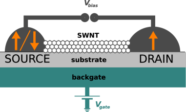
In this work we generalize the previous investigations of Ref.Kos to include the short range Coulomb interactions causing exchange splittings of the six otherwise degenerate (at vanishing orbital mismatch) - filling groundstates. The leads are either parallel or antiparallel spin-polarized and weakly coupled to the SWNT, see Fig. 1.
In the low bias regime we derive analytical formulas for the conductance for both large and small orbital mismatch corresponding to an and groundstate, respectively, at filling. In the high bias regime we numerically calculate the stability diagrams for the two possible groundstates. We show several differences in transport between parallel and antiparallel lead magnetization, as e.g. a negative differential conductance (NDC) effect occurring only for the groundstate and antiparallel magnetization. We further include in the calculations a parallel magnetic field leading to a Zeeman splitting for all states with total spin unequal to zero. It is then possible to observe spin blocking effects due to transport channels that trap the system in the triplet state with . Performing a magnetic field sweep, a groundstate change may be obtained as it has been shown experimentallyMor1 .
The paper is organized as follows. In section II we discuss the relevant features of the low energy Hamiltonian of interacting SWNTs with special focus on the filling .
In section III we describe the set-up and method used to study spin-dependent transport in the sequential tunneling regime. Finally, in section IV, we present our results for the conductance, while in section V we focus on the nonlinear (finite bias) regime.
II The interacting low energy spectrum
II.1 The interacting Hamiltonian
The starting point for a microscopic, but still analytical, treatment of SWNTs is a tight-binding ansatz for the wavefunction of the - electrons on the graphene honeycomb lattice. Including nearest neighbor hopping matrix elements it yields an electron-hole symmetric bandstructure with a fully occupied valence band and an empty conduction band. Since the two bands touch at the cornerpoints of the 1st Brillouin zone, the Fermi-points, graphene is a zero gap semiconductor. Wrapping the considered sheet of graphene, i.e., imposing periodic boundary conditions (PBCs) around the circumference, yields a SWNT and leads to the formation of transverse subbands. For the low energy electronic structure of metallic SWNTs, only the subbands touching at the Fermi-points are of relevance. In the following we consider armchair SWNTs of finite length and impose open boundary conditions (OBCs) at the two ends of the tube, i.e., that the wave function vanishes at the armchair edges. This condition mixes the two inequivalent Fermi points from the underlying graphene first Brillouin zone and yields the linear dispersion relation
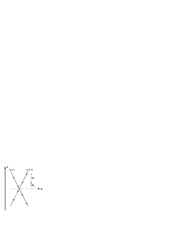
of the finite size SWNT shown in Fig. 2. It is characterized by two linear branches of slope with the Fermi velocity . The allowed quasi-momentum values are given by , where , is the tube length and accounts for the fact that may not be an integer multiple of . The kinetic part of the Hamiltonian, yielding the energy relative to the Fermi-sea, correspondingly reads
| (1) |
where is the level spacing, and is the band offset energy.
Finally creates an electron with momentum and spin in branch and the operator
counts the total electron number in branch and of spin .
The interaction part of the Hamiltonian is given by
| (2) |
where are fermion field operators and we use the Ohno-potential Barford ,
| (3) |
with Ful and Egg is the dielectric constant of graphene. In the next step we express the 3D electron operators in terms of the 1D fermion-fields Leo2
| (4) |
and obtain
| (5) |
Here denotes the two independent Fermi-points, the two sublattices of graphene, and the coefficients of the sublattice wave function are given by for and for . The sublattice wave function itself reads
| (6) |
where is the number of graphene lattice sites identified by the lattice vector , and denotes the graphene honeycomb lattice in real space. Furthermore, is the wavefunction of a carbon atom living on sublattice , identified by the sublattice vector . Upon integrating Eq. (2) over the coordinates radial to the tube axis, one eventually arrives at a 1D interaction potential characterized by density-density and non density-density contribution Leo1 so that the total Hamiltonian reads
| (7) |
With the help of bosonization Del it is possible to diagonalize the density part . Eventually the bosonized and diagonalized Hamiltonian takes the form Leo1 :
| (8) |
Besides the ground state, it accounts for all the possible fermionic and bosonic excitations of a SWNT. The bosonic excitations are described by the first term on the right hand side. The indices refer to total/relative charge/spin modes. The energies are given by
| (9) |
with and
| (10) |
the contribution of the long-ranged density-density processes. Indeed is the sum of the interaction potentials for electrons living in the same (intra) and different (sublattices):
| (11) |
The second summand of (8) is the charging term with the charging energy and also comes from the long range part of the Coulomb interaction. It counts the energy one has to spend to put electrons on the dot, no matter what spin or pseudospin they have. The second line of (8) starts with an exchange term favoring spin alignment. The exchange-splitting,
| (12) |
being proportional to the difference of the Coulomb interaction for electrons on the same and on different sublattices, accounts for the contribution of short range processes. The next term in (8) reflects the energy cost for adding electrons of the same spin band in the same branch, i.e., the Pauli-principle, where the correction is
| (13) |
Finally, the last term accounts for a possible band-mismatch, see Fig. 2.
The eigenstates of are spanned by
| (14) |
Here denote the fermionic and the bosonic configuration, respectively, such that the state has no bosonic excitation. The fermionic configuration is given by the number of electrons in each branch with a certain spin . These eigenstates will be used to calculate the contribution of the non-density part of the interaction, i.e., . Away from half-filling, they only couple states close in energy and one is allowed to work with a truncated eigenbasis (we check convergence of the results as the basis is enlarged). As shown by Yoshioka and Odintsov Yoshi , for long SWNTs a Mott-insulating transition is expected to occur at half-filling due to umklapp scattering. As found in Ref. Leo1 umklapp processes acquire increasing weight as half-filling is approached also for finite size tubes, a possible signature of the Mott instability, and the present theory breaks down. In recent experiments Des the observation of the Mott transition in SWNT quantum dots was claimed.
II.2 Low energy spectrum away from half-filling
The low energy regime is where the energies that can be transferred to the system by the bias voltage and the temperature stay below . This means no bosonic excitations are present, i.e., , and also no fermionic excitations are allowed, i.e., the four bands will be filled as equal as possible: . Our starting point are the eigenstates, Eq. (14), of the Hamiltonian in Eq. (8), which accounts for the kinetic and the density part of the full Hamiltonian. Now we have to split the examination into two cases.
At first we consider states with total charge equal to , and . Those are unambiguously described by the fermionic configuration because they are not mixed by the exchange effects.
The only impact of the short-range interaction terms on these states is given by
an energy penalty for double occupation of one branch , a common shift for all eigenstates with fixed . Therefore we are left with Leo1
| (15) |
for the energy. If , states with the maximum allowed number of electrons in the branch will be the groundstates. For the pseudospin branches are equally occupied, yielding an unique groundstate. The corresponding configuration is taken as reference configuration for the cases. The lowest lying states for are presented in Fig. 3. E.g., for the case we obtain four possible states corresponding to . For simplicity we introduce for the states with an unpaired electron in the branch the notation . For electrons in the branch we set .
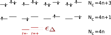
Analogously, neglecting exchange effects and setting for the moment, the groundstates for the filling are represented by the six states , , , , and , where, e.g., means two electrons with spin one on each branch and . Here the different fermionic configurations mix under the influence of the processes and the groundstate structure will change dramatically due to off-diagonal contributions
| (16) |
Diagonalization of the interaction matrix yields the groundstate spectrum as it is shown in table 1. The energies in the table are given relative to .
|
|||||||||||||||||||||
It is clear that the states and will always be excited states, while the spin triplet, , is energy degenerate. Now the question arises which states, the triplet or the state, are the groundstate of the system. In accordance with table 1, the condition for a triplet groundstate is given by:
| (17) |
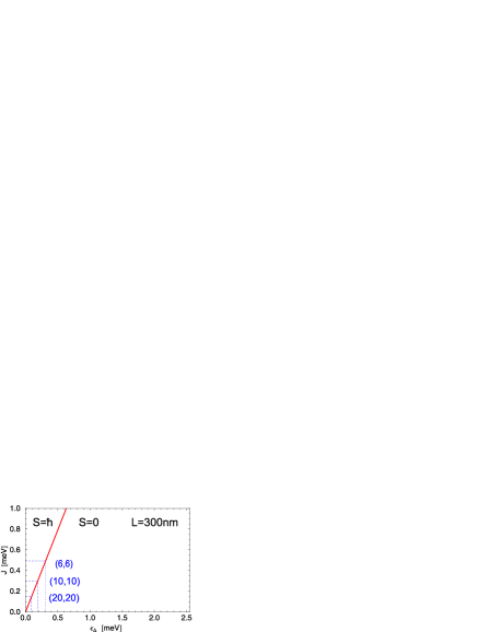
For a dielectric constant it holds and . Hence we find in terms of the level spacing and the tube diameter :
| (18) |
Obviously this makes the triplet groundstate more unlikely compared to the groundstate as it can be seen in Fig. 4. For a (6,6) nanotube of 300nm length, the band-mismatch must be to be in a triplet groundstate. In the experiments Sap ; Liang band-mismatches are of the order of and, as expected from our theory, - groundstates are observed.
III Spin-dependent transport
In this section we discuss the set-up to evaluate spin-dependent transport across a SWNT weakly coupled to leads, see Fig. 1, and the main calculation tools. The Hamiltonian of the full system reads
| (19) |
where denotes the Hamiltonian in the source and the drain contact, respectively. The leads magnetization is accounted for in terms of a Stoner Hamiltonian where the density of states, , for the majority () and the minority () carriers are different. We treat the leads within the wide-band approximation, i.e., we regard the density of states as constant quantities to be evaluated at the leads chemical potentials and . We can thus define the polarization by ():
| (20) |
Moreover, we will consider a symmetric set up and . The total density of states is given by .
We account for the bias voltage in terms of the difference between the electrochemical potentials in the source and drain leads.
Further, in Eq. (19) is the tunneling Hamiltonian which we will treat as a perturbation since weak coupling to the leads is assumed. Finally, describes the influence of the externally applied gate voltage . The gate is capacitively coupled to the SWNT and hence contributes via a term with a proportionality factor.
In order to evaluate the current-voltage characteristics we use the method developed in Ref. Kos where, starting from the Liouville equation for the density matrix of the full system, a generalized master equation (GME) for the reduced density matrix (RDM) of the SWNT is obtained to second order in .
Once the stationary RDM is known, the stationary current through e.g. the source lead is evaluated from the relation
, where is the number operator for electrons in the left lead.
As this procedure with the relevant equations is thoroughly explained in Ref. Kos , we refrain from repeating it here.
The GME can be solved in analytic form in the linear regime, being the focus of
the following Sec. IV. In the nonlinear regime, discussed in Sec. V, the differential conductance is evaluated numerically. Moreover, from here on we will focus on the transition between charge states , mirror symmetric to , as these two transitions are the ones that reveal exchange effects. The remaining transitions and will not qualitatively change due to the presence of short range processes and we hence refer to the discussion in Kos .
If not otherwise specified, we choose nanotubes described by the parameters in table 2:
In order to obtain an groundstate we assume a band-mismatch of meV, whereas for a triplet groundstate we choose .
IV The linear regime
IV.1 Conductance at zero magnetic field
We focus on the conductance formulas for the two cases of tunneling from the groundstates into the groundstate or into the triplet groundstates.
| parameters | label | value |
|---|---|---|
| length | nm | |
| diameter | nm | |
| dielectric constant | ||
| charging energy | meV | |
| level spacing | meV | |
| Coulomb excess energy | meV | |
| exchange energy | meV | |
| orbital mismatch | meV or meV | |
| thermal energy | meV | |
| transmission coefficient | meV |
For the transition the conductances in the case of parallel, , and antiparallel, , magnetized leads are found to be
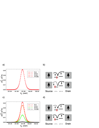
| (21a) | ||||
| (21b) | ||||
with , the Fermi function evaluated at the gate voltage dependent energy difference and the inverse temperature. The parameters and describe the possible asymmetric lead transparencies Kos (hereby, is in second order of the tunneling coupling contained in ). The conductances are shown in Fig. 5a) and 5c) for the symmetric transparencies case and meV. Strikingly, in the parallel magnetized case there is no dependence on the polarization since there is never a blocking state involved in transport, see Fig. 5b). For the antiparallel case, in contrast, transport is limited by the weakest channel (when there is a - electron on the dot) and one can drive the conductance to zero by tuning the polarization to . This feature is explained in Fig. 5d).
For the case of the triplet groundstate we face a completely new situation. First, we have for filling four degenerate states available because the band-mismatch has been chosen to be zero. Secondly, we couple to three different states in the case of rather than to just one. However, the conductance plots do not qualitatively change as it may be seen in Fig. 6a) and 6c). The conductance formulas read:
| (22a) | ||||
| (22b) | ||||
Compared to Eqs. (21a), (21b) the prefactor changed from to 3 due to the three involved triplet states. The quantity is the difference between the triplet and the - groundstate energies. In addition, the denominator in the term containing the Fermi-functions has also changed to account for the degeneracy of the - filling states. The qualitative behavior, however, does not change compared to the case of an groundstate, such that one cannot determine the spin nature of the groundstate from these plots alone.
IV.2 Conductance in the presence of an external magnetic field
In this section we consider the influence of an externally applied magnetic field (Zeeman-field) which clearly reveals the character of the groundstate for and, moreover, may even change the groundstate depending on the field strength. The field causes an additional Zeeman energy to states with a spin-component . The sign is negative if the concerned state in the tube is parallel to the external field and positive if antiparallel. Thus, the chemical potential differences appearing in Eqs. (21a), (21b), (22a) and (22b) will be shifted by . We use the convention and . Furthermore, in order to improve the readability, we introduce the abbreviation . The conductances for the antiparallel set-up are
| (23a) | |||
| and | |||
| (23b) | |||
We do not find qualitative differences with respect to the zero magnetic field case: the conductances decrease in both cases with increasing polarization. In the following, we will therefore only focus on the parallel case, where we find interesting behavior for small Zemann splittings. The conductance formulas for parallel lead magnetization take the form
| (24a) | |||
| and | |||
| (24b) | |||
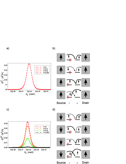
The corresponding plots can be seen in Figs. 7a) and 8a). In these calculations we considered a small magnetic field of T which equals in magnitude the thermal energy of meV. This provides a situation with a finite occupation probability for all included states. Specifically, this means that also states containing - electrons will be populated, but the population of states containing - electrons will be preferred.
The first thing we observe in both Fig. 7a) and 8a) is that the once degenerate curves in Figs. 5a) and 6a) now split into distinct curves for the four different polarizations. Moreover, the peaks of the curves corresponding to less polarized leads continuously move to higher gate voltages. Finally the conductance decreases/increases with increasing polarization for the cases, respectively. Let us examine the results starting with the - groundstate.
We will divide the analysis in two cases, slightly polarized leads and strongly polarized leads.
For only slightly polarized or non-polarized leads the situation is intricate as we have to deal with competing processes. On the one hand there is a highly populated state and a slightly populated state in the tube. From this point of view, the system prefers - electrons to tunnel into the state and to leave the dot subsequently such that the tube always remains in the preferred state (Fig. 7, sketch b), upper left panel). Only rarely, the - electron tunnels out, as this would result in a spin-flip to the disfavored state (Fig. 7, sketch b), lower left panel).
On the other hand, entering of - electrons is suppressed compared to transport of - electrons, not so much by the small polarization, but mainly due to the Zeeman splitting in the involved Fermi-functions: The chemical potential for - electrons exceeds the one for - electrons by such that at any gate voltage. However, in the end it will be a mixture of mainly - electrons and some - electrons responsible for transport. This can also be seen by the fact that the curves for small polarizations are shifted to higher gate voltages which accounts for the higher chemical potential of the - electrons. In addition, the total amplitude of the conductance is decreased compared to the case without the magnetic field, Fig. 5a), as there is always a limiting element - either the small Fermi-function or the small population - involved.
In the case of highly polarized leads we face the situation where there are very few - electrons in the leads. As temperature provides a small, but nonzero population of the slightly excited state , current mainly flows via the polarization-favored - electron channel. Since the chemical potential, the increment of the Fermi-functions, is smaller than in the former case the transition takes place at slightly lower gate voltages. The situation again is visualized in the sketch b) of Fig. 7, in the upper and lower right panel.
At the triplet resonance we observe not only quantitative, but also qualitative changes. The plot can be seen in Fig. 8a) and all relevant tunneling processes are sketched in Fig. 8b). Let us again start with unpolarized or just slightly polarized leads. Due to a large population of the spin states in the case and of the state in the case transport is mainly mediated via the majority charge carriers, i.e. - electrons (Fig. 8b), upper right panel). However, the resulting current is smaller than in the case without magnetic field since it is harder to make use of the - electrons that are still largely at disposal in the leads.
A high polarization decreases the number of - electrons in the leads in favor of the - electron number, and such transport via the already preferred channel is strongly enhanced.
As a consequence, the conductance by far exceeds the conductance without magnetic field and polarization.
This effect should be detectable in an experimental setup and would give a possibility to distinguish between a triplet groundstate and a groundstate.
V The nonlinear regime
In the finite bias regime also excited states become available and, due to the resulting high number of involved states, it is necessary to calculate the current numerically. We show the current and the stability diagrams - the differential conductance as a function of the gate and the bias voltage.
The stability diagrams give a clear indication whether the involved groundstate in the transition is the state or the triplet. In the case of antiparallel lead magnetization we find negative differential conductance (NDC) for transitions involving the state. We also observe NDC for transitions involving the state or the triplet if an external magnetic field is applied.
The current as a function of the gate and the bias voltage is shown in Fig. 9a) for the groundstate and in Fig. 9b) for the triplet groundstate.
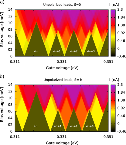
All states with up to one bosonic excitation have been included in the calculation. A 4-electron periodicity of the Coulomb diamonds is clearly seen. The change in color indicates a change in current and therefore the opening of a new channel. At high bias a smearing of the transitions due to the multitude of bosonic excitations is observed. In the remaining of this section we focus on the gate voltage region relevant for the transitions. In the plots of the differential conductance reported in the following we did not include the bosonic excitations to avoid a multitude of transition not relevant for the coming discussion. A polarization is chosen.
V.1 Differential conductance at zero magnetic field
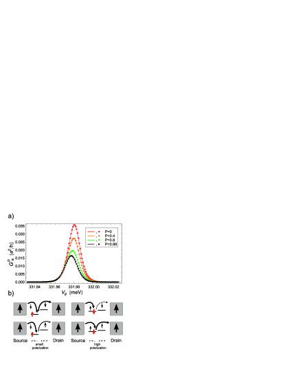
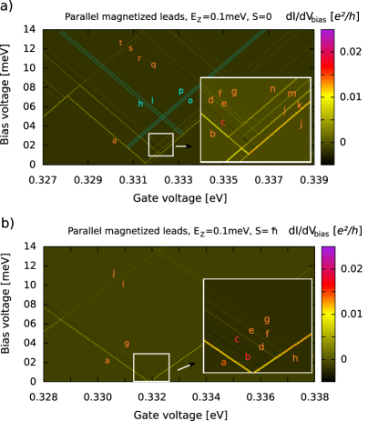
Figs. 10a) and Fig. 10b) show the stability diagrams for parallel and antiparallel lead magnetization, respectively, for the case of the groundstate. The two transition lines h and e were emphasized by a dashed line because these lines are so weak that it was not possible to resolve them together with the other stronger lines. The most obvious difference between the parallel and the antiparallel setup is the weakness of all transition lines beyond the triplet occupation (line b) for antiparallel lead magnetization. Moreover an NDC line, (line b), not present in the parallel magnetization case, is observed.
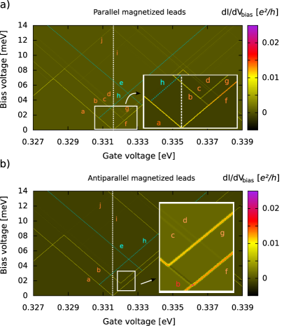
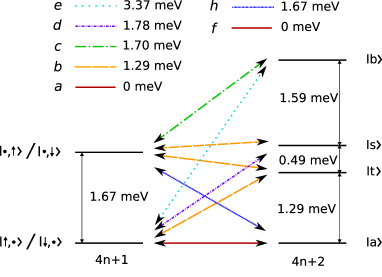
In order to explain the line positions in Fig. 10a),b) we provide a schematic drawing in Fig. 11 which is based on a bias trace at the particular gate voltage which aligns the groundstates (white vertical lines in Fig. 10). The differently colored arrows stand for new transport channels that open at certain bias voltages. The channels open in the order of a to e for transitions from (dashed arrows) and f to h for transitions from (solid arrows). Sometimes opening of a new channel also opens other channels that have been blocked before and one does not see distinct lines for these transitions. Fig. 11 relates the concerned transitions to the required bias voltages. Moreover, the line g stands for transitions between the triplet and the states, i.e., it is a transition between excited states.
To explain the NDC in Fig. 10b) which follows upon line b in the range between lines f and line g, we observe that – in correspondence of the b line – below the resonance only the transitions from to the state is possible. Above resonance also the triplet is accessible. For the case of antiparallel polarization, both provide only weak transport channels: below the resonance
transport is mostly mediated by - electrons (see also sketch of Fig. 5) which are minority electrons for the source contact; above resonance, after some tunneling processes the system will always end up in the state which is a trapping state.
Just at the exact resonance, the thermal energy allows electrons to tunnel forth and back, i.e., a - electron has the possibility to tunnel back into the source contact and transport is slightly enhanced. Once the bias voltage exceeds the exact resonance the trapping state gets occupied for long times and the current diminishes again.
The fact that the transition serves as the major transport channel once it has been opened is also the
reason why all transition lines above line b are so weak.
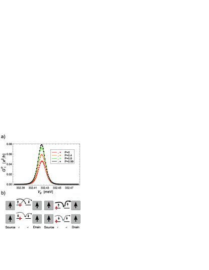
In Figs. 12a) and 12b) the stability diagrams for the triplet groundstate are shown.
They look a lot simpler than the ones in Fig. 10 due to the absence of a band-mismatch, causing a degeneracy of all four filling groundstates. Line a is the groundstate to groundstate transition. Lines b to d indicate transitions from the groundstates to , and , respectively.
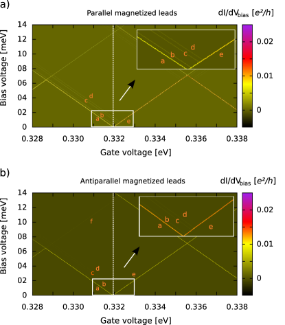
They come in the expected order, at an applied voltage equal to , and , as it is shown in table 1. Line e stands for the transition from the triplet to one of the groundstates.
For the antiparallel setup, Fig. 12b), we may see the same effect as we have observed in Fig. 10b), i.e., all lines beyond the transition to the triplet decrease in intensity.
Since the triplet is the groundstate, this means all excitation lines are weak and may not be resolved in the figure.
V.2 Differential conductance in parallel magnetic field
Here we present results for an applied magnetic field of strength meV, Fig. 13. The leads are parallel magnetized and a polarization of has been applied. The magnetic field removes the spin degeneracy of the triplet as well as of the filled states; the resulting Zeeman split transitions are clearly seen in Fig. 13 a) and are less well resolved in Fig. 13 b).
Explicitly, for the groundstate, line b from Fig. 10 splits into lines b and c in Fig. 13. We notice that line c shows an NDC effect due to the opening of the channel : though this transition, as mediated by minoriy - electrons, is rare, once it happens the system is trapped in the state for a long time due to the parallel polarization of the leads. For transitions from to line k is a new line that was Coulomb blocked in Fig. 10. It denotes the transition and ends in line e since the state must be populated. Also, we notice the absence of the line since it is Coulomb blocked by the groundstate to groundstate transition (line j).
For the triplet groundstate, Fig. 13b), we observe that line b and line c show NDC effects. Line b represents transitions from or , which is not a trapping state. However, the applied bias voltage is sufficient to also populate the and states from and subsequently from and the trapping state . This process is also visualized in Fig. 14.
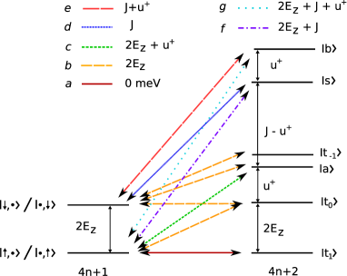
In the very same way it is possible to get trapped in the state via the state indicated by line c.
V.3 The magnetic field sweep
In a seminal experiment Moriyama et al.Mor1 demonstrated a transition from a groundstate to a groundstate upon magnetic field sweep in a SWNT quantum dot. In this section we have computed the differential conductance in a gate-voltage and magnetic field plot both for unpolarized, as in Mor1 , and parallel polarized leads with .
We start from the groundstate at with a band-mismatch of (smaller than we previously used). This choice yields a change of groundstate from to the triplet at a magnetic field T as measured experimentallyMor1 . To observe well visible patterns, we increased the temperature by a factor of ten compared to Tab. 2.
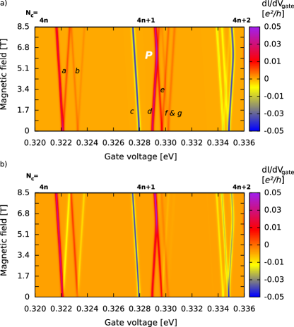
The result of our calculation is presented in Fig. 15a). At a gate voltage of approximately and we have two -shaped transition patterns (a and b) each of width . The separation between and at zero field is the band-mismatch . Interestingly, for polarized leads, the branches belonging to transitions involving , corresponding to the positive slope of the , are NDC lines, Fig. 15b). The reason is the same as addressed already in section V.2: once the - channel becomes available, there is some chance that from time to time a minority charge carrier ( - electron) enters from the source. As the drain is polarized in parallel to the source, it will take quite a while until this electron can leave the SWNT again, such that transport gets hindered. At the gate voltage of approximately , one enters the Coulomb diamond (line c) and transport gets completely suppressed. The dot is in the groundstate at . At transport from to the state is enabled (line d).
The next transitions (patterns e, f, g) we observe are again split by and therefore shaped like a ””. In all cases, the positively sloped branches are now again of NDC nature for a parallel lead polarization. The first ”” belongs to the triplet (pattern e) and is of stronger intensity than the following two patterns. The transitions and contribute to the negative sloped part, while and are responsible for the positive shaped line. The crossing of the and lines occurring at , point , indicates the change in the groundstate from to the state .
From the triplet pattern e the additional gate voltage equal to the exchange energy is needed to arrive at the last two ”” - shaped patterns and . Compared to the lines for the triplet transition they are quite close to each other and of less intensity. These lines belong to a transition from both the and the states to the - singlet (pattern f) and the state (pattern g). Finally, the lines on the right edges of the plots are mirror images and belong to backward transitions from to ; for this reason they mark a decrease of current for both polarized and unpolarized leads.
VI Conclusions
In summary, we have calculated spin dependent transport through fully interacting SWNTs in both the linear and the nonlinear regime, with and without an applied magnetic field.
Peculiar of metallic SWNTs of small diameter is the possibility, due to exchange interactions, to find the system at filling either in a groundstate of total spin or . Which of the two groundstates occurs in a real nanotube depends on the relation between the exchange energy and the orbital band mismatch. Thus, with focus on transitions involving filling, we investigated both situtations and demonstrated pronounced differences in the current-voltage characteristics depending on the considered groundstate.
For example in the linear regime the conductance for parallel lead magnetization and finite magnetic field increases by raising the polarization for the case of a triplet groundstate but it decreases for the groundstate. This is due to the fact that for the triplet groundstate transport is dominated by a channel involving the triplet state (with both spins ); for the case transport to be mediated by the majority electrons requires to make use of the lowest excited state (and hence less favorable), Zeeman split from the ground state.
In the nonlinear regime we presented stability diagrams with parallel and antiparallel lead magnetization for both ground sates. In the antiparallel case it was possible to observe a negative differential conductance (NDC) effect for the groundstate, following immediately upon a conductance enhancement at the opening of a trapping channel to the excited triplet state . Directly at that resonance, electrons can, just by thermal activation, tunnel back and fourth, such that trapping in the state can not yet act, leading to an intermediate conductance increase. Away from resonance, the blocking effect fully occurs, resulting in the NDC. By adding an external magnetic field in the parallel setup we found NDC effects for both groundstates caused by spin blocking mediated by - channels, involving in particular the triplet state .
Finally, we also presented results for the differential conductance in a gate-voltage and magnetic field map at finite bias. These magnetic field sweeps immediately allow to recognize the nature of the -filling groundstate at zero field, as well as to tune the nature of the groundstate from to upon variation in the field amplitude. Our results for unpolarized leads are in quantitative agreement with experiments on a small-diameter SWNT by Moryama et al. Mor1 . Importantly the sweep at zero field also allows to immediately read off the values of the short range interactions and . Specifically, is the singlet-triplet exchange splitting and characterizes at zero orbital mismatch the energy difference between two of the low energy states of total spin . In the presence of polarized leads the magnetic field sweep also reveals lines of NDC due to the trapping nature of all - channels.
The predictions of our theory are in quantitative agreement with experimental results obtained so far for unpolarized leads Mor1 ; Sap ; Liang . Due to recent achievements on spin-polarized transport in SWNTs Sahoo ; Man ; Haupt , our predictions on spin-dependent transport are within the reach of present experiments.
VII acknowledgments
We acknowledge support by the DFG under the funding programs SFB 689, GRK 638.
References
- (1) S. Iijima and T. Ichihashi, Nature 363, 603 (1993).
- (2) R. Saito, G. Dresselhaus and M. Dresselhaus, Physical Properties of Carbon Nanotubes, (Imperial College Press, London 1998).
- (3) A. Loiseau et al., Understanding Carbon Nanotubes, Lecture Notes in Physics, (Springer, Berlin 2006).
- (4) R. Egger and A.O. Gogolin, Phys. Rev. Lett. 79, 5082 (1997).
- (5) A. A. Odintsov and H. Yoshioka, Phys. Rev. B 59, R10457 (1999).
- (6) Y. Oreg, K. Byczuk and B. I. Halperin, Phys. Rev. Lett. 85, 365 (2000).
- (7) L. Mayrhofer and M. Grifoni, Eur. Phys. J. B 63, 43 (2008).
- (8) S. Moriyama, T. Fuse, M. Suzuki, Y. Aoyagi and K. Ishibashi, Phys. Rev. Lett. 94, 186806 (2005).
- (9) S. Sapmaz et al., Phys. Rev. B 71, 153402 (2005).
- (10) W. Liang, M. Bockrath and H. Park, Phys. Rev. Lett. 88, 126801 (2002).
- (11) A. Cottet et al., Semicond. Sci. Technol. 21, S78 (2006).
- (12) S. Sahoo et al., Nat. Phys. 1, 99 (2005).
- (13) H. T. Man, I. J. W. Wever and A. F. Morpurgo Phys. Rev. B 73, 241401(R) (2006).
- (14) J.R. Hauptmann, J. Paaske and P. E. Lindelof, Nat. Phys. 4, 373 (2008).
- (15) L. Balents and R. Egger, Phys. Rev. Lett. 85, 3464 (2000).
- (16) C. S. Peça, L. Balents and K. J. Wiese Phys. Rev. B 68, 205423 (2003).
- (17) S. Koller, L. Mayrhofer and M. Grifoni, New J. Phys. 9, 348 (2007).
- (18) I. Weymann, J. Barnas and S Krompiewski, Phys. Rev. B 76, 155408 (2007).
- (19) I. Weymann, J. Barnas and S Krompiewski, Phys. Rev. B 78, 035422 (2008).
- (20) W. Barford, Electronic and Optical Properties of Conjugated Polymers, (Clarendon Press, Oxford 2005).
- (21) P. Fulde, Electron Correlations in Molecules and Solids, (Springer, Berlin-New York 1995).
- (22) L. Mayrhofer and M. Grifoni, Eur. Phys. J. B 56, 107 (2007).
- (23) H. Yoshioka and A.A. Odintsov, Phys. Rev. Lett. 82, 374 (1999).
- (24) V. V. Deshpande et al., Science 323, 106 (2009).
- (25) J. v. Delft and H. Schoeller, Ann. Phys. 7, 225 (1998).