The impact of classical electronics constraints on a solid-state logical qubit memory
Abstract
We describe a fault-tolerant memory for an error-corrected logical qubit based on silicon double quantum dot physical qubits. Our design accounts for constraints imposed by supporting classical electronics. A significant consequence of the constraints is to add error-prone idle steps for the physical qubits. Even using a schedule with provably minimum idle time, for our noise model and choice of error-correction code, we find that these additional idles negate any benefits of error correction. Using additional qubit operations, we can greatly suppress idle-induced errors, making error correction beneficial, provided the qubit operations achieve an error rate less than . We discuss other consequences of these constraints such as error-correction code choice and physical qubit operation speed. While our analysis is specific to this memory architecture, the methods we develop are general enough to apply to other architectures as well.
1 Introduction
Quantum information processing (QIP) promises a path towards resolving currently computationally-intractable problems [1]. However, quantum bits (qubits) used for storing quantum information are, unfortunately, much more susceptible to errors than classical bits. Realization of error-corrected quantum computation, therefore, represents a critical QIP engineering pursuit. A key concept in this pursuit is the redundant encoding of a logical qubit in the state of many physical qubits. This redundancy allows one to check for errors and correct them.
This paper presents a solid-state architecture for a single logical qubit memory that accounts for the constraints imposed by both classical electronics and the native quantum gate set—the available set of qubit transformations the solid-state system provides. Quantum-computing architectures have been considered previously, for example in ion traps [2] and solid-state [3, 4]. These analyses began the study of incorporating realistic implementation constraints. We extend these studies in the solid-state to include explicit electronic constraints, where we expect electronics integration to be easier and the least constrained. From this we have gained a number of critical architectural insights including guidance about error-correcting code choice and quantum gate speed and scheduling limitations.
The rest of this paper is structured as follows. Section 2 is a brief background on quantum computing. Section 3 describes the solid-state qubit implementation, its assumed constraints and assumptions about noise. Section 4 provides an introductory description of quantum error correction and specifics on the Bacon-Shor code. Section 5 describes an “enclosed” architecture for a fault-tolerant logical qubit that is matched to the solid-state qubit constraints, and describes classical electronics constraints for scheduling error correction operations within the logical qubit. Section 6 describes how we optimized the error-correction schedule subject to these constraints. Section 7 quantifies when it is beneficial to use this logical qubit with a given native gate set and schedule. Section 8 summarizes our results and concludes.
2 Quantum computing background
Every quantum computation can be expressed as a quantum circuit in which a sequence of elementary transformations called gates act on a collection of elementary parcels of information called qubits. To understand the basics of quantum computing, then, it suffices to understand what qubits and gates are and how they interact. For a more detailed treatment of quantum computation, we refer the reader to any of the growing number of textbooks on the subject, such as Ref. [1].
A qubit is formed out of two isolated quantum states (e.g., a ground and excited state of an atom). Mathematically, we represent a qubit’s two states by the vectors and , which we call computational basis states. A general single-qubit state is of the form , where and are polar and azimuthal angles in spherical coordinates; the set of possible single-qubit states forms what is called the Bloch sphere.
A single-qubit (coherent) gate can be expressed as a rotation of the Bloch sphere. Some special one-qubit gates that we will discuss are the bit-flip gate , phase-flip gate , and the Hadamard gate , which correspond to rotations by about the axes , and respectively. Instead of being thought of in terms of abstract rotations, these gates are probably best understood in terms of their action on computational basis states:
| (1) | ||||||||
| (2) |
Mostly we will be interested in the rotation gates and about the and directions by arbitrary angles ; conveniently the Hadamard gate can be expressed as the triple sequence of rotations about , then , then , or more succinctly, .
A measurement of a qubit in the computational basis, an operation we denote by , will transform an isolated qubit’s state to with probability or to with probability . More generally, a qubit can be correlated with other qubits and the outcome probabilities of measurements will reflect these correlations. Because transforms a qubit, we will sometimes also call this a one-qubit (incoherent) gate. In principle one can measure a qubit in any basis; such a measurement is equivalent to a rotation which takes the computational basis to that basis, followed by . For example, a measurement consisting of and is denoted , and can be thought of as performing a Hadamard gate followed by .
Given a one-qubit (coherent) gate , the two-qubit controlled- gate, denoted , is defined by
| (3) |
The only two-qubit controlled gates we will discuss are the the controlled-NOT gate and the controlled-phase gate . While many other two-qubit gates exist, the only other ones we consider are Pauli operators. The set of one-qubit Pauli operators are , , , and the identity gate . The set of two-qubit Pauli operators are the two-qubit gates that act as a one-qubit Pauli operator on each qubit. The reason these gates are interesting is that any noise process on one qubit can be expressed as a linear combination of one-qubit Pauli operators and every noise process on two qubits can be expressed as a linear combination of two- qubit Pauli operators. In Sec. 5, we will discuss a noise model in which gates are assumed to act ideally followed by a Pauli operator drawn at random.
A universal gate set is necessary to do arbitrary computations. It is well-known that there are certain sets of classical logic gates over which any Boolean function can be expressed. An example of such a universal gate basis is the set consisting of NAND and FANOUT. In an analogous way, there are quantum universal gate bases over which any multi-qubit transform can be efficiently approximated. An example is , sometimes called the standard gate basis. To perform quantum error-correction, though, one does not need a fully-universal gate basis. It suffices to use only Clifford circuits, namely those generated by the gates , , CNOT, and . Clifford circuits are also generated by the set , where and in this context represent deterministic gates that prepare the states and respectively.
3 Physical Qubit, Native Gate Set, and Noise Assumptions for Logical Qubit
The physical qubit for this logical qubit analysis is a two electron spin system. The two electron spins are confined within a silicon double quantum dot (Si DQD) and they form two distinct spin configurations, a singlet or triplet, with two distinct energies analogous to a ground and excited state. These two states form the qubit’s computational basis states and . A gate set for the DQDs in GaAs was proposed by Taylor et al. [5], which consists of , Table 1. For effecting quantum error-correction, only a finite subset of these gates are necessary, for example the set suffices. We define this set of gates as the Si DQD native gate set. In addition to these gates, qubits also experience the “identity gate” by sitting idle. The gate is a modified idle, explained below, that relies on additional gate pulses to suppress noise.
| Gate | Time | Failure Probability | Estimated Decay Time | Estimated Error | Dominant Noise Source (anticipated) |
|---|---|---|---|---|---|
| , prep | N/A | pulse error incomplete or non-adiabatic transition | |||
| s | charge fluctuations on | ||||
| s | charge fluctuations on | ||||
| s | charge fluctuations on | ||||
| s | charge fluctuations on | ||||
| CPHASE | s | charge fluctuations on | |||
| s | non-uniform -field no DD | ||||
| ms | time varying non-uniform -field uncompensated by DD |
The Si DQD structure is assumed to look analogous to the GaAs qubit described by Taylor et al., using the same metal routes and area to electrostatically define the dots, Fig. 1 , with one exception being a top metal gate, Fig. 1 . The reservoir of electrons, out of which the single electron spins are isolated with the depletion gates, are produced by the application of a positive bias on the metal of a standard metal-oxide- semiconductor stack, Fig. 1 , which draws electrons into the critical area. The GaAs qubit does not require this metal gate because the electron reservoir can be built-in. Figure 1 also shows the inclusion of conducting routes that form a charge sensor (left and right most gates), to measure the qubit state. A total of 17 conducting routes are needed per Si DQD qubit not all of which are shown in Fig. 1 . Routes not indicated in the figure are 4 ohmic contacts, 2 local inductor leads, the top gate, and 2 CPHASE enables.
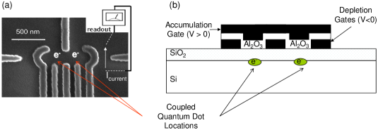
For the Si DQD qubit, we further modify the Taylor architecture in six key ways. We (1) identify the singlet, not the triplet, as the state; (2) model measurement, , as being much faster and more accurate, assuming a recently proposed integrated read-out approach [6]; (3) use measurement for rapid initialization of the state; (4) insert extra current pulses into the X-gate to negate effects of stray magnetic fields on neighbor qubits; (5) do not use physical qubit transport mechanisms despite being assumed available in the Taylor architecture; and (6) insert, in some instances as described later, dynamical decoupling pulses to achieve very low error memory, , compared to the bare memory . Several of the proposed modifications warrant further clarification. In the case of state preparation, error correction algorithms require the ability to prepare a qubit in a known state like the singlet, . The approach proposed for this logical qubit is to use measurement for state preparation by rapidly collapsing the state into a known or state rather than relying on triplet relaxation, to state, which is relatively slow. Although the error correction algorithm assumes a starting state, a measurement that yields a can be treated as a known error which can be accounted for later by classical feed-forward correction. Feed-forwarding is faster and less error-prone than correcting immediately with an X-gate. The extra current pulses proposed for the X-gate are used in conjunction with additional -gates to exchange the electron positions within the double quantum dot (DQD) qubit, this allows the application of an opposite polarity -field half way through the X-gate rotation. In this way, all neighbor qubits see a net zero rotation due to stray fields (assuming an identical but opposite -field pulse), while the target qubit sees the intended net X rotation. The challenges related to transport and our reasoning not to use it are explained later in this section.
A key contribution of this study is to examine the effect of electronics impact on the overall logical qubit performance. The details of the physical qubit and the native gate set define many of the requirements for the electronics. The effect of the native gate set and physical qubit on the electronics can be broken into its effect on three classic architectural design trade-off areas power, time, and space. Power constraints are very strict in the solid-state implementation because the DQD qubits must be cooled to 100 mK. Cooling to 100 mK requires specialized cryogenics (i.e., dilution refrigerators) that have very limited cooling powers especially at the 100 mK stage. This limits the amount of electronics that can be run on the 100 mK stage and forces most active (power consuming) electronics up to higher temperature stages, 4 K or 300 K, in the dilution refrigerator. Details regarding the choice of the staging of the electronics will be covered in Sec. 5.
Time of gates is impacted by the electronics through limits on timing precision (jitter), bandwidth between cryostat stages, and possibly cooling power (i.e., faster electronics dissipate more power). A clock period of 30 ns was used in this work. This clock period was chosen as a conservative estimate of what could be sustained with limited lines between stages, see Sec. 5, while assuring high timing precision for the gates (i.e., jitter). Scheduling constraints due to limits on the number of parallel operations are also discussed in Sec. 5.
The space required for the DQD qubit can have a severe affect on two dimensional lay-out at the 100 mK stage through the relationship of the qubit size and number of metal routes required for each qubit (i.e., 17 metal lines and ). One of the challenges related to space is that there is a limit to how many neighboring qubits can be placed in a row without overextending the number of possible metal lines available in that row for a given CMOS process, see Sec. 5. The logical qubit is, therefore, constrained to more of a quasi-1D lay-out, which was also previously noted by Szkopek et al. [7]. An important and weak assumption in this logical qubit is that each qubit is similar, which implies no additional tuning circuitry for individualized local tuning (tuning the DQD itself) or pulsing (tuning the pulse generators) is needed. We expect serious additional space and time penalties for tuning circuitry which is a topic for future work.
Transport of the physical qubit location can significantly relax space and time constraints. However, current proposals for transport (e.g., shuttling [8], and tunneling [9]) are even more speculative than the Si DQD and require additional hardware discovery. Logical transport of information can alternatively be done through qubit operations like teleportation [1] and SWAP (i.e., nearest neighbor exchange of qubit information without changing electron location). However, neither of these operations are provided in the native gate set, so realizing them would require additional nontrivial and error-prone gating. For example, the logical SWAP operation requires the translation of 3 CNOTs into the native gate set. We calculate that the relative error probability for a single SWAP operation using the DQD native gate set is 22 and it takes 16 steps to execute, which is to be compared to other gates in Table 1. The penalty for transporting by SWAP with this native gate set is, therefore, very high and undesirable.
Noise and error correction, as previously noted, are a dominant issue for quantum computations and are highly dependent on the choice of physical qubit and native gate set. In many cases, the effect of noise sources on a qubit can be characterized with an empirical time constant fit to an exponential decay in time [1]. The time constant can describe probability of errors such as spin flips, -like error, or dephasing (e.g., transversal decoherence). Most information about noise sources for electron spins in silicon comes from measurements of spin ensembles that are confined by donors [10]. These measurements indicate very low probabilities of spin flips and relatively slow transversal decoherence, denoted , of s–ms [10]. These decoherence times are considerably longer than those measured in GaAs, s [11], which is one of the primary motivations for studying Si qubits. The longer decoherence time in Si has been assigned to the ability to remove nuclear spin hyperfine coupling to the electron spin in isotope purified 28Si.
Additional gate pulses called dynamic decoupling pulses must be incorporated to achieve the reported long decoherence times in Si [12]. These pulses cancel noise from static non-uniform -field gradients over the entire sample. Without dynamical decoupling (DD), the decoherence times are anticipated to be s in silicon [13], which we use to infer the error probability of the gate in Table 1. In the case of the Si DQD qubit, a dynamic decoupling gate sequence of Z--Z- could be used similar to what was chosen for the GaAs qubit work [11]. is defined here as an arbitrary number, , of memory gates of 30 ns duration (i.e., ). A lower probability of memory error is used, for the case that dynamic decoupling is used and the decoherence time within the pulses is much slower, Table 1. For initial computational ease we used an X--X- schedule in this logical qubit analysis, which represents a worse case because errors are greater than errors.
Gate operations can expose qubits to further sources of noise. In particular the -gate uses an externally controllable exchange energy, , to rotate the qubit. The exchange energy is sensitive to the proximity of the two electrons, which is manipulated by external voltages that drive the electrons together or apart. The exchange energy is believed to be sensitive to charge fluctuations, which can alter the intended proximity and result in random rotation, which can rapidly dephase the qubit [14]. We model for the gate to be s, based on an assumed charge dephasing time of ns [15] and a sensitivity on local electrical potential of [14]. Because the interaction is also used to effect CPHASE gates and to implement our magnetic-field-canceling version of gates, this noise is present in those gates as well (Table 1).
Finally, we model the noise afflicting the and prep- gates as being much less severe than decoherence, motivated by a recent proposal for an integrated charge-sensing device [6]. Because this device is assumed to work quickly (faster than 30 ns) and with high sensitivity, we model the gate time and error rate of and to be and respectively. Recall that the gate which prepares is essentially identical to the gate; application of returns or , and if a was mistakenly obtained, it is merely recorded classically and managed with adaptive feed-forward correction, which appropriately re-interprets the meaning of the state.
4 Local Check Codes
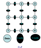
An architecture for which transport is costly or impossible motivates the use of local check codes. Local check codes are examples of what are known as stabilizer codes [1], which are characterized by a collection of check operators that fix or “stabilize” valid code states. Local check codes are also low-density parity-check (LDPC) codes, namely ones in which each qubit is involved in at most a constant number of check operators and each check operator acts on at most a constant number of qubits, which eases routing requirements. Local check codes have the additional property that the check operators are local relative to some qubit geometry, obviating the need for transport to measure them. So far only three general classes of local check codes are known: surface codes [16], color codes [17], and Bacon-Shor (BS) codes [18]. In this paper we focus on BS codes because they require the simplest error correction circuits of these three classes. Of these, we focus on the simplest BS code—the one which encodes one qubit into nine (arranged in a grid) that can correct for an arbitrary quantum error on a single qubit. This code, which we call BS9, is depicted in Fig. 3. For reasons explained in Sec. 5, larger codes on a square lattice are difficult to realize in our architecture because of transport and routing constraints.
BS9 quantum error correction is a two-phase process: syndrome extraction followed by error recovery. In BS9 syndrome extraction, one first measures the parity of every pair of horizontally-neighboring qubits—are they of even parity ( or ) or odd parity ( or )? Then one measures the parity of the phases of every pair of vertically-neighboring qubits—are they of even parity ( or ) or odd parity ( or )? Even if the neighboring qubits weren’t in a state of definite (bit or phase) parity before such a measurement, they are guaranteed to be so afterwards because the measurement of one of these “local parity checks” forces them to decide. The collection of outcomes of these measurements is called the syndrome because it “diagnoses” what, if any, errors have afflicted the encoded state.
There are 6 vertical parity checks and 6 horizontal parity checks that need to be made. For reasons having to do with operator theory in quantum mechanics, we call these and checks respectively. In principle, a single qubit can be re-used to store each of these measurements, with the result copied off to “classical” storage elsewhere between each re-use. A more local strategy is to place “ancilla” or “syndrome” qubits in between each pair of “data” qubits involved in a local check. Since this results in 9 + 12 = 21 qubits, we call this architecture the BS9 (21) architecture. The syndrome and data qubits are identified in Fig. 3.
The error recovery phase of BS9 error correction is a classical algorithm that processes the syndrome and makes a determination of what the most likely error is. Because errors can afflict not just the data but also the process of syndrome extraction itself, it is important to not be too reactionary to the observed syndrome. To be confident in the syndrome values, we could repeat the process three times and take the majority of the outcomes. However, it turns out to be sufficient (and better) to simply repeat once and if the two syndromes disagree, wait until the next cycle of error correction to catch the error. Because this method is resilient to faults in the syndrome extraction process itself, we call it fault-tolerant.
Once an error is identified by the error recovery phase, it need not be corrected immediately. It suffices to simply keep a log of the error and only apply the net correction when one wishes to extract information from the logical qubit. This removes the possibility that errors could accumulate during the correction steps that would be applied otherwise. We call this the feed-forward property of quantum error correction.
5 The Logical Qubit
Based on the BS9 error correction protocol, the native gate set, and physical qubit described in Section 3, an “enclosed” architecture, shown in Fig. 3, was created. The fully enclosed architecture was chosen to optimize the parallel access of the read-out and classical electronics to the interior qubits. This architecture provides a platform to probe the interactions between quantum hardware, quantum protocols, and classical electronics for which we attempt to minimize the impact of limitations imposed by the classical hardware.
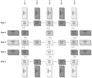
The architecture in Fig. 3 consists of quantum hardware (DQDs), and classical CMOS electronics. Each CMOS block controls signals to the DQDs shaded the same color in a particular row or column, the number of DQDs controlled by the CMOS block is shown in parentheses. The capacitor located between neighbor DQDs illustrates the electrical coupling needed to perform 2-qubit gate operations such as CPHASE . Coupling can be done on the left or right side of the DQD, so vertical coupling is labeled or if the coupling occurs on the right or left side of the DQDs, respectively.
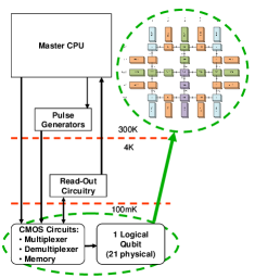
As described in Section 3, the choice of where each piece of the classical architecture is staged in a cryostat is an important question of trade-offs between speed, area, power dissipation, and local/global heating. Figure 5 shows the electronics staging design used in this analysis. The 300 K stage holds the master CPU responsible for classical and quantum protocol control as well as the pulse generators used to generate the pulse sequences to gate the DQDs located at 100 mK. The pulse generators could be moved to lower temperature stages, dependent on their power dissipation, but for simplicity were not in this exercise. The 4 K stage holds the circuitry used to readout the state of the DQDs. The read-out circuitry consists of a single electron charge sensor, located at 100 mK, connected to an integrated comparator and latch, located at 4 K. The read-out is placed at a cooling stage close to the 100 mK stage to minimize RC delay. The 100 mK stage holds the DQDs and supporting classical CMOS electronics. The CMOS blocks at 100 mK contain multiplexers (MUX) for routing the pulse signals from 300 K to each DQD, and demultiplexers (DEMUX) for reading-out the state of the DQDs (Fig. 5). Additional circuitry not shown includes the memory used to hold the state of the MUX/DEMUX during operation.
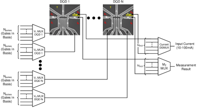
There is a limit on the number of parallel signal lines that can be run from the higher temperature stages to the 100 mK stage, which limits bandwidth and parallelization. The limitation is a result of control lines between stages consuming area and also introducing additional heating paths between temperatures stages. This concern makes it desirable to use the smallest number of connections as possible while maintaining a minimal bandwidth penalty. One way to achieve this is to send the control information serially between the 300 K stage and the 100 mK stage.
We can analyze the number of serial lines needed to control the MUX/DEMUXs for a given number of DQDs based on the following assumptions (Fig. 5): (1) Control lines are used to set-up the MUXs and DEMUXs at 100 mK; (2) 8 control bits are needed per DQD for this architecture; 3 bits to setup the Right Control MUX, 3 Bits to setup the Left Control MUX, 1 Bit for Measurement MUX, and 1 Bit for controlling the inductor current. Note the required number of control bits is a function of the number of gates in our native gate set. (3) A time step is defined as the fastest qubit gate and takes multiple serial clocks; (4) Control bits are pipelined. Information being sent serially during time step “” is used during time step “” and all information must be sent before the next time step.
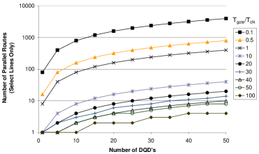
The number of control lines as a function of qubits in the quantum circuit is calculated for several different gate to serial clock ratios, (Fig. 6). A ratio of less than one implies the gate time is faster than the clock period, this does not apply to our architecture but is included for completeness. Typical cryostat’s have less than 100 interconnects between 100 mK and 4 K. Several trends are highlighted by this calculation including a rapid and unsustainable number of lines necessary to achieve low ratios of Tgate/Tclock.
The wire length between qubits is assumed to be as small as possible to minimize parasitic capacitive links to other routing lines. Unintentional voltage variations due to cross-talk through parasitic capacitance’s would lead to unintentional qubit rotations, this is minimized with short coupling wires between the qubits for CPHASE . For these reasons this analysis assumes that the physical qubits must be placed very close to one another and the distance for this analysis is 250 nm.
The classical electronics on the 100 mK stage that services the qubits (i.e., MUX-DEMUX and memory) requires non-negligible space and must be commensurate to the physical qubit spacing, the width of the metal lines, and the available levels of metal routing. The number of metal levels is limited by currently available technologies. This imposes a constraint on the number of routing channels available along a single linear span of DQD qubits, Fig. 3 (i.e., shaded grouping). Because a minimum wire length between qubits is assumed, the CMOS blocks have a fixed width available to extend metal routes to service each of the DQDs. By fixing the width of the CMOS block we are also fixing the number of channels available to route into the enclosed architecture along a single span which affects the total number of DQDs accessible by a CMOS block. The total number of DQDs that can be reached for different technology nodes (i.e., metal widths) based on the number of shared or common signals among DQD is calculated in Table 2 (10 nm and 1 nm nodes are fictional). For this calculation the architecture assumes that: (1) signals are only brought from one side of the DQD, (2) the DQD qubit is , (3) DQDs are placed 250 nm apart, (4) each DQD has 17 control lines.
| Technology | 130 nm | 90 nm | 65 nm | 10 nm | 1 nm |
|---|---|---|---|---|---|
| Routes per m | 19 | 27 | 40 | 462 | 4662 |
| Accessible DQD (No Common Signal) | 1 | 1 | 2 | 30 | 308 |
| Accessible DQD (5 Common Signals) | 1 | 2 | 3 | 42 | 436 |
The number of accessible qubits is very limited even when considering relatively advanced CMOS nodes such as 65 nm. This estimate, furthermore, does not account for a reduction of available paths due to cross talk concerns related to running signals directly over DQDs. It is unclear whether these paths can be tolerated. Techniques exist to reduce cross-talk such as additional ground planes, but this also has not been considered in this analysis, and will likely further decrease the number of DQDs accessible by a CMOS block. The routing limitations highlight the importance of space saving approaches such as sharing signal lines between DQDs as well as developing more flexible lay-outs that provide larger spacing between DQDs or larger DQD blocks. For the enclosed architecture we assume 5 common signals (Table 2), which makes it conceivable to reach 3 DQDs with one CMOS block while still using a non-fictional technology node (e.g., 65 nm). The impact of spacing flexibility relative to increasing the number of accessible qubits provides a strong motivation for development of physical qubit transport methods that do not require a high density of metal routes.
Constraints on the quantum circuit scheduling begin to emerge from these considerations of space and 300 K to 100 mK bandwidth. One goal of this work was to establish the impact of the electronics architecture on the quantum circuit performance. One form in which the electronics impact manifests itself on the performance is through establishing constraints on the QEC code schedule. Using the enclosed architecture as described above combined with the assumptions in Table 3, a list of constraints was created and is presented in Table 4.
| Assumption | |
|---|---|
| 1 | Fastest gate will be 30 ns for a rotation |
| 2 | All DQDs are similar and tuning is not required. |
| 3 | 5 leads can be shared among DQDs (). |
| 4 | Pulses can be applied in parallel to multiple DQDs. |
| 5 | Serial clock is operating at 1 GHz |
| 6 | Gate pulses have the required precision to meet the error rates in 1. |
| 7 | 1 Pulse Generator exists for each gate of Table 1. CPHASE requires 3 pulse generators. |
| Constraint | |
|---|---|
| 1 | Active control signals can only be passed over DQDs (CPHASE between neighbors is acceptable). This reduces effects of cross-talk. |
| 2 | The same single qubit gate can be applied to any number of DQDs controlled by a CMOS block. Single qubit gates of differing types are not allowed. |
| 3 | One measurement can be done per CMOS block |
| 4 | CPHASE gate can be applied to DQDs not controlled by the same CMOS block. |
| 5 | CMOS blocks controlling multiple DQDs can perform CPHASE gates in parallel if the direction of coupling between DQDs is appropriate. Example: CPHASE (Col3Row3, Col3Row4) & CPHASE (Col2Row5, Col3Row5) is acceptable but CPHASE (Col3Row3, Col3Row4) & CPHASE (Col3Row5, Col4Row5) is not. |
6 Computing an Optimal Error Correction Schedule
In this section, we describe the integer program (IP) used to compute the optimal schedule for a quantum memory using the BS9 architecture described in Section 5 and shown in Figs. 3, 3, and 5. Due to space limits, we summarize the nature of the formulation and computational considerations but do not give a formal mathematical formulation.
We assume time is divided into “ticks” that represent the minimum time step for the shortest functional gates (I, , , prep , ). All longer gates’ running times are rounded to integral multiples of this tick size. Thus each operation requires a small number of ticks. We use a time-indexed formulation. This allows binary decision variables and generally provides a tighter linear-programming relaxation, both important for practical solver performance. However, the size of the formulation (number of variables and constraints) depends upon an upper bound for the schedule length, or makespan.
Our goal is to determine a legal start tick for each operation (row and/or column circuit operation) for each qubit. For data qubits, row/column operations cannot interleave except that -type operations at the boundary between row and column operations ( & CPHASE ) can commute. Thus, we must always obey a series of precedence constraints within each circuit, and we must obey precedence constraints conditionally based on circuit ordering decisions for each data qubit. Qubits may be idle at any given tick. All qubits that share a controller must perform the operation the controller is signaling, and execute without interruption.
We wish to schedule all the circuits subject to the constraints (Table 4) to minimize the total idle time of all qubits. Holding qubits in memory contributes to qubit errors. The data qubits are in continuous (re)use, so their idle time is determined by the makespan. Specifically, for data qubit , the idle time is the makespan minus the total time to execute the gates for . The gate execution time depends upon the number of CPHASE gates, which is determined by the qubit’s physical position within its row and column circuits. Idle time for ancilla is the total number of idle ticks between preparation and measurement.
Because operation placement and controller decision variables are indexed by a tick, we must know a valid upper bound on the makespan of an optimal schedule. This determines the number of variables. Specifically the number of variables grows linearly with the schedule length. Perhaps more important than the size of the formulation, the flexibility (number of schedules) increases dramatically with makespan, and thus solver time also increases rapidly. It is generally worthwhile to find a good upper bound, for example from a valid hand-generated or heuristically-generated schedule, rather than using a naive bound such as the length of a serial schedule.
We began by solving a version of the problem that minimizes makespan, finding the minimum number of ticks to legally complete the schedule, rather than the minimum total idle time. We set the initial makespan guess from the length of a hand-generated schedule. By maximizing the number of ticks where controllers are completely idle at the end of the schedule, we can compute a minimum makespan. We then used the minimum makespan as the first estimate for the makespan when computing a minimum-idle-time schedule. This objective explicitly trades off makespan vs. ancilla idle time. The optimal schedule for this makespan had only two total idle ticks summed over all ancilla. Because increasing the makespan would add ticks of idle time taken over all the data bits, while possibly only remove ticks from the ancilla, this schedule is optimal over all makespans.
For practical performance, we computed tight legal time windows on all the operation variables and a reasonable lower bound on the makespan. We ran the IP using the ampl mathematical programming language and the cplex 11.0 integer programming solver on a dual-core 32-bit linux workstation with 3.06Ghz Xeon processors with 2Gb of RAM. The final problem, to compute the minimum idle time knowing the optimal makespan solved in less than a second. The problem ampl sent to the solver after preprocessing had 4701 binary variables, 5784 constraints, and 58163 nonzeros. The IP computed an optimal schedule that had 95 idle ticks, which is a significant improvement from a hand-generated schedule with 129 idle ticks.
Adding DD requires significant changes. We enumerate the possible DD blocks for each qubit, built from a set of maximal DD blocks. We require the IP to select precisely one DD block containing any operation that requires DD. For data qubits, each tick must be inside a DD block. Idle time at the end of the “wait” interval of the last block can wrap around to cover idle time at the start of the schedule. The controller must signal the -gates used for DD as appropriate given the block starting time. We constrain the operations to run during the appropriate “wait” interval for their DD block. We allow the previous constraints to enforce precedence and all other operation constraints. Computing optimal DD-based schedules for Z--Z- refocusing is future work.
7 BS9 Threshold Calculations
In order to assess the performance of any logical qubit architecture, we need an explicit noise model. Here we consider the depolarized noise (DPN) model in which each gate other than measurement is chosen to work flawlessly with probability or else be followed by one of the non-identity Pauli operators selected uniformly at random. Sometimes we will consider a variant of this noise model, the biased DPN model, in which certain gates are more or less likely to fail than others. We generally draw the relative error probabilities for the biased DPN model from Table 1 in Sec. 3 to model classical electronics constraints, although sometimes we tweak this biasing to study the relative importance of certain gates’ fault rates. While we estimate for realistic gates in Table 1, we consider more general DPN models in this section in which is variable. We note that in both noise models, in addition to measurements, the identity gate (representing idling qubits) will have a fault probability different from the rest of the gates. Furthermore the failure probability of the identity gate will be a constant and will depend on whether or not DD is used during error correction. This is done to maintain consistency with our hardware characteristics described in Section 3.
The accuracy threshold is a figure of merit for a logical qubit architecture
realizing arbitrary computation [19]. In this work we are not
interested in arbitrary computation, rather just the creation of a logical
qubit memory. Consequently we define a figure of merit called the error threshold that
is closely related to the accuracy threshold, but is more relevant to our work.
Assume the noise in the error correction circuit is DPN with failure probability
, then the probability of failure for error correction [] is an
increasing function of .
Approximate Definition: The error threshold for a DPN model is
the maximum failure probability for which .
The accuracy threshold is defined in a similar way with the maximum failure
probability of the logical gate set replacing () in the above
definition. In our work there is only one logical gate, namely the logical
identity with failure probability . However, there is a problem with
the above definition in our context. The identity gate in our error
correction circuit has a constant failure probability () and as such
. Hence, there is no that satisfies the above definition.
We want to highlight this nature of , since it is significantly
different from the fault tolerant logical gate failure probabilities for
distance-3 codes [19] that behave like . We reiterate that
this difference is due to the fact that the idle periods in our architecture
have a fixed non-zero error probability. With this in mind and allowing for
a biased DPN we define:
Definition: The error threshold for a (biased) DPN model is the
maximum failure probability for which there exists an
such that , where
is the maximum probability of failure of the native gate (NG) set. Note that
for DPN and for the biased DPN from Table 1.
The intuition behind the above definition is the following. Error
correction is realized using the native gate set while accounting for
hardware constraints. The error threshold is the failure probability that the native
gates need to perform better than in order for the error correction failure probability to
be lower (better) than the worst individual gate used in the error correction.
We note that in the context of designing for a logical qubit, one could also define an
error threshold based on memory. In other words, assuming a noise model like DPN,
one could ask for the input error probability such that the failure rate of
error correction is lower (better) than the failure rate of an idle. Here
failure rate implies the failure probability is normalized by the time
taken for the ”gate”. In view of space limitations we do not present our
work in this context.
A threshold only exists when syndrome extraction is processed fault-tolerantly, such as via the “repeat twice” syndrome measurement strategy we suggested in Sec. 4, or more generic strategies such as the ones proposed by Shor [20], Steane [21] and Knill [22]. Regardless of which fault-tolerant syndrome extraction strategy one uses, there is a well-developed, but technical method using “extended rectangles” (EX-REC) [19] that allows one to estimate the threshold of any architecture.
Using the EX-REC method, we computed the error threshold using Monte Carlo techniques for the BS9 (21) code for the following settings, each one becoming increasingly closer to describing an architecture constrained by the limitations of classical electronics:
-
1.
Syndrome measurements are not modeled as circuits but rather as “black box” processes that either occur ideally or suffer a fault according to a DPN model.
-
2.
Syndrome measurements are effected by circuits subject to a DPN model that implement Steane’s fault-tolerant protocol [21], where these circuits are expressed over the (nonlocal) gate basis .
-
3.
Syndrome measurements are effected by IP-optimized circuits described in Sec. 6, constrained by the classical electronics requirements listed in Sec. 5, implementing the “measure twice” fault-tolerant protocol described in Sec. 4 over the Si DQD native gate basis described in Sec. 3. Computing the error threshold in this setting is one of the main goals of this paper. Both the biased and unbiased DPN models are considered. The entire analysis is done for both the situations in which () there is no DD and with a provably optimum schedule for minimizing idles () there is DD without an optimal schedule. The change in error correction using DD from the no DD case is that there are additional and gates, but the failure probability of the identity drops from to .
To perform Monte Carlo studies of the error threshold for these settings, we used a self-modified extension of the QDNS simulator [23] to input an EX-REC for the error correction circuit of the desired form for the BS9 (21) code. We then fed this circuit into a message-passing-interface parallelized Monte Carlo simulator we developed that estimates the failure probability of the error correction circuit [] in the DPN and biased DPN models. Finally, we computed the error threshold using a bisection search to determine the crossover point, i.e., when for DPN and for the biased DPN models. The results of our Monte Carlo studies are presented in Table 5.
| Black box | Steane | NG & Opt. Sched. | NG, DD, Sub-Opt. Sched. | |
|---|---|---|---|---|
| unbiased | No Threshold | |||
| biased | No Threshold |
Several trends can be extracted from this table. To begin, the threshold is very high in the “black-box” model, reflecting the fact that this model just probes the quantum error-correction code’s ability to correct data errors independent of the architecture surrounding it. The case examines precisely this; the case is motivated by the fact that only and errors cause an measurement to fail where a error does not. The Steane model results show that gate errors in the syndrome extraction can contribute much more to the threshold than data errors during idles, causing a drop in the threshold by a factor of more than 10 even when idles are error free (). In part, this is an artifact of the nonlocal gates in the Steane circuit which can be parallelized to such a degree that they hardly leave data qubits idle at all. The NG model shows the large penalty incurred in changing the circuitry to accommodate classical electronics constraints faced by a Si DQD architecture. Even with an optimal schedule to minimize the number of idles we find there is no threshold. This is due to the large number of idles in the NG model (Table 6) whose error rates are significantly high (), resulting in . In other words, even if the native gate set is error free the error correction has a failure probability of 0.4. However, when we incorporate DD into the error correction we vastly improve the situation and actually obtain an error threshold. This is because although DD increases the number of and gates in the error correction, which would lead one to assume increases , it more than compensates for this by decreasing by a factor of . This suggests that under the current hardware assumptions for our architecture, DD is essential. Finally, while the error threshold for biased DPN is lower than the error threshold for unbiased DPN, it is not significantly smaller and in fact may even be more achievable. This is because the biased DPN allows some gates to be less reliable than others; for example, the error threshold for the biased DPN requires that , , and CPHASE gates err with probability below , which is a higher probability than than the error threshold demanded for these gates by the unbiased DPN.
| Gate | BS9(21) w/o DD | BS9(21) with DD |
|---|---|---|
| of Gates | of Gates | |
| Prep | 12 | 12 |
| 42 | 42 | |
| 18 | 18 | |
| 0 | 104 | |
| CPHASE | 24 | 24 |
| 12 | 12 | |
| / | 95 | 219 |
8 Conclusion
This paper describes a solid-state error-corrected logical qubit memory that accounts for constraints imposed by both electronics and the native gate set. The combination of physical qubit geometry, electronics layout, and lack of a viable transport mechanism forces a restricted qubit layout and positioning of supporting electronics. We chose the Bacon-Shor code, a local check code, to accommodate the transport constraint. We also observe that limits on space for metal routing, even for the 65 nm CMOS process nodes, result in a maximum reach of three DQDs per CMOS block. This drove us to consider the smallest Bacon-Shor code that can correct for a single-qubit error, the BS9 code.
We developed a fault-tolerant procedure for carrying out error-correction with the BS9 code for our memory architecture, including a schedule for the native gate set that was constrained by limits of the electronics. We constructed rules for limits on simultaneous parallel gate operations and gate time to reflect concerns regarding cross-talk and signal bandwidth limits between cryostat stages. The electronics scheduling constraints lead to extra idle time penalties. We created a general IP methodology for minimizing idles in error-correction subject to the hardware constraints.
We developed a figure of merit relevant for our architecture that we call the error threshold that closely resembles the accuracy threshold for fault-tolerant quantum memory in the literature. Using this figure of merit and a 30 ns clock period, which leads to very error-prone idles, we find that our architecture has no error threshold, even with a provably-optimal schedule.
The idle error probability can be suppressed dramatically with dynamical decoupling (DD) pulses. Using -Idle--Idle DD and a hand-generated non-optimal error-correction schedule, we found that even with a 30 ns clock period, our architecture achieved an error threshold of for a depolarized noise model and for a biased noise model. This highlights the importance of combining multiple error-suppression strategies when classical electronics constraints are considered. We also find that these threshold values are a factor of approximately twenty larger than more abstract architectures. This is principally because of the extra 104 gates required for DD during error correction. Additional idles are also added to the schedule due to DD, but DD significantly reduces the impact of these idles.
In summary, we examined a hypothetical solid-state logical qubit memory architecture constrained by more realistic electronics and native gate set constraints. Layout constraints motivate a local error correction code choice. Electronics constraints on scheduling manifest themselves as a penalty due to additional idle times, which in turn requires additional gating and DD to suppress idle noise. We calculated optimal schedules and an error threshold for this more realistic case. We note that although this analysis was specific to a silicon solid-state implementation and quantum memory, the insight and tools developed apply more generally, especially to other implementations that are intended to operate in cryostats with CMOS electronics control and read-out.
References
- Nielsen and Chuang [2000] M. A. Nielsen and I. L. Chuang, Quantum Computation and Quantum Information (Cambridge University Press, Cambridge, 2000), ISBN 0-521-63235-8 (Hardback), 0-521-63503-9 (Paperback).
- Balensiefer et al. [2005] S. Balensiefer, L. Kregor-Stickles, and M. Oskin, An evaluation framework and instruction set architecture for ion-trap based quantum micro-architectures, in Proceedings of the 32nd International Symposium on Computer Architecture, IEEE (IEEE Press, Los Alamitos, 4–8 Jun., 2005, Madison, WI, USA, 2005), pp. 186–196, doi:10.1109/ISCA.2005.10.
- Loss and DiVinzenzo [1998] D. Loss and D. P. DiVinzenzo, Quantum computation with quantum dots, Phys. Rev. A 57, 120 (1998), doi:10.1103/PhysRevA.57.120, arXiv:cond-mat/9701055.
- Hollenberg et al. [2006] L. C. L. Hollenberg, A. D. Greentree, A. G. Fowler, and C. J. Wellard, Two-dimensional architectures for donor-based quantum computing, Phys. Rev. B 74, 045311 (2006), doi:10.1103/PhysRevB.74.045311, arXiv:quant-ph/0506198.
- Taylor et al. [2005] J. M. Taylor, H.-A. Engel, W. Dür, A. Yacoby, C. M. Marcus, P. Zoller, and M. D. Lukin, Fault-tolerant architecture for quantum computation using electrically controlled semiconductor spins, Nature Physics 1, 177 (2005), doi:10.1038/nphys174.
- Gurrieri et al. [2008] T. M. Gurrieri, M. S. Carroll, M. P. Lillly, and J. E. Levy, CMOS integrated single electron transistor electrometry (CMOS-SET) circuitry for nanosecond quantum-bit read-out, in Proceedings of the 8th IEEE Conference on Nanotechnology, IEEE (IEEE Press, New York, 18–21 Aug. 2008, Arlington, TX, USA, 2008), pp. 609–612, doi:10.1109/NANO.2008.183.
- Szkopek et al. [2006] T. Szkopek, P. Boykin, H. Fan, V. Roychowdhury, E. Yablonovitch, G. Simms, M. Gyure, and B. Fong, Threshold error penalty for fault-tolerant quantum computation with nearest neighbor communication, IEEE Trans. Nanotech. 5, 42 (2006), doi:10.1109/TNANO.2005.861402, arXiv:quant-ph/0411111.
- Fujiwara and Takahashi [200l] A. Fujiwara and Y. Takahashi, Manipulation of elementary charge in a silicon charge-coupled device, Nature 410, 560 (200l), doi:10.1038/35069023.
- Switkes et al. [1999] M. Switkes, C. M. Marcus, K. Campman, and A. C. Gossard, An adiabatic quantum electron pump, Science 283, 1905 (1999), doi:10.1126/science.283.5409.1905, arXiv:cond-mat/9904238.
- Tyryshkin et al. [2003] A. M. Tyryshkin, S. A. Lyon, A. V. Astashkin, and A. M. Raitsimring, Electron spin relaxation times of phosphorus donors in silicon, Phys. Rev. B 68, 193207 (2003), doi:10.1103/PhysRevB.68.193207, arXiv:cond-mat/0303006.
- Petta et al. [2005] J. R. Petta, A. C. Johnson, J. M. Taylor, E. A. Laird, A. Yacoby, M. D. Lukin, C. M. Marcus, M. P. Hanson, and A. C. Gossard, Coherent manipulation of coupled electron spins in semiconductor quantum dots, Science 309, 2180 (2005), doi:10.1126/science.1116955.
- Khodjasteh and Lidar [2005] K. Khodjasteh and D. A. Lidar, Fault-tolerant quantum dynamical decoupling, Phys. Rev. Lett. 95, 180501 (2005), doi:10.1103/PhysRevLett.95.180501, arXiv:quant-ph/0408128.
- Lyon [2008] S. A. Lyon, (private communication) (2008).
- Hu and Sarma [2006] X. Hu and S. D. Sarma, Charge-fluctuation-induced dephasing of exchange-coupled spin qubits, Phys. Rev. Lett. 96, 100501 (2006), doi:10.1103/PhysRevLett.96.100501, arXiv:cond-mat/0507725.
- Gorman et al. [2005] J. Gorman, D. G. Hasko, and D. A. Williams, Charge-qubit operation of an isolated double quantum dot, Phys. Rev. Lett. 95, 090502 (2005), doi:10.1103/PhysRevLett.95.090502, arXiv:cond-mat/0504451.
- Kitaev [2003] A. Y. Kitaev, Fault-tolerant quantum computation by anyons, Ann. Phys. 303, 2 (2003), doi:10.1016/S0003-4916(02)00018-0, arXiv:quant-ph/9707021.
- Bombin and Martin-Delgado [2006] H. Bombin and M. A. Martin-Delgado, Topological quantum distillation, Phys. Rev. Lett. p. 180501 (2006), doi:10.1103/PhysRevLett.97.180501, arXiv:quant-ph/0605138.
- Bacon [2006] D. Bacon, Operator quantum error-correcting subsystems for self-correcting quantum memories, Phys. Rev. A 73, 012340 (2006), doi:10.1103/PhysRevA.73.012340, arXiv:quant-ph/0506023v4.
- Aliferis et al. [2006] P. Aliferis, D. Gottesman, and J. Preskill, Quantum accuracy threshold for concatenated distance-3 codes, Quant. Inf. Comput. 6, 97 (2006), arXiv:quant-ph/0504218.
- Shor [1996] P. W. Shor, Fault-tolerant quantum computation, in Proceedings of the 37th Annual Symposium on Foundations of Computer Science, edited by R. S. Sipple, IEEE (IEEE Press, Los Alamitos, CA, 14–16 Oct. 1996, Burlington, VT, USA, 1996), pp. 56–65, ISBN 0-8186-7594-2, arXiv:quant-ph/9605011.
- Steane [1997] A. M. Steane, Active stabilization, quantum computation, and quantum state synthesis, Phys. Rev. Lett. 78, 2252 (1997), doi:10.1103/PhysRevLett.78.2252, arXiv:quant-ph/9611027.
- Knill [2005] E. Knill, Quantum computing with realistically noisy devices, Nature 434, 39 (2005), doi:10.1038/nature03350, arXiv:quant-ph/0410199.
- Imre et al. [2004] S. Imre, P. Abrontits, and D. Darabos, Quantum designer and network simulator, in Proceedings of the First Conference on Computing Frontiers (ACM Press, New York, 14–16 April 2004, Ischia, IT, 2004), pp. 89–95, ISBN 1-58113-741-9, doi:10.1145/977091.977106.