Pb chains on reconstructed Si(335) surface
Abstract
The structural and electronic properties of Si(335)-Au surface decorated with Pb atoms are studied by means of density-functional theory. The resulting structural model features Pb atoms bonded to neighboring Si and Au surface atoms, forming monoatomic chain located 0.2 nm above the surface. The presence of Pb chain leads to a strong rebonding of Si atoms at the step edge. The fact that Pb atoms occupy positions in the middle of terrace is consistent with STM data, and also confirmed by simulated STM images. The calculated band structure clearly shows one-dimensional metallic character. The calculated electronic bands remain in very good agreement with photoemission data.
pacs:
73.20.At, 71.15.Mb, 79.60.Jv, 68.35.B-, 68.47.FgI Introduction
One-dimensional (1D) atomic chains created on semiconductor templates have recently attracted much attention due to new phenomena characteristic for a reduced dimensionality Giamarchi . The most spectacular examples include a breakdown of Fermi liquid theory Luttinger ; Auslaender and Peierls metal-insulator transition Peierls . A specially attractive route to create such 1D structures is a process of self-organization of atoms into very regular arrays of parallel metallic chains on stepped semiconducting or insulating substrates Himpsel ; Owen . In this case electrons near the Fermi energy are completely decoupled from the substrate due to band gap in electronic spectrum of the substrate. The chain atoms are bounded to the surface by low energy states which do not contribute to electronic properties of the system.
The Si(335)-Au surface is one of the simplest examples of high-index surfaces which stabilize the one-dimensional structures, and has been studied by number of techniques, including: reflection high energy electron diffraction (RHEED) Zdyb , scanning tunneling microscopy (STM) Crain ; MK_1 , angle-resolved photoemission spectroscopy (ARPES) Crain ; Kisiel and first principles density functional theory (DFT) MK_2 . In particular, the STM topography data show regular arrays of monoatomic chains separated by width of Si(335) terrace and a few nanometers long Crain ; MK_1 . The ARPES spectra taken in the direction parallel to the steps show two highly dispersive bands crossing the Fermi energy (), thus indicating one-dimensional metallic nature of the system Crain . The structural model of the Si(335)-Au surface has also been proposed Crain and confirmed later by the DFT calculations MK_2 , which well describes all the available experimental data.
Recently, other materials (Na, Pb, In) deposited on Au decorated Si(335) surface have also been studied Starowicz ; Jalochowski ; Kisiel_2 ; Zdyb_2 ; Skrobas ; Zdyb_3 . Perhaps lead is the most intensively studied among them. Unlike Si(335)-Au surface, in which gold substitutes Si atoms in the surface layer, the Si(335)-Au/Pb is a representative of new class of systems in which the deposited material forms one-dimensional structures adsorbed on-top of the surface. The lead deposited on flat Si(111)-Au(66) surface forms well ordered monoatomic layers Jalochowski_2 ; Jalochowski_3 ; Jalochowski_4 , and is known to weakly interact with the Si substrate Dil . Thus, in the case of Si(335)-Au/Pb structure, one can expect a more pronounced one-dimensional character of chains as compared to clean Si(335)-Au reconstruction. Indeed, the deposition of 0.28 ML of Pb on reconstructed Si(335) surface (0.28 ML gives exactly 1 Pb atom per Si(335) unit cell) also leads to one-dimensional objects on the surface. The STM topography shows a few nanometers long chains placed in between Si chains of original Si(335)-Au surface Kisiel_2 . The photoemission spectra taken in the direction (i.e. parallel to the steps), show a highly dispersive band crossing the Fermi energy and quite flat bands in the direction (perpendicular to the steps), thus indicating clear one-dimensional character of the reconstruction. A more detailed analysis of morphology of the surface and of the ARPES data is difficult or even impossible without appealing to DFT calculations. It is the purpose of the present work to propose a structural model of the Si(335)-Au/Pb surface and calculate corresponding band structure.
Here I present a structural model of the Pb chains on Si(335)-Au surface, derived from total energy DFT calculations. It features single Pb atom per Si(335) unit cell placed near the Au chain. The Pb atoms are bonded to neighboring Si and Au atoms, forming monoatomic chain located nm above the surface. This picture is consistent with the STM topography data of Ref. Kisiel_2 , and also confirmed by simulated STM topography images. On the other hand, the calculated band structure for the present model clearly shows one-dimensional character, i.e. a strong dispersion in the direction parallel to the steps and their lack in the direction perpendicular to them, and remains in good agreement with the ARPES spectra of Ref. Kisiel_2 . The rest of the paper is organized as follows. In Sec. II the details of calculations are presented. The structural and electronic properties of the clean Si(335)-Au surface are briefly discussed in Sec. III. The structural model of Pb chains, simulated STM topography images and the band structure are presented and discussed in Sec. IV, V, VI, respectively. The influence of step-edge buckling on electronic properties is discussed in Sec. VII. Finally, Sec. VIII contains some conclusions.
II Details of calculations
The calculations have been performed using standard pseudopotential density functional theory and linear combination of numerical atomic orbitals as a basis set, as implemented in the SIESTA code Ordejon ; Portal ; Artacho ; Soler ; Artacho_2 . The local density approximation (LDA) to DFT Perdew , and Troullier-Martins norm-conserving pseudopotentials Troullier have been used. In the case of Pb and Au pseudopotentials, the semicore states were included. A double- polarized (DZP) basis set was used for all the atomic species Portal ; Artacho . The DZP utilizes two radial functions for each angular momentum and additional polarization shell. The radii of the orbitals for different species were following (in Bohrs): Si - 5.13 (), 6.59 () and 5.96 (), Au - 4.39 (), 6.24 () and 5.79 (), Pb - 3.56 (), 4.68 (), 5.30 () and 6.48 (), and H - 5.08 () and 4.48 (). A Brillouin zone sampling of 24 nonequivalent points, and a real-space grid equivalent to a plane-wave cutoff 100 Ry (up to 82 points and 300 Ry in the convergence tests) have been employed. This guarantees the convergence of the total energy within meV per atom in the supercell.
The Si(335)-Au/Pb system has been modeled by four silicon double layers and a vacuum region of 18 Å. All the atomic positions were relaxed except the bottom layer. The Si atoms in the bottom layer were fixed at their bulk ideal positions and saturated with hydrogen. To avoid artificial stresses, the lattice constant of Si was fixed at the calculated value, 5.41 Å. The atomic positions were relaxed until the maximum force in any direction was less than 0.01 eV/Å.
III Clean Si (335)-Au surface
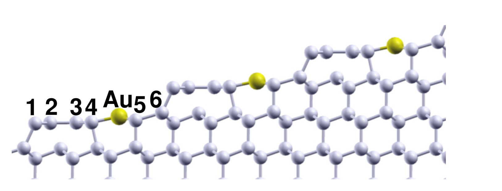
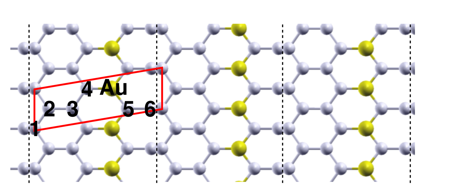
The deposition of 0.28 ML of gold on Si(335) surface forms well ordered arrays of chain structure. The surface consists of (111) terraces which have a width (1.26 nm) Zdyb . Each terrace contains a single row of gold atoms running parallel to the step edge, i.e. in the direction. The gold chain is formed by substitution of Si atoms in the middle of terrace. The step edge Si atoms form a ’honeycomb’ substructure Erwin ; Kang ; Battaglia , which is a common feature of all the Au-induced vicinal Si surfaces Crain . The structural model of the Si(335)-Au surface is shown in Fig. 1, where the Si surface atoms (Si1-Si6) are labeled by numbers 1-6, and the gold atom by Au.
Originally this model has been proposed as a simple truncation of Si(557)-Au reconstruction Crain , and later confirmed by DFT calculations MK_2 .
The STM topography data Crain ; MK_1 show a single chain per terrace, which is associated with the step edge Si atoms rather than with the Au chain. The gold substitutes some of top layer Si atoms in the middle of terrace, and is not visible to STM. This has also been confirmed by DFT calculations MK_2 . See also simulated STM topography images presented in Fig. 3. The ARPES spectra show two highly dispersive bands crossing the Fermi energy in the direction parallel to the steps, and quite flat bands in the direction perpendicular to them Crain , clearly indicating one-dimensional metallic nature of the system. The DFT calculations indicate that one of the bands crossing is associated with the step edge Si atoms, having unsaturated dangling bonds, while the other one originates from hybridization of the Au and neighboring Si atoms in the middle of terrace in the surface layer MK_2 .
IV Structural model of Pb chains on Si(335)-Au
One-dimensional structures of Pb on Si(335)-Au reconstruction one obtains assuming single Pb atom per Si(335)-Au unit cell, which corresponds to the experimental Pb coverage - 0.28 ML Kisiel_2 . The total energy calculations show that Pb atoms prefer to adsorb on the surface. The substitution of Pb atoms into top Si layer is energetically less favorable, as the surface energy is by 0.3-0.6 eV (per unit cell) higher in comparison to clean Si(335)-Au surface and Pb atom in the bulk fcc structure. Similarly, the substitution into the second Si layer is not preferred. In this case the energy cost is 1 eV. The exception is the substitution of Pb at the step edge, where the energy gain is 0.31 eV. More than 40 structural models have been investigated, and only five of them lead to stable structures. Corresponding surface energies, with respect to clean Si(335)-Au surface and bulk Pb atom, are shown in Table 1.
| model | position of Pb | surface energy (eV) |
|---|---|---|
| 1 | Si3-Au-Au | |
| 2 | Si1 (subst) | |
| 3 | Si5-Si6-Si1 | |
| 4 | Au-Si1-Si1 | |
| 5 | Si4-Au |
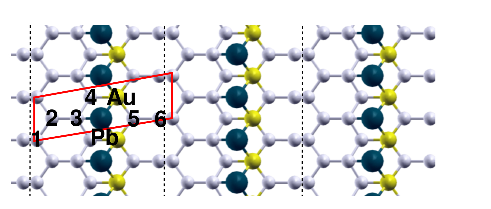
The differences in energy are rather small, however, as it will be argued later, the model with the lowest energy, i.e. Si3-Au-Au model, is the best candidate for a true model of Pb chains on Si(335)-Au surface. Note the nomenclature used here reflects the bonding of lead with corresponding surface atoms. For labeling see Fig. 2. The structural model with the lowest surface energy features Pb atoms located 2 Å above the surface near the gold chain, and is shown in Fig. 2.
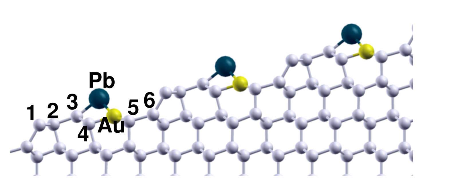
As one can read off from the figure, lead is bounded to two Au atoms and one Si3 atom, but not to Si4 atom (Fig. 2). The Pb-Si3 bond length is equal 2.75 Å, and Pb-Au - 2.92 Å. Both bonds are shorter than the Pb bonds in the bulk fcc structure (3.46 Å). The presence of Pb atoms on-top of the surface also modifies positions of underneath Au and Si atoms, leading to change in their bond lengths. Thus the Au-Si4 bond is equal 2.52 Å, and Au-Si5 - 2.47 Å, to compare with 2.43 Å and 2.38 Å, respectively, in the clean Si(335)-Au surface. What is more important, presence of Pb atoms also leads to a strong rebonding at the step edge. In the clean Si(335)-Au surface, the Si atoms near the step edge form a sort of honeycomb chain (see Fig. 1), which is common feature of all the vicinal Si surfaces Crain . Main feature of this substructure is a true double bond between Si2 and Si3 atoms, which is responsible for the stability of the honeycomb chain Erwin . In the presence of Pb atoms on Si(335)-Au surface, there is no longer double bonds between Si2 and Si3 atoms. The atoms are just single bonded, as in common silicon structures. The Si3 atom is now bonded with the lead, and Si2 with underneath Si atom in the second layer (compare Fig. 1 and Fig. 2).
At this point I would like to comment on main structural features of the other models, listed in Table 1, which have slightly higher relative surface energies. The next ’best’ structural model features the step edge Si atoms substituted by lead (model 2 in Table 1). Model 3, having relative surface energy -0.25 eV, accounts for Pb atom bonded to Si5 and Si6 atoms within the same terrace and Si1 atom at the step edge of the neighboring terrace (see Fig. 2 for labeling). In model 4, with the energy -0.06 eV, Pb is located between two Si1 atoms at the step edge and one gold atom on neighboring terrace, while in model 5 the Pb takes bridge position between Si4 and Au atoms on the same terrace. However those models can be ruled out, according to arguments given below.
The present model, i.e. the model with the lowest relative surface energy, is a good candidate for structural model of Si(335)-Au/Pb reconstruction. There are few strong arguments supporting this model. First one is that the model has the lowest energy. The second one is that the model explains the STM data of Ref. Kisiel_2 . In STM images of Si(335)-Au/Pb surface, the Pb chains are located in between the chain structure of original Si(335)-Au reconstruction (see Fig. 1 of Ref. Kisiel_2 ). According to the STM data, the Pb chains should be located in the middle of terraces, above the surface. This is exactly what the present model shows, and STM simulations, which will be presented in the next section, confirm this. The other models, listed in Table 1 remain in disagreement with the STM data. Model 1 leads to a single chain in STM topography, as the step edge Si atoms, which formed the monoatomic chains in clean Si(335)-Au surface are now replaced by the lead atoms. Similarly, models 2, 3 and 4 also lead to single chain within terrace, as the Pb atoms saturate the step edge Si dangling bonds. In fact, the STM topography of model 4 shows a zig-zag chain, associated with Pb atoms and less visible step edge Si atoms. Only the last model, i.e. model 5, remains in reasonably good agreement with STM topography data. The next argument concerns the band structure, as the only present model reproduces the photoemission spectra of Ref. Kisiel_2 very well. The other models, which have slightly higher relative surface energies disagree with the ARPES data, in particular, they do not give correct band structure near the Fermi energy. This will be further discussed in Sec. VI. The next argument, albeit intuitive, is based on the analogy with the growth of Pb on flat Si(111) surface. It is well known, that lead grows in very regular fashion, i.e. layer by layer, on Si(111)-Au(66) surface from very beginning Jalochowski_2 ; Jalochowski_3 ; Jalochowski_4 , contrary to the growth on Si(111) with 77 reconstruction, where it forms amorphous wetting layer Jalochowski_2 ; Weitering ; Budde . This indicates that Pb prefers to bond with Au rather than with Si atoms. The present model of Si(335)-Au/Pb surface also reflects this fact, as the Pb atom is bonded with one Si and two Au atoms. The last argument comes from the conditions at which the experiment of Ref. Kisiel_2 has been performed. Namely, the temperature of deposition of Pb on Si(335)-Au surface was 260 K. This temperature is far to low to substitute the Si atom by the lead, and the model with Si1 atoms replaced by Pb can be ruled out. All the above arguments show that the model shown in Fig. 2 is very good candidate to be a true model of the Pb chains on Si(335)-Au surface.
V STM simulations
The STM topography data of clean Si(335)-Au surface shows one-dimensional structures which are interpreted as the step edge Si atoms Crain ; MK_2 . The deposition of 0.28 ML of Pb leads to monoatomic Pb chains located in the middle of the Si(335)-Au terraces, i.e. between the Si chains of original Si(335)-Au surface. The structural model discussed in previous section supports this scenario. To further check the validity of the structural model, I have performed STM simulations within the Tersoff-Hamann approach Tersoff . The results of constant current topography for different bias voltages are shown in Fig. 3.
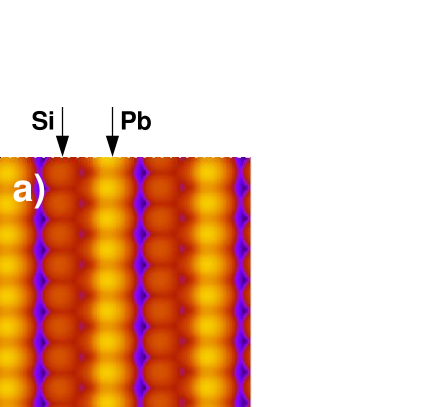
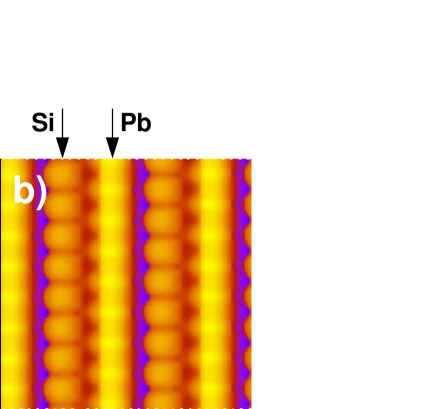
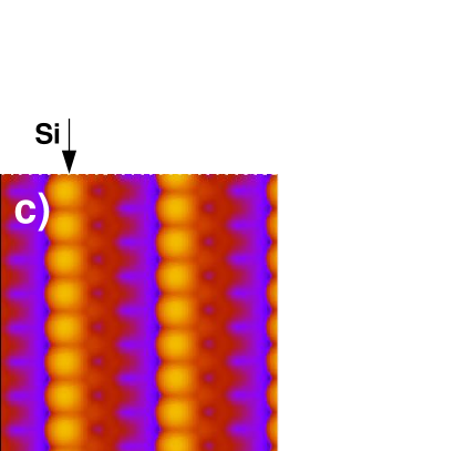
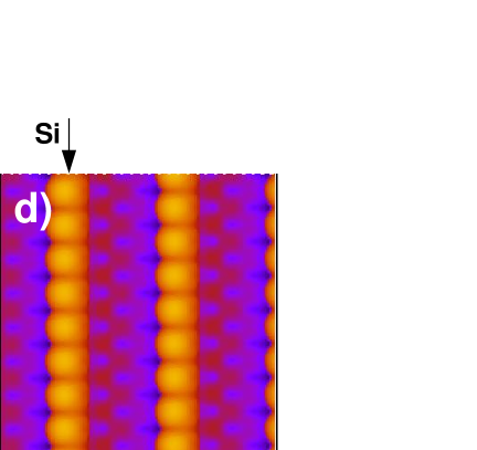
Top panels represent simulated STM topography of 3 3 nm2 of the same area of the Si(335)-Au/Pb surface for sample bias V (a) and V (b). For comparison, corresponding images of the same area of clean Si(335)-Au surface are shown in the bottom panels. As it was discussed previously (see Sec. III), the STM topography of clean Si(335)-Au surface features monoatomic chains, which are associated with the step edge Si atoms (see Fig. 3c) and d)). The Pb atoms deposited on this surface form monoatomic chains, located in the middle of terraces, i.e. between the chains of clean Si(335)-Au surface. This is evident, if one compares panels a) and c) or b) and d) of Fig. 3.
As one can read off from Fig. 3, the Pb atoms are more pronounced than the step edge Si atoms, especially at high sample bias. Such a behavior can be explained by the combination of structural end electronic effects. The Pb chain sticks out (by 2 Å ) above the surface, and this mainly contribute to the discussed effect. On the other hand, the electronic properties also play significant role. The calculated projected density of states (PDOS) of the Pb atoms and the step edge Si atoms is shown in Fig. 4.
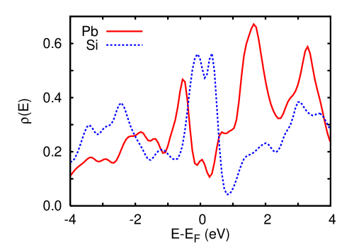
The Pb PDOS features larger values at energies eV and eV (see solid line in Fig.4), while PDOS of the step edge Si atoms is larger near the Fermi energy (dashed line). In first approximation, the STM current is proportional to integrated density of states between the Fermi energy and applied bias voltage (eU). This contributes to the fact that the Pb chain is more pronounced at higher sample bias. At very low sample bias () V, the step edge Si atoms have larger values of PDOS, and as a result both chains have comparable topography amplitude (see panel b) of Fig. 3). However, the Pb chain is still more pronounced than the Si one due to the fact that it sticks out above the surface.
The STM topography along the Pb chain shows very small changes of the amplitude at low voltages (see panel b) of Fig. 3), indicating strong overlapping of the 6p states. This is also reflected in the band structure, where 6p band of lead, crossing the Fermi energy, is very dispersive in the direction along the chain (see Fig. 4). On the other hand, there is no such an effect in the STM topography of the step edge Si atoms due to more localized character of 3p states of silicon. As a result the step edge Si band is rather flat, i.e. is less dispersive than 6p band of lead (see Fig. 4). All this shows that the Pb chain has more metallic character than the step edge Si chain, which makes the lead a good candidate to look for exotic phenomena characteristic for the systems of reduced dimensionality.
VI Band structure
The calculated band structure for present structural model, along the high symmetry lines of two-dimensional Brillouin zone (BZ), is shown in Fig. 5.
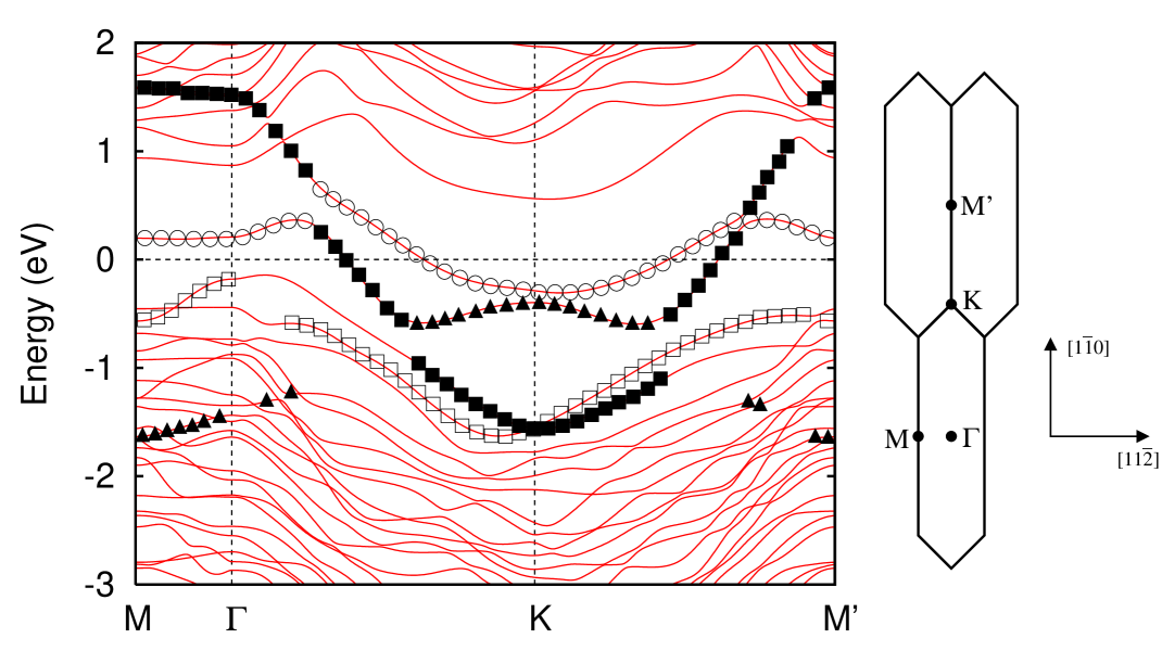
The direction in the 2D Brillouin zone, defined by the points , K and M’, is parallel to the steps of the Si(335)-Au surface, while the -M is perpendicular to them (see right panel of Fig. 5). A few important surface bands are marked with symbols in Fig. 5. The band marked with open circles pinning the Fermi energy, originates from unsaturated bonds of the Si atoms at the step edge. The band 0.5-1.5 eV below the Fermi energy (open squares), as well as more dispersive band crossing the EF (filled squares) are associated with the Au chain. To be more precise, those bands originate from the hybridization of the Au chain with neighboring Si4 and Si5 atoms (see Fig. 2). All the bands discussed above have also been identified in the clean Si(335)-Au surface MK_2 and similar bands have been found in the Si(557)-Au reconstruction Sanchez_1 ; Sanchez_2 . In fact, the band marked with filled squares has also Pb character. This band reflects the hybridization of gold with Pb and Si5 atoms. Finally, the band shown as filled triangles is associated with 6p states of lead. All the above bands do not have (or have very weak) dispersion in the direction perpendicular to the steps (-M), indicating one-dimensional character of the structure.
Since Pb features a strong spin-orbit (SO) interaction Dil ; Bihlmayer , and the low-dimensionality of the system can increase it Agrawal , it is worthwhile to comment on this effect in the Si(335)-Au/Pb system. Although the spin-orbit interaction was not included in present calculations, one can draw some conclusions appealing to the Si(557)-Au reconstruction. The measured band structure of Si(557)-Au surface shows two Au induced proximal bands crossing the EF near the K point (of ) zone with 300 meV splitting Losio ; Altmann ; Ahn ; Kisiel . An explanation of the splitting was given in terms of SO interaction Sanchez_3 . Since both Si(335)-Au and Si(557)-Au surfaces belong to the same family of vicinal surfaces (Si(335)-Au reconstruction may be considered as a simple truncation of Si(557)-Au surface), one can expect SO interaction to play similar role here. In fact, Crain et al. Crain observed small splitting of the band crossing the EF. This was interpreted as two different bands, one coming from Au-Si hybridization and the other one from the step edge Si atoms MK_2 . It is also possible that the splitting has its origin in the SO interaction, similar like in Si(557)-Au surface. On the other hand, if Pb is deposited onto Si(335)-Au surface, one would expect SO effect to be more pronounced. However, the ARPES data Kisiel_2 shows a single metallic band and thus no evidence of SO splitting. So one can conclude that if SO effect is really present in this system, certainly the splitting of the band is smaller than the energy resolution of the ARPES apparatus, which is 50 meV in this case. This is rather an intriguing result, however it can be true, as recent spin-polarized photoemission measurements report values of SO splitting as small as 15 meV in Pb deposited on Si(111) surface Dil_2 .
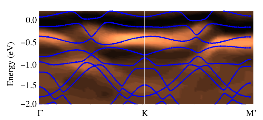
A comparison of the calculated band structure with the photoemission spectra of Ref. Kisiel_2 is shown in Fig. 6.
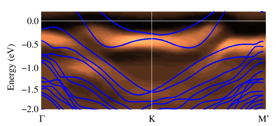
As one can see, the present DFT calculations agree very well with the experimental data. In particular, the band near the Fermi energy, which has high photoemission intensity, is the 6p band of lead. One can also identify other bands, marked with symbols in Fig. 5, except the band coming from the step edge Si atoms. The reason that this band is not observed in ARPES can be twofold. First, the band is to close to the Fermi energy which makes it very difficult to verify experimentally. Second, there may be some mechanism which leads to the saturation of the Si bonds, accounting for various imperfections or impurities. It is more likely that the band associated with the unsaturated step edge bonds (open circles in Fig. 5) is eliminated in the real surface by some reconstruction and passivation. The main effects of the reconstruction can be achieved by saturating the dangling bonds with hydrogen Sanchez_1 . This process removes extra band from the gap region (open circles in Fig. 5), and is energetically very favorable, as the energy gain is eV with respect to the unsaturated surface and H2 molecule. The comparison of the calculated band structure with saturated Si1 bonds and the ARPES spectra of Ref. Kisiel_2 is shown in Fig. 7.
Clearly, the band structure is in better agreement with the ARPES experiment now. This suggests that the step edge Si bonds are really saturated by some surface reconstruction, however this cannot be accounted for without multiplying the unit cell of the Si(335)-Au surface.
VII Step-edge buckling
The Si(557)-Au reconstruction is known to undergo a buckling of the step edge at low temperatures Sanchez_2 ; Sanchez_3 ; Riikonen . The step edge Si atoms alternate between up and down positions, with distortion in z direction Å. In general, all the step edge atoms occupy equivalent positions and feature half-filled dangling bonds, which give rise to a flat band near the Fermi energy. This is referred as high-temperature phase. However this situation is energetically unfavorable at low temperature and the system tends to lower its energy by the buckling of the step edge. The energy gain is 130.9 meV. The dangling bonds of the up-edge Si atoms became fully occupied, while those of the down-edge are empty. As a result the band structure features the fully occupied and empty step-edge electron bands. The buckling of the step edge influences the properties of the band structure near the Fermi energy through changes in the Au-Si-Au bond angles. Those changes are responsible for the band gap that opens in dispersive Au-Si band crossing the EF, and thus for the metal-insulator transition at low temperature Riikonen .
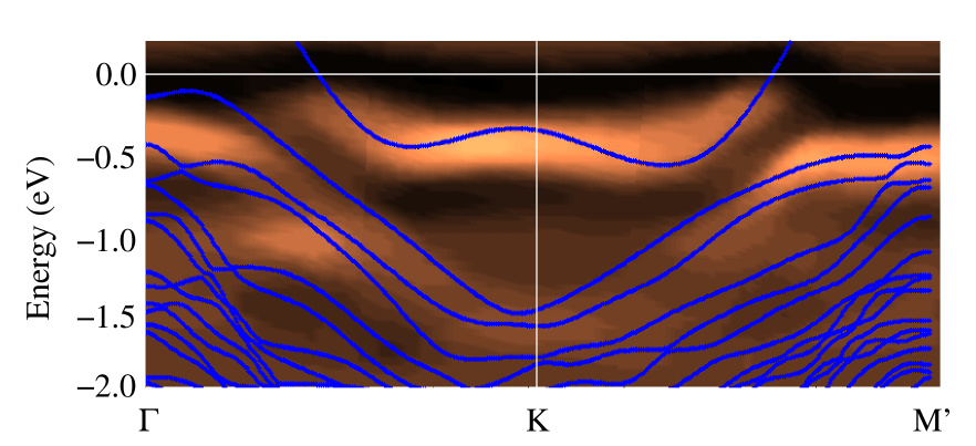
Doubling the unit cell of Si(335)-Au/Pb system in direction one can account for similar effect associated with the buckling of the step edge. In the present system the distortion is slightly smaller than in Si(557)-Au system, and equal to 0.57 Å. This smaller value of the can be related to the fact that Si(557)-Au supercell cell consists of two non-equivalent unit cells with extra Si adatom in one of them, which in turn can increase . The Si(335)-Au/Pb supercell is constructed from two equivalent cells. The buckling of the step edge lowers the total energy of the system by 117.5 meV, to be compared with 130.9 meV in the case of Si(557)-Au surface, and leads to a splitting of the step edge Si band, originally pinning the Fermi energy. As a result one observes two bands, a fully occupied flat band (with a bandwidth eV) at energy 0.29 eV below EF, and empty more dispersive band ( eV) at energy 0.25 eV above the EF. Those bands are associated with up-edge and down-edge Si atoms, respectively. Similar bands have also been observed in the Si(557)-Au surface Riikonen . The step edge buckling is also reflected in different bond angles between Au and Si5 atoms (see Fig. 2). In situation when all the step edge Si atoms occupy equivalent positions (), these angles are equal 101.64∘, to be compared with 111.6∘ and 103.7∘ for Si(557)-Au surface. Again, different values of the Si(557)-Au angles come from non-equivalent unit cells, and the buckling can change them by Riikonen . On the other hand, the buckling in the present system changes the Si5-Au-Si5 angles to 101.75∘ (up-edge) and 101.29∘ (down-edge cell). Moreover, the angles between Au and Pb atoms are also slightly changed, and equal 81.78∘ (81.54∘) in up-edge (down-edge) cells, to be compared with equilibrium value 81.97∘. All this is reflected in the band structure, where very small energy gap develops in dispersive Au-Pb-Si band (filled squares in Fig. 5), when the step-edge buckling takes place. However, this small energy gap is slightly below the Fermi level. Similar effect, although with slightly larger energy gap, has been found in Si(557)-Au surface Riikonen , and has been assigned to the shortcomings of the LDA functionals, which fail to describe excitation spectra. So one can expect that better description of the exchange and correlation effects (like GW approximation) will move the empty states to higher energies, thus driving the system into insulating state Rohlfing ; Faleev . However, it is also possible, that present LDA results are correct, and the system stays in metallic phase. The step-edge buckling may not be able to open a true gap in Au-Pb-Si band, as it gives much smaller values of Au-Si angles than in case of the Si(557)-Au surface. This last scenario seems to be supported by experimental data of Ref. Kisiel_2 , shown in Fig. 8 together with calculated surface band structure for the step-edge buckled Si(335)-Au/Pb reconstruction.
As one can see the agreement between measured and calculated band structure is very good. In particular there is no band pinned at the Fermi energy.
To calculate the surface band structure shown in Fig. 8, following procedure has been applied. Since the bulk periodicity in direction is , and calculations have been performed in unit cell in this direction, the resulting band structure features twice as many bands as in unit cell, folded back into first BZ of structure. This of course is not observed in experiment, as the ARPES is surface sensitive technique. To get rid of these bulk electron bands, only the surface atoms have been taken into account in calculations. The positions of these atoms have been obtained in full slab calculations, as described in Sec. II. To mimic rest of the Si layers, the surface Si atoms were passivated by hydrogen. The H atoms were placed in a way that the bond lengths and bond angles between surface and next from the surface Si layers were preserved. In this way calculated band structure is shown in Fig. 8. Note that differences between in this way calculated surface band structure and that obtained from full slab calculations are negligible.
VIII Conclusions
In conclusion, the structural and the electronic properties of the monoatomic Pb chains on Si(335)-Au surface have been studied within the density functional theory. The obtained structural model features Pb chain on-top of the surface in the middle of terrace. As a result, two monoatomic chains are observed on single terrace, one made of lead, and the other one associated with the step edge Si atoms. Both chains are visible in STM experimental data. The STM topography is very well reproduced within the present model. The calculated band structure shows clear one-dimensional character of the structure and remains in almost perfect agreement with the ARPES data. Finally, the buckling of the step edge Si atoms has been found, and unlike for the Si(557)-Au surface, does not drive the system into insulating phase.
Acknowledgements.
I would like to thank Prof. M. Jałochowski for valuable discussions. This work has been supported by the Polish Ministry of Education and Science under Grant No. N202 081 31/0372.References
- (1) T. Giamarchi, Quantum Physics in One Dimension (Oxford University Press, New York, 2004).
- (2) J. M. Luttinger, J. Math. Phys. 4, 1154 (1963).
- (3) O.M. Auslaender, H. Steinberg, A. Yacoby, Y. Tserkovnyak, B.I. Halperin, K.W. Baldwin, L.N. Pfeiffer, K.W. West, Science 308, 88 (2005).
- (4) R.F. Peierls, Quantum Theory of Solids (Clarendon Press, Oxford, 1955).
- (5) F.J. Himpsel, K.N. Altmann, R. Bennewitz, J.N. Crain, A. Kirakosian, J.L. Lin, J.L. McChesney, J. Phys.: Condens. Matter 13, 11097 (2001).
- (6) J.H.G. Owen, K. Miki, D.R. Bowler, J. Mater. Sci. 41, 4568 (2006).
- (7) R. Zdyb, M. Stróżak, M. Jałochowski, Vacuum 63, 107 (2001).
- (8) J.N. Crain, J.L. McChesney, F. Zheng, M.C. Gallagher, P.C. Snijders, M. Bissen, C. Gundelach, S.C. Erwin, F.J. Himpsel, Phys. Rev. B 69,125401 (2004).
- (9) M. Krawiec, T. Kwapiński, M. Jałochowski, Phys. Status Solidi B 242, 332 (2005).
- (10) M. Kisiel, K. Skrobas, R. Zdyb, M. Jałochowski, Opt. Appl. 35, 449 (2005).
- (11) M. Krawiec, Appl. Surf. Sci. 254, 4318 (2008).
- (12) P. Starowicz, O. Gallus, Th. Pillo, Y. Baer, Phys. Rev. Lett. 89, 256402 (2002).
- (13) M. Jałochowski, M. Stróżak, R. Zdyb, Appl. Surf. Sci. 211, 209 (2003).
- (14) M. Kisiel, K. Skrobas, R. Zdyb, P. Mazurek, M. Jałochowski, Phys. Lett. A 364, 152 (2007).
- (15) R. Zdyb, Appl. Surf. Sci. 254, 4408 (2008).
- (16) K. Skrobas, R. Zdyb, M. Kisiel, M. Jałochowski, Mater. Sci. - Poland 26, 55 (2008).
- (17) R. Zdyb, J. Non-Cryst. Solids 354, 4176 (2008).
- (18) M. Jałochowski, E. Bauer, Phys. Rev. B 38, 5272 (1988).
- (19) M. Jałochowski, E. Bauer, J. Appl. Phys. 63, 4501 (1988).
- (20) M. Jałochowski, M. Hoffmann, E. Bauer, Phys. Rev. B 51, 7231 (1995).
- (21) J. H. Dil, T. U. Kampen, B. Hulsen, T. Seyller, K. Horn, Phys. Rev. B 75, 161401 (2007).
- (22) P. Ordejon, E. Artacho, J.M. Soler, Phys. Rev. B 53, R10441 (1996).
- (23) D. Sanchez-Portal, P. Ordejon, E. Artacho, J.M. Soler, Int. J. Quantum Chem. 65, 453 (1997).
- (24) E. Artacho, D. Sanchez-Portal, P. Ordejon, A. Garcia, J.M. Soler, Phys. Status Solidi B 215, 809 (1999).
- (25) J.M. Soler, E. Artacho, J.D. Gale, A. Garcia, J. Junquera, P. Ordejon, D. Sanchez-Portal, J. Phys.: Condens. Matter 14, 2745 (2002).
- (26) E. Artacho, E. Anglada, O. Dieguez, J. D. Gale, A. Garcia, J. Junquera, R. M. Martin, P. Ordejon, J. M. Pruneda, D. Sanchez-Portal, J. M. Soler, J. Phys.: Condens. Matter 20, 064208 (2008).
- (27) J. P. Perdew, A. Zunnger, Phys. Rev. B 23, 5048 (1981).
- (28) N. Troullier, J. L. Martins, Phys. Rev. B 43, 1993 (1991).
- (29) S. C. Erwin, H. H. Weitering, Phys. Rev. Lett. 81, 2296 (1998).
- (30) M.-H. Kang, J.-H. Kang, Phys. Rev. B 58, R13359 (1998).
- (31) C. Battaglia, H. Cercellier, C. Monney, L. Despont, M. G. Garnier, P. Aebi, J. Phys.: Conf. Ser. 100, 052078 (2008).
- (32) H. H. Weitering, D. R. Heslinga, T. Hibma, Phys. Rev. B 45, 5991 (1992)
- (33) K. Budde, E. Abram, V. Yeh, M. C. Tringides, Phys. Rev. B 61, R10602 (2000).
- (34) J. Tersoff, D. R. Hamann, Phys. Rev. Lett. 50, 1998 (1983); Phys. Rev. B 31, 805 (1985).
- (35) D. Sanchez-Portal, J. D. Gale, A. Garcia, R. M. Martin, Phys. Rev. B 65, 081401 (2002).
- (36) D. Sanchez-Portal, R. M. Martin, Surf. Sci. 532, 655 (2003).
- (37) G. Bihlmayer, S. Blügel, E. V. Chulkov, Phys. Rev. B 75, 195414 (2007).
- (38) B. K. Agrawal, V. Singh, R. Srivastava, S. Agrawal, Phys. Rev. B 74, 245405 (2006).
- (39) R. Losio, K. N. Altmann, A. Kirakosian, J. -L. Lin, D. Y. Petrovykh, F. J. Himpsel, Phys. Rev. Lett. 86, 4632 (2001).
- (40) K. N. Altmann, J. N. Crain, A. Kirakosian, J. -L. Lin, D. Y. Petrovykh, F. J. Himpsel, R. Losio, Phys. Rev. B 64, 035406 (2001).
- (41) J. R. Ahn, W. H. Yeom, H. S. Yoon, I. -W. Lyo, Phys. Rev. Lett. 91, 196403 (2003).
- (42) D. Sanchez-Portal, S. Riikonen, R. M. Martin, Phys. Rev. Lett. 93, 146803 (2004).
- (43) H. Dil, F. Meier, J. Lobo-Checa, L. Patthey, G. Bihlmayer, J. Osterwalder, Phys. Rev. Lett. 101, 266802 (2008).
- (44) S. Riikonen, D. Sanchez-Portal, Phys. Rev. B 76, 035410 (2007).
- (45) M. Rohlfing, P. Krüger, J. Pollmann, Phys. Rev. B 52, 1905 (1995).
- (46) S. V. Faleev, M. van Schilfgaarde, T. Kotani, F. Léonard, M. P. Desjarlais, Phys. Rev. B 74, 033101 (2006).