Negative differential resistance in nanoscale transport in the Coulomb blockade regime
Abstract
Abstract
Motivated by recent experiments, we have studied transport behavior of coupled quantum dot systems in the Coulomb blockade regime using the master (rate) equation approach. We explore how electron-electron interactions in a donor-acceptor system, resembling weakly coupled quantum dots with varying charging energy, can modify the system’s response to an external bias, taking it from normal Coulomb blockade behavior to negative differential resistance (NDR) in the curent-voltage characteristics.
The switching and negative differential resistance (NDR) behavior of nanoscale systems has gained a lot of interest in the last decade, owing to the potential applications in single molecule electronics and has been observed in a variety of experimental systems, especially in the widely studied Tour molecules Tour ; Don . There have been many theoretical studies to understand this phenomenon within mainly through the one-electron picture Seminario ; Cornil ; rpati ; lakshmi_PRB ; lakshmi_jpc . There have also been a number of theoretical studies on donor-acceptor double quantum dot systems, where strong rectification has been observed Cuniberti , and others which showed NDR with variation in the dot-electrode coupling Thielmann ; Aghassi ; Paulsson or due to a detuning of the dot levels Aghassi . Another recent study has attempted to establish the conditions obeyed by the parameters involved, to find such a collapse in the current magnitudeBhaskaran_generic . Some recent experiments on double quantum dots also showed an NDR feature Ono ; tarucha and has rekindled interest in the phenomenon, occuring in the low temperature, weak-coupling limit. Theoretical studies of NDR in this single electron charging limit, is now gaining prominence and attracting a lot of research Hettler1 ; wegewis ; Hung . This regime, where mean-field descriptions usually fail, is one where electron charging energies are very high as compared to the broadenings due to average coupling, and are particularly important for small molecules which behave more like a quantum dot than a wire Datta_MB ; Bhaskaran . Since mean field methods combined with standard non-equilibrium Greens function (NEGF) negf1 ; negf3 ; negf4 ; negf5 treatment of transport is perturbative in the interaction parameter, it cannot capture the transitions between the spectrum of neutral and excited states, which can lead to a variety of interesting features in the current-voltage characteristics. The formalism that has now come to be used widely to capture molecular transport in the Coulomb blockade regime is the master or rate equation method IEEE .
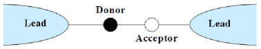
In this article, we use the above formalism to study a two-dot system consisting of a donor and an acceptor (see the schematic given in figure 1) in the Coulomb blockade regime. Taking cue from our previous mean-field transport studies on two-level systems which showed interesting non-linear behavior in their current-voltage characteristics lakshmi_PRB , here we explore the role of strong correlations in affecting their transport behavior. This study becomes interesting, especially in the context of the difference in their low-lying excitations, which would play a very important role in their low-bias current-volatage characteristics. The rate equation formalism describes transport through a correlated system with many-body eigenstates. The presence of Coulomb interactions results in occupation probabilities of each many body state that cannot be factorized as the product of the occupation probabilities of each single electron level. Hence, in this case, the full rate-equation problem, where the occupation probability of each many-body state is treated as an independent variable is solved, neglecting off-diagonal coherences. In this method, the transition rate, , from the many-body state to , differing by one electron, is calculated up to linear order in (which is the bare electron tunneling rate between the system and the electrodes), using Fermi’s golden rule as Beenakker ,
| (1) |
with a corresponding equation for and obtained by replacing by . Here, correspond to the creation/annihilation of an electron inside the dot due to electron movement from/to left (L) or right (R) electrode. and are the creation operators for electrons of spin, at the first and Nth sites respectively. We have also assumed that the creation and annihilation happen only at the terminal sites. The total transition rate is then obtained as, . The non-equilibrium probability of occurrence of each many-body state is obtained by solving the set of independent rate equations defined by through the stationarity condition at steady state. This results in a homogeneous set of equations of the size of the many-body space. Taking advantage of the normalization condition , we obtain linear equations, which can be solved using well-known linear algebraic methods. The steady state probabilities are then used to obtain the terminal current as,
| (2) |
where . Using the above prescribed method, we study a two site system described by the Hamiltonian,
| (3) |
where is the hopping strength between the sites with same spin (), are the on-site energies, is the Hubbard interaction between electrons at the same site, is the nearest-neighbor Coulomb interaction and is the external gate bias. The average charge is assumed to be unity here dotcharge . actually gives a constant shift to the energy levels with fixed number of electrons. For two sites with two electrons, the energy levels are negatively shifted by amount. Note that, there exists two quantum phases in this model with variation of interaction parameters. For the half filled ground state, with zero onsite energies, while /2 represents a spin density wave (SDW) phase, /2 corresponds to charge density (CDW) phase in thermodynamic limitHirsch ; Tsuchiizu . However, in our case with two sites, while for , the half filled ground state gives higher preference to the state with two electrons of opposite spins at one site, for , the state with one electron at each site is more prefered.
To study the transport properties through a double quantum dot system comprising of a donor and an acceptor in the weak coupling regime, we parameterize the different coupling strengths in the total system (system+leads). For perturbation theory to be valid at temperature T, we ensure that . More specifically in our calculations, we use the value of for T=300K and for T=0.66K, which are also much smaller than the corresponding charging energies, e.g. Hubbard . As our primary interest focuses on NDR effect in the system, we choose asymmetry in the onsite energy ( = - to be larger than the interdot hopping parameter (t), and vary the Hubbard around .
.
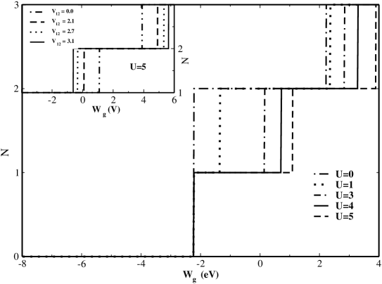
We adopt the well known exact diagonalization (ED) method to solve the Hamiltonian in equation 3 for the system containing two sites. As the total number of electrons, N, and z-component of the total spin, , commute with the Hamiltonian (H) and can be considered as conserved quantities, the H matrix can be diagonalized for a particular charge and spin sector. The Fock space then can be factored into many blocks, with largest block consisting of 4 states with quantum numbers, number of electron (N)=2 and =0. The ground state energies for N=1 (), N=2 () and N=3 () with onsite energies =0 can be easily found ()
| (4) |
Thus, the gate bias window () over which the N=2 (half-filled) state becomes lowest energy state can be estimated to be,
| (5) |
which strongly depends on the parameters involved. and are the ground state energies for 1e, 2e and 3e states respectivily in the absence of gate bias. However, with inclusion of asymmetric on-site energies, the general analytical expression for the energies become quite lengthy. For a chosen onsite energy values considering donor and acceptor sites, , we plot in figure 2 the number of electrons in the lowest energy state as a function of gate bias. This is obtained by calculating the many-body states with minimum energy at every value of gate bias as Min (). For , with increase in onsite electron-electron interaction, there is a reduction in gate bias over which two electron state is stable, while on the contrary, for , the gate bias window increases with increase in onsite electron-electron interaction. Furthermore, for values closer or greater than /2, the bias range over which two electron state is the lowest energy state, increases with increase in . This happens, because an increases in by 1eV causes no change to , an increase of 1eV to , but an increases of more than 0.5eV to for and an increase of less than 0.5eV to for . This is due to the fact that, for , two electron ground state gives higher preference to the state with two electrons of opposite spins at the site with lower on-site energy. However, for , the it prefers the state with one electron each at the donor and at the acceptor. Hence for , an increase in value by 1eV, causes an increase in the value of 2 by more than 1eV and an increase of 1eV to , so effectively reducing the value of . However for , the increase in the value of 2 is always less than 1eV and hence increases with increase in values.
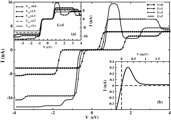
For obtaining current, for every value of and , the Fermi energy () is chosen as the value of the gate bias which ensures that two electron state is the ground state. The Fermi energy is also placed in such a way that we observe transition from the ground state to the state with one less electron. After fixing the Fermi energy, we have studied the current as a response of source-drain bias (V) in all our calculations. In figure 3, we have plotted the I-V characteristics of the system for a range of and values at room temperature. As can be seen clearly, low values of results in step-like features in I-V characterestics, while with increase in , a rise and fall in current (a NDR feature) is observed for positive values of source-drain bias. Interestingly, with inclusion of nearest-neighbor Coulomb interaction, , the I-V characteristics show wide plateau region before showing NDR feature. However, the height of the NDR peak decreases in the positive source-drain bias region with increase in . To compare our results with the experimental findings at low temperature, in the inset(b) of figure 3, we have plotted the low temperature behaviour of I-V characteristics. Note that, the NDR peak together with the overall I-V feature compare fairely well with the experimental results obtained by Tarucha et al on GaAs-based double quantum dots tarucha . We also note that, there is in fact no qualitative change in the I-V characteristics except for a constant shift in bias, if we change average dot charge() from one to zero in the Hamiltonian in equation 3.
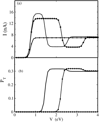
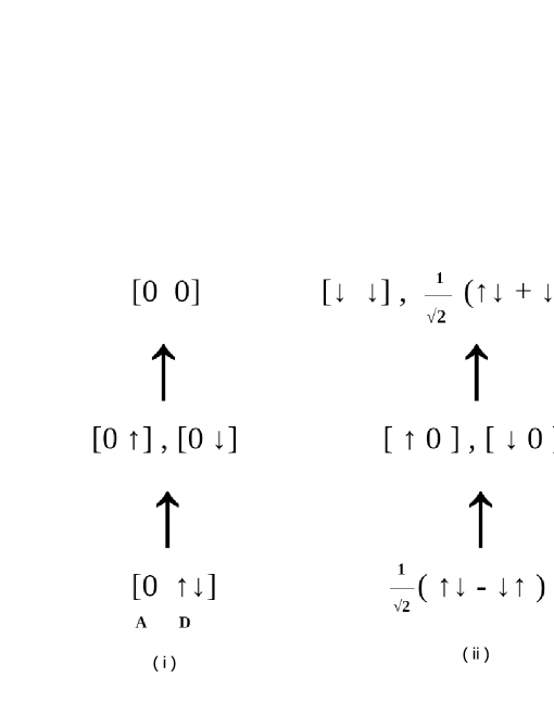
The step like feature in I-V is well understood in literature, as due to Coulomb repulsions Ratner ; Datta2 . However, to understand the NDR feature, we analyze the probabilties of occurance of various many body states. We find that NDR occurs when the source-drain bias drives the system from the 1 doublet to a higher excitation of the 2 state, namely the triplet states, instead of to the state with zero electron. It is because, when is small, the ground state gives higher preference to the state with two electrons of opposite spins at the site with lower on-site energy. This allows annihilation of an electron by the electrode followed by one more annihilation leading to a transition from the 2 singlet to the 1 doublet and then to the state with zero electron. However, when increases, the ground state gives more weightage to the state with one electron at the donor and one at the acceptor. This allows for one electron annihilation from the ground state to the 1 doublet state, followed by a creation of an electron from the same electrode to the 2 triplet state, which has the same energy as the zero electron state. Since the current at any electrode is calculated at steady state as the difference between the outgoing and incoming current, this transition results in a reduction in current leading to the negative differential resistance (NDR) peak in large limit. A schematic figure describing the states involved with increase in positive source-drain bias for small and large limits are shown in figure 4. Note that, with inclusion of , particularly for large values, the charge density modulated state gets prominance, similar to the ground state electronic configuration as in the small limit. Thus, with increase in , the NDR feature gets suppressed. Also, since with inclusion of , the gate bias range over which the 2 state remains the ground state differs, we pin the electrode’s Fermi energy in such a way that the transition from 2 singlet to 1 doublet state occurs at the same values of V (see the inset (a) of figure 3) for a range of values. However, with increase in positive bias, the electrochemical potential at the left electrode () moves down and that at right electrode () moves up, causing the transport channel is in resonance with the levels of the electrodes, where and are the energy levels associated with 2 triplet state and 1 doublet state respectively. With large values, this channel width causes the plateau in I-V characterestics to be wider before showing NDR.
To understand the NDR feature more clearly, and to estimate the height of the peak value in the I-V plot in figure 3, we calculate the probability of occurance of the 2 triplet state with increase in V for a range of Hamiltonian parameters. In figure 5, we have plotted the variation of current and the occupation probability of 2 triplet state with source-drain bias for = 5 eV. It is clear that, when the occupation probability of the 2 triplet state starts increasing appreciably, the current decreases in magnitude, however, only to a nonzero value. The main point is that the triplet state being the blocking state suppresses the current, however, since its probability of occurance does not increase more than 30%, there is still some finite current (leakage current) which flows through the system. Note that, the I-V characteristics are asymmetric because of the inherent asymmetry in the system comprising of a donor and an acceptor with different site energy () values.
In conclusion, we have studied transport behavior of donor-acceptor system in the Coulomb blockade regime through the rate equation approach. Our study shows how the variation in the on-site Coulomb repulsions can influence the system’s response to an external source-drain bias. A strong Coulombic repulsion even results in NDR for positive values of source-drain bias in the I-V characteristics. Also, a strong nearest-neighbour Coulomb interaction suppresses the NDR like feature, taking back the system to normal Coulomb staircase regime.
Acknowledgement: PP acknowledges the CSIR for a research fellowship and SKP acknowledges research support from CSIR and DST, Government of India and AOARD, Asian Office.
References
-
(1)
Chen J, Reed M A, Rawlett A M and Tour J M 2001 Science 286 1550
Chen J, Wang W, Reed M A, Rawlett A M, Price D W and Tour J M 2000 Appl. Phys. Lett. 77 1224 - (2) Donhauser Z J, Mantooth B A, Kelly K F, Bumm L A, Monnell J D, Stapleton J J, Price D W, Jr, Rawlett A M, Allara D L, Tour J M and Weiss P S 2001 Science 292 2303
-
(3)
Seminario Jorge M, Zacarias Angelica G and Tour J M 2000 J. Am. Chem. Soc. 122 3015
Seminario J M, Zacarias Angelica G and Derosaet Pedro A 2002 J. Chem. Phys. 116 1671 -
(4)
Cornil J, Karzazi Y and Brédas J L 2002 J. Am. Chem. Soc. 124 3516
Lakshmi S and Pati S K 2004 J. Chem. Phys. 121 11998 - (5) Pati R and Karna S P 2004 Phys. Rev. B. 69 155419
- (6) Lakshmi S and Pati S K 2005 Phys. Rev. B. 72 193410
- (7) Lakshmi S, Dutta S and Pati S K 2008 J. Phys. Chem. C 112 14718
- (8) Thielmann A, Hettler M H, Konig J and Schon G 2005 Phys. Rev. B. 71 045341
- (9) Hettler M H, Wenzel W, Wegewijs M R and Schoeller H 2003 Phys. Rev. Lett. 90 076805
- (10) Wegewis M R, Hettler M, Wenzel Wolfgang and Schoeller Herbert Physica E 18 241
- (11) Hung Nguyen V, Lien Nguyen V and Dollfus P 2005 Appl. Phys. Lett. 87 123107
- (12) Song B, Ryndyk D A and Cuniberti G 2006 Preprint cond-mat/0611190
- (13) Aghassi Jasmin, Thielmann Axel, Hettler Matthias H and Schön Gerd 2006 Phys. Rev. B. 73 195323
- (14) Paulsson M and Stafstrom S 2001 Phys. Rev. B 64 035416
- (15) Muralidharan B and Datta S 2007 Preprint cond-mat/0702161
- (16) Ono K, Austing D G, Tokura Y and Tarucha S 2002 Science 297 1313
- (17) Ono K and Tarucha S 2004 Phys. Rev. Lett. 92 256803
- (18) Muralidharan B, Ghosh A W and Datta S 2006 Phys. Rev. B 73 155410
- (19) Datta S 2004 Nanotechnology 15 S433
- (20) Caroli C, Combescot R, Lederer D, Nozieres P and Saint-James D 1971 J. Phys. C 4 2598
- (21) Palacios J J, Pérez-Jiménez A J, Louis E and Vergés J A 2001 Phys. Rev. B 64 115411
- (22) Rocha R and Sanvito S 2004 Phys. Rev. B 70 094406
- (23) Ferrer J, Martín-Rodero A and Flores F 1988 Phys. Rev. B 38 R10113
- (24) Muralidharan B, Ghosh A W, Pati S K and Datta S 2007 IEEE Transac. on Nanotech. 6 536
-
(25)
Beenakker C W J 1991 Phys. Rev. B 44 1646
Hettler M H, Schoeller H and Wenzel W 2002 Europhys. Lett. 57 571 - (26) Pati S K, Ramasesha S, Shuai Z and Bredas J L 1999 Phys. Rev. B 59 14827
- (27) Hirsch J E 1984 Phys. Rev. Lett. 53 2327
- (28) Tsuchiizu M and Furusaki A 2002 Phys. Rev. Lett. 88 056402
- (29) Mujica Vladimiro, Kemp Mathieu, Adrian Adrian and Ratner Mark 1996 J. Chem. Phys. 104 7296
- (30) Muralidharan B and Datta S 2007 Phys. Rev. B 76 035432