Observation of chiral quantum-Hall edge states in graphene
Abstract
In this study, we determined the chiral direction of the quantum-Hall (QH) edge states in graphene by adopting simple two-terminal conductance measurements while grounding different edge positions of the sample. The edge state with a smaller filling factor is found to more strongly interact with the electric contacts. This simple method can be conveniently used to investigate the chirality of the QH edge state with zero filling factor in graphene, which is important to understand the symmetry breaking sequence in high magnetic fields (25 T).
pacs:
73.43.Fj, 72.80.Rj, 73.23.-b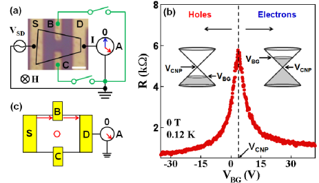
At a quantum-Hall (QH) plateau in a two-dimensional (2D) electron system, conducting electrons in the QH edge states circulate in one direction (a chiral direction) without any dissipation. Klitzing80 ; Halperin82 ; Buttiker88 These QH edge states can be conveniently used to build quantum devices such as a solid-state electronic beam splitter. Ji03 In graphene, a honeycomb lattice of -bonded carbon atoms, the relativistic character of the Dirac-fermionic carriers exhibits the half-integer QH effect, Neto09 which is distinctive from the integer QH effect in ordinary 2D electronic systems. Klitzing80 It has been generally believed that carriers in the QH edge states in graphene also circulate in one direction (one chirality), either clockwise or counterclockwise, as in a conventional 2D electron gas for a fixed perpendicular magnetic field. Abanin07-2 ; Williams07 ; Ozyilmaz07 The chiral properties of the QH edge states are important, in particular, in a strong-enough magnetic field as to break either the spin or pseudospin symmetry, which leads to the QH plateau of zero filling factor. Zhang06 ; Abanin07 ; Jiang07 ; Checkelsky08 ; Checkelsky09 Depending on whether the spin or the pseudospin symmetry is broken first, graphene becomes either ferromagnetic or insulating, respectively. Abanin07-1 ; Gusynin08 In the QH ferromagnetic state, Zhang06 ; Abanin07 ; Jiang07 the QH edge carriers in the zero plateau are believed to be in a counter-circulating state, but in the QH insulating state, Checkelsky08 ; Checkelsky09 the edge states themselves do not exist.
In this study, we examined the chiral direction of the QH edge states in graphene by using a simple two-terminal transport measurement scheme while grounding different edge positions of the sample. Reduction and recovery of the conductance were observed depending on the position of the grounded edge contacts (ECs), on the back-gate (BG) voltage (), and on the magnetic-field direction. Our study indicates that the QH edge states in graphene also possess the chirality, Halperin82 ; Buttiker88 ; Ki09 and, moreover, the edge states corresponding to smaller filling factors are more strongly coupled with the electrical contacts. Krstic08
Monolayer graphene sheets were mechanically exfoliated Novoselov04 onto a highly doped silicon substrate covered with a 300-nm-thick oxidation layer, where the substrate served as the global BG. The device [Fig. 1(a)] was fabricated by the sequential e-beam lithography and the electrode metallization by evaporation. Ki08 The sample was cooled down to 120 mK in a dilution fridge (Oxford Instruments, Model Kelvinox), where electric noises were filtered out by connecting low-pass RC and filters in series. Ki08 At the base temperature, the two-terminal conductance (=/) was measured using the conventional lock-in technique operated at 13.33 Hz while monitoring the current with a current preamplifier for the source-drain bias voltage () of 30 V. The measurement configuration is illustrated in Fig. 1(a).
Figure 1(b) shows the electric-field control of the conducting charge carriers, Neto09 which reveals a resistance maximum at 3.8 V. At this charge neutrality point (), the carriers changes from being holelike to being electronlike with increasing [see the inset of Fig. 1(b)]. Neto09 As shown in Fig. 1(b), the resistance asymmetry is present between the hole and the electron sides, i.e., the mobility () of the device differs as the carrier type varies. The value of is 3600 cm2V-1s-1 (4500 cm2V-1s-1) for =30 V (-20 V). This electron-hole asymmetry may arise from the unintended chemical doping of the graphene sheet in the fabrication process Farmer09 or the charge pinning at the interface of invasive metallic contacts and the graphene sheet. Huard08
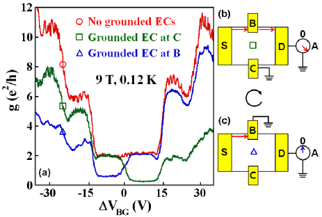
Figure 2(a) displays the two-terminal conductance in units of =e2/h as a function of with respect to (=) measured in =9 T [see Fig. 1(a) for the positive field direction]. The total contact resistance including the resistance of low-pass RC filters connected in series, 4.3 k, was obtained independently and subtracted from the measured two-terminal conductances. With the EC electrodes B and C being floated, a clear conductance plateau at 2 is observed in the region of -15 V15 V (open circle). Moreover, the clear plateaus at 6 and 10 in the hole side (0) indicate the occurrence of the half-integer QH effect, which confirms the single-layeredness of our graphene sheet. Williams07 ; Ozyilmaz07 ; Abanin08 ; Williams08 The distorted 6 and 10 plateaus in the electron side (0) are believed to arise from the reduced zero-field mobility of our graphene sheet in the electron side [Fig. 1(b)]. Similar distortion of the two-terminal conductance has been suggested Abanin08 and experimentally confirmed as well. Williams08
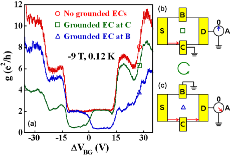
As denoted by the open square symbol in Fig. 2(a), the conductance plateau at 2, with the EC grounded at the electrode C, remains unaltered for 0 (the hole side) while it vanishes almost completely for 0 (the electron side). On the contrary, the open-triangle data, which were obtained with the EC grounded at B, show a significant reduction of the conductance in the hole side while the conductance in the electron side recovers the value without grounded ECs. The reduction of the conductance occurs as the conducting carriers are leaked to ground before they reach the drain (D) where the current detector A is located [Fig. 1(a)]. Thus, the result in Fig. 2(a) clearly indicates that the hole-like and the electron-like carriers in the edge states of QH plateaus circulate in the opposite directions with each other. To further confirm our reasoning, we measured in a negative magnetic field (-9 T) as shown in Fig. 3(a), with the contact resistance being subtracted. With no grounded ECs, the open-circle data show almost the same feature as the corresponding open-circle data in Fig. 2(a), along with distorted QH plateaus in the electron side. However, the open square (triangle) data nearly coincide with the open triangle (square) data in Fig. 2(a). This indicates that the reduction and recovery of depend on the position of the grounded EC, the carrier type, and the magnetic field direction.
The observed reduction and recovery of the conductance can be explained by assuming that the chiral property of the QH edge states in graphene is the same as the one in an ordinary 2D electron gas. Halperin82 ; Buttiker88 As illustrated in Fig. 1(c), holes (electrons) in graphene in QH plateaus flow along the upper side of the sample between the source (S) and the drain (D) in a positive (negative) magnetic field, which corresponds to the clockwise QH edge state. For simplicity, schematics of the QH edge state circulation are illustrated in the figures only for the hole side at a positive . Consequently, with no grounded ECs, charge carriers are not impeded until they reach the drain D, so that becomes the Hall conductance as shown by the open-circle symbols in Figs. 2(a) and 3(a). Buttiker88 ; Williams07 ; Ozyilmaz07 ; Abanin08 ; Williams08 On the other hand, if a grounded EC is placed in the way of the QH edge state circulation between S and D, electric charges are diverted to ground before they reach D. The consequent vanishing of current leads to the reduction of the conductance, as illustrated in Figs. 2(c) and 3(b) for the clockwise and counterclockwise QH edge states, respectively. By contrast, if an EC is grounded in the opposite side of the sample in the circulation path, the current is not drained to ground before reaching the drain D, resulting in the recovery of the conductance as illustrated in Figs. 2(b) and 3(c).
Up to this point, we assume that conducting carriers are always emitted from the source S, i.e., a positive (negative) for hole (electron) carriers. But, if hole (electron) carriers are emitted from both D and the grounded EC for a negative (positive) , the conductance reduction occurs as the same amount of holes (electrons) enter into and leave from D simultaneously with vanishing current . Thus, the results in Figs. 2(a) and 3(a) directly confirm that the QH edge states in graphene also behave in the same way as those in an ordinary 2D electron gas, whose chiral direction depends on the carrier type and the magnetic field direction. Halperin82 ; Buttiker88
The imperfect reduction and recovery of are seen in Figs. 2(a) and 3(a) for 15 V and -15 V, which suggest that the coupling strength between the electric contacts and the QH edge states is not uniform for different filling factors. Krstic08 It is because the QH edge states with smaller filling factors circulate closer to the edge of a sample, Halperin82 ; Buttiker88 with stronger coupling with the electric contacts near the edge. Therefore, a fraction of carriers in the QH edge states with higher filling factors of 6 and 10 either reach the drain D by passing the grounded EC in the way of the carrier circulation (corresponding to the imperfect reduction) or are drained at the grounded EC in the path after passing the drain D (corresponding to the imperfect recovery). The coupling is expected to be stronger for a larger contact area of the ECs, which explains why the conductance 2 shows the full recovery but with the imperfect reduction.
In summary, we made simple two-terminal conductance measurements to clarify the chiral properties of the QH edge states in graphene, which is important to design delicate functionalities in graphene-based quantum devices. Experimental findings directly support that the QH edge states in graphene are chiral in the same way as those in an ordinary 2D electron gas in low magnetic fields Halperin82 ; Buttiker88 ; Ki09 (9 T). In addition, from the imperfect reduction and recovery observed in the experiment, we demonstrate that the coupling strength between the QH edge states and the electric contacts varies depending on the filling factors as well as the contact area. Krstic08 This simple two-terminal conductance-measurement scheme can be conveniently adopted to study the chiral direction of the QH edge state of zero filling factor in graphene in a stronger magnetic field Zhang06 ; Abanin07 ; Jiang07 ; Checkelsky08 ; Checkelsky09 (25 T), to clarify the quantum state between the two contradicting models leading to the QH ferromagnets and the QH insulators. Abanin07-1 ; Gusynin08
This work was supported by Acceleration Research Grant (R17-2008-007-01001-0) by Korea Science and Engineering Foundation.
References
- (1) K. v. Klitzing, G. Dorda, and M. Pepper, Phys. Rev. Lett. 45, 494 (1980).
- (2) B. I. Halperin, Phys. Rev. B 25, 2185 (1982).
- (3) M. Büttiker, Phys. Rev. B 38, 9375 (1988).
- (4) Y. Ji, Y. Chung, D. Sprinzak, M. Heiblum, D. Mahalu, and H. Shtrikman, Nature (London) 422, 415 (2003).
- (5) For the recent review, see A. H. Castro Neto, F. Guinea, N. M. R. Peres, K. S. Novoselov, and A. K. Geim, Rev. Mod. Phys. 81, 109 (2009).
- (6) D. A. Abanin and L. S. Levitov, Science 317, 641 (2007).
- (7) J. R. Williams, L. DiCarlo, and C. M. Marcus, Science 317, 638 (2007).
- (8) B. Özyilmaz, P. Jarillo-Herrero, D. Efetov, D. A. Abanin, L. S. Levitov, and P. Kim, Phys. Rev. Lett. 99, 166804 (2007).
- (9) Y. Zhang, Z. Jiang, J. P. Small, M. S. Purewal, Y. W. Tan, M. Fazlollahi, J. D. Chudow, J. A. Jaszczak, H. L. Stormer, and P. Kim, Phys. Rev. Lett. 96, 136806 (2006).
- (10) D. A. Abanin, K. S. Novoselov, U. Zeitler, P. A. Lee, A. K. Geim, and L. S. Levitov, Phys. Rev. Lett. 98, 196806 (2007).
- (11) Z. Jiang, Y. Zhang, H. L. Stormer, and P. Kim, Phys. Rev. Lett. 99, 106802 (2007).
- (12) J. G. Checkelsky, L. Li, and N. P. Ong, Phys. Rev. Lett. 100, 206801 (2008).
- (13) J. G. Checkelsky, L. Li, and N. P. Ong, Phys. Rev. B 79, 115434 (2009).
- (14) D. A. Abanin, P. A. Lee, L. S. Levitov, Solid State Commun. 143, 77 (2007).
- (15) For a review, see V. P. Gusynin, V. A. Miransky, S. G. Sharapov, and I. A. Shovkovy, Low Temp. Phys. 34, 778 (2008).
- (16) In the recent study on the bipolar p-n-p junction of graphene, the chiral-direction-dependent asymmetric Hall resistance was observed. D. K. Ki and H. J. Lee, e-print arXiv:0903.0213.
- (17) V. Krstic, D. Obergfell, S. Hansel, Geert L. J. A. Rikken, J. H. Blokland, M. S. Ferreira, and S. Roth, Nano. Lett. 8, 1700-1703 (2008).
- (18) K. S. Novoselov, A. K. Geim, S. V. Morozov, D. Jiang, Y. Zhang, S. V. Dubonos, I. V. Grigorieva, and A. A. Firsov, Science 306, 666-669 (2004).
- (19) D. K. Ki, D. Jeong, J. H. Choi, H. J. Lee, and K. S. Park, Phys. Rev. B 78, 125409 (2008).
- (20) D. B. Farmer, R. Golizadeh-Mojarad, V. Perebeinos, Y. M. Lin, G. S. Tulevski, J. C. Tsang, and P. Avouris, Nano Lett. 9, 388 (2009).
- (21) B. Huard, N. Stander, J. A. Sulpizio, and D. Goldhaber-Gordon, Phys. Rev. B 78, 121402(R) (2008).
- (22) D. A. Abanin and L. S. Levitov, Phys. Rev. B 78, 035416 (2008).
- (23) J. R. Williams, D. A. Abanin, L. DiCarlo, L. S. Levitov, and C. M. Marcus, e-print arXiv:0810.3397.