Influence of structural disorder and large-scale geometric fluctuations on the Coherent Transport of Metallic Junctions and Molecular Wires
Abstract
Structural disorder is present in almost all experimental measurements of electronic transport through single molecules or molecular wires. To assess its influence on the conductance is computationally demanding, because a large number of conformations must be considered. Here we analyze an approximate recursive layer Green function approach for the ballistic transport through quasi one-dimensional nano-junctions. We find a rapid convergence of the method with its control parameter, the layer thickness, and good agreement with existing experimental and theoretical data. Because the computational effort rises only linearly with system size, this method permits treatment of very large systems. We investigate the conductance of gold- and silver wires of different sizes and conformations. For weak electrode disorder and imperfect coupling between electrode and wire we find conductance variations of approximately 20%. Overall we find the conductance of silver junctions well described by the immediate vicinity of narrowest point in the junction, a result that may explain the observation of well-conserved conductance plateaus in recent experiments on silver junctions. In an application to flexible oligophene wires, we find that strongly distorted conformations that are sterically forbidden at zero temperature, contribute significantly to the observed average zero-bias conductance of the molecular wire.
I Introduction
The study of electron transport properties at the molecular or even atomic scale has generated many striking insights in the last decade Nitzan and Ratner (2003); Kwiatkowski et al. (2008); Heurich et al. (2002); Oetzel et al. (2008). Many features of the measured transport characteristics of molecular wires in breakjunctions or AFM/STM setups Reed et al. (1997); Cui et al. (2001) could be explained on the basis of the Landauer formalism. There has been tremendous progress in the characterization of metallic nano-wires Scheer et al. (1997, 1998); Agrait et al. (2003); Thygesen and Jacobsen (2003); Xie et al. (2004), organic nano-wires Tao (2006); Choi et al. (2008) and nanotubes Tans et al. (1997); Postma et al. (2001); McEuen and Park (2004). Unfortunately, due to the complexity of the experimental setup, most of these measurements have no control over the details of the electrode geometry, which results in a spectrum of IV-characteristics. In the face of these and other uncertainties theoretical models can help understand and explain the experimental data Rodrigues et al. (2002)). These calculations are challenging because the electronic structure of the central cluster of the junction (,,extended molecule”), comprising the molecular wire and some part of the electrode fragments, must be computed in atomistic models. Because of the high cost of accurate electronic structure calculations, IV-characteristics are often computed for idealized geometries and electrode configurations Strange et al. (2008).
Due to computational limitations most theoretical studies of molecular junctions have employed idealized junction geometries, including placement and contact of the molecule with respect to the electrode, as well as the electrode geometry. Many present day fabrication techniques for nanojunctions entail strong deformations of the system, e.g. rupture of electrode wires (in break-junctions) and subsequent contacting procedures, which make it unlikely that ideal junction geometries are ever realized in practice. Despite the use of accurate electronic structure methods, only semi-quantitative agreement with the measured conductance has been obtained in a number of studies to date. Imperfect electrode geometries and contacts are likely to contribute to this widely discussed discrepancy Evers et al. (2004), but are difficult to assess experimentally.
The effects of structural disorder, of impurities and non-ideal electrode geometries are difficult to asses with transport methods that relies on computationally demanding ab-initio electronic structure theory, which often scale as with the system size. One possibility to take such effects into account is to develop efficient approximationsAndrews et al. (2008), which allow for inclusion of larger electrode fragments in electronic structure calculation of the ,,extended molecule” region. While such approximate methods may not predict the absolute value of the conductance quantitatively, they may help explain differential features that may originate from the existence of a large structural ensemble in the junction geometry. Such methods are also useful to investigate the coherent transport properties in very large, complex molecules, for which high-accuracy calculations remain infeasible to date.
In previous work tight binding models were successfully applied by Pauly et al. Pauly et al. (2006) to investigate conductance histograms and strain forces of Ag, Pt and ferromagnetic Ni break junctions. Additionally Häfner et al. Häfner et al. (2008) studied the influence of the absence of magnetic domains in the ferromagnetic 3 materials Fe, Co and Ni. In the case of metal-molecule-metal junctions based on oligophenylene wires the length-dependent conductance and thermopower as well as elastic and photo-assisted transport properties, a -orbital tight binding model has given intriguing insights Pauly et al. (2008a); Viljas et al. (2008).
In this paper we investigate convergence of a recursive layer Green’s function (RLGF) approachVergés (1999) that scales linearly with the system size. This approach permits the treatment of very large systems comprising more than a thousand atoms, e.g. DNA van Zalinge et al. (2006) or the atomic transistor Xie et al. (2008a), as well as computations of ensembles of thousands of structural models for disordered systems. We first analyze the truncation effects on the accuracy of conductance calculations for a several systems, where much experimental and theoretical data is available. Gold Novaes et al. (2006); Rego et al. (2003) and silver Pauly et al. (2006); Rodrigues et al. (2002) molecular wires are among the most widely studied systems in molecular electronics. We find that even for metallic systems, where the electronic wave functions are most extended, the conductance converges rapidly with the truncation cutoff parameter and converges to values in good agreement with experiment and accurate prior studies Pauly et al. (2008a); Strange et al. (2008), at a fraction of their computational cost.
Next we apply this method to novel, computationally challenging applications on transport through molecular wires. We investigated different scenarios for static and dynamic disorder in metalScheer et al. (1997, 1998); Agrait et al. (2003); Thygesen and Jacobsen (2003); Xie et al. (2004); Novaes et al. (2006); Rego et al. (2003); Pauly et al. (2006); Rodrigues et al. (2002) and metal-organic molecularChoi et al. (2008) wires. In an application on the influence of a non-vanishing tilt- and twinning-angle between the source/drain electrode tips and find a variation of up to 20% in the zero bias conductance. Additionally we probe the effect of randomly introduced surface vacancies on the electrode tips, which can lower the conductance by up to 30%.
We then turn to silver nano-clusters, which are promising systems for applications as electronic materials and for surface nano-structuring. While their structural properties have been extensively investigated Jonathan and Wales (1998); Shao et al. (2008); Ledo et al. (2007); Ramnani et al. (2007), much less is known about their transport properties. We present the first theoretical study of electronic transport through large clusters (260 atoms) and study the dependence of the transport properties on the structure and size of the nano-cluster.
While these examples concern mononuclear systems, the presence of metal-organic junctions significantly complicates the physics of nanoscale transport. Charge transfer, differences in the accuracy of the description of electronic structure of the electrode and the organic molecule, as well as other factors, complicate the theoretical description of such systems Heimel et al. (2006); Preuss et al. (2005). We have investigated the effect of dynamic disorder on the zero-bias conductance of oligophenylene molecular wires as a function of their length and geometry. We compare the total transmission function obtained by the layer approximation with the full device calculation and find a good quantitative agreement at a fraction of the computational cost.
Recent investigations have focused on the importance of even small scale geometric fluctuations on molecular transport. Here we extend this work to the first investigation of large-scale conformational change. We generate a large thermodynamically relevant ensemble of, which include complete ring-flips of the molecules, comprising thousands of conformations, to discuss the dependence of the conductance change on the torsion angle fluctuations. We find this system to be a striking example, where large scale structural fluctuations significantly affect the conductance. Configurations, which are sterically forbidden at low temperature, contribute significantly to the overall time-average of the zero-bias conductance.
II Methods
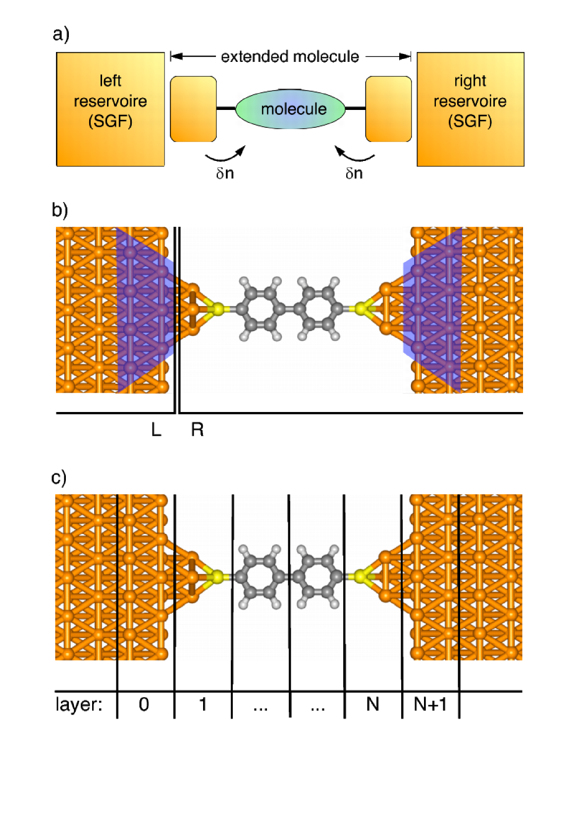
The electronic conductance of nanoscale junctions is often analyzed in the framework of Landauer theory Landauer (1970); Büttiker et al. (1985), which divides the system conceptually into idealized electrodes and a central region called ,,extended molecule”, that contains the nanojunction of interest (see Figure 1a). Using Landauer’s formula, the current is computed as:
| (1) |
where denotes the total transmission function. In order to evaluate the transmission function of the extended molecule, we must compute its electronic structure in an adequate atomistic model Damle et al. (2002). Equation (1) stipulates the existence of perfect Fermi-seas at the appropriate chemical potential of the electrodes. For these quantities to have meaning, electrode fragments must be included into of sufficient size into the extended molecule region, so that charge transfer and image-charge effects can be taken into account Heimel et al. (2006); Preuss et al. (2005). The extended molecule for which the transmission must be computed may thus be much larger than the physical object which is placed between the electrodes. In particular for homonuclear systems, such as metallic wires, there is no clear-cut distinction between electrode and ”system” at all.
To compute the current, we consider the total charge of the system on the right side of an arbitrary division of the system into a right (R) and left (L) part, respectively (see Figure 1(b)):
| (2) |
where creates an electron in orbital and the sum runs over all orbitals on the right hand side. The current can then be obtained in perturbation theory from the equation of motion , where
| (3) |
defines the velocity operator Vergés (1999). In the expression of the electron velocity operator the indices and run over the orbitals in the left (L) and right (R) parts of the system, respectively. is proportional to the transfer matrix element times the electron propagation, expressed by the particle creation and annihilation operators and , respectively. Calculation of the charge flux at any arbitrarily chosen interface is thus sufficient to obtain the total current through the system.
Using Kubo’s formula Vergés (1999); Damle et al. (2002) we can evaluate the coherent zero bias transmission at as
| (4) |
The imaginary part of the Green’s function is related to the advanced/retarded Green’s functions by
| (5) |
The computation of in general requires the inversion of the Hamilton operator of the extended molecule of the system. The computational effort of this calculation grows rapidly with the system size (i.e. the total number of orbitals), restricting the size of the system and the complexity of the electrode fragments that can be included in the extended molecule.
For this reason, we divide the extended molecule into a set of principal layers perpendicular to the current flow direction and describe the electrons contained in one principle layer with a block Hamiltonian matrix. This introduces a truncation parameter which was found to be well converging with an increasing layer thickness (see results section A). We take only these overlap matrix elements into account, which belong to nearest neighboring layers and obtain a Hamiltonian matrix of band-diagonal type. The main advantage of this approach is that the computational effort of the matrix inversion scales linearly with the system size.
We employ this feature in the evaluation of the transmission function using a Recursive Green’s function schemeVergés (1999). This method is based on an iteration over the principal layers from the left end to the right end of the extended molecule. For every layer we calculate the Green’s function by inverting the corresponding block Hamiltonian and take the influence of the semi infinite right region via self energies into account. The iteration ends up with the calculation of the Green’s function of the left most principal layer, which is plugged together with the surface Green’s function and the corresponding coupling matrixes into Kubos formula for conductance.
The whole method is based on the assumption of non-interacting electrons permitting the use of a tight binding like model Hamiltonian (extended Hückel), that allows for an efficient computation of the electronic structure during a dynamic process. More details of the numerical methods are described in the appendix.
III Results
III.1 Convergence of the layer approximation
Metallic nanowires have been among the first and most widely studied systems in molecular electronics Pauly et al. (2006); Novaes et al. (2006); Rego et al. (2003); Rodrigues et al. (2002). Metallic systems are often most challenging for linear-scaling electronic structure methods, because the electronic wave functions are extended. To provide a stringent test for our ,,local” approximation, we have investigated the convergence of the layer approximation for two representative examples, namely gold- and silver-wires respectively.
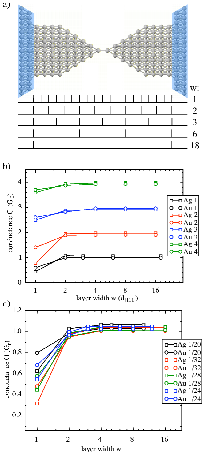
We begin the investigation by dividing silver and gold model junctions into a set of ,,principal layers” with increasing thickness . In order to establish the convergence of the method for large systems, the test geometry has to be of sufficient length. Here we investigate junctions of 45.2 Å length in -direction, containing 388 silver or gold atoms with a nearest neighbor distance of 2.88 Å in both metals Guang-Can (2006); Qian et al. (2006). We prepare the electrodes as perfect fcc-clusters, which narrow towards the center to form a single-atom point contact at their tips, generating a dimer structure which permits a current flow in the crystallographic [111] direction. The extended molecule region and the layer divisions are illustrated in Fig. 2a. The bulk electrodes are designated by the two larger layers on each side of the system.
We calculate the conductance for varying widths d[111] of the ,,principal layers” (Fig. 2a), i.e. the full length of the extended molecule region. Figure 2b shows that the conductance of the silver and gold model junction as a function of the principal layer thickness converges rapidly to the experimental value. The same holds true for the junction conformations labeled Ag 1 - Ag 4 and Au 1 - Au 4, which have a minimum cross section of 1-4 atoms, respectively. Furthermore, we calculated the convergence of the conductance for longer wire geometries (Fig. 2c), constructed by sequentially introducing additional atoms into the point contact at the minimum cross section. Thereby we obtain silver and gold junctions of 20, 24, 28 and 32 atomic layers in the -direction.
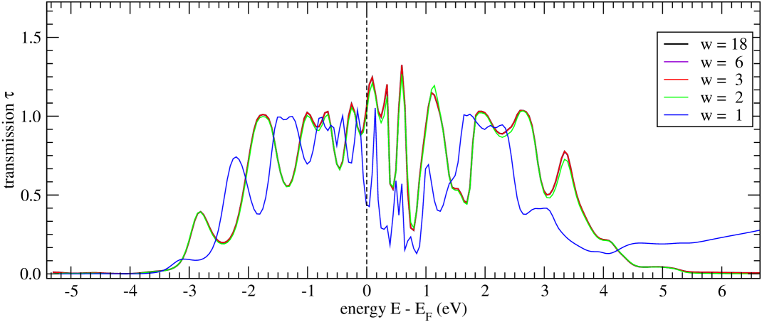
For the conductance is significantly underestimated to approximately 0.5 G0 for both metals, indicating that hopping processes across distances larger than the interatomic distance are important. For all choices of the layer thickness with the conductance has converged to nearly the experimental values. For the layer division retains the symmetry of the [111] crystal stacking order ”ABCABC…” in fcc-latices. We investigate the convergence in more detail at the level of the transmission in Fig 3, which shows the total transmission function of the geometry shown in Fig. 2a over an energy interval . Again we find that all curves for agree well with one-another.
In order to demonstrate the efficiency of this method we compare the computation time of the transmission curves shown in Fig 2. With a resolution of meV the transmission of the system divided into 1, …, 18 layers required 1368, 594, 429, 336, and 294 seconds, respectively. Using this approximation, e. g. with 6 principal layers, that takes 31% of the time of the ,,full-device” calculation, while increasing only a neglectable los of accuracy.
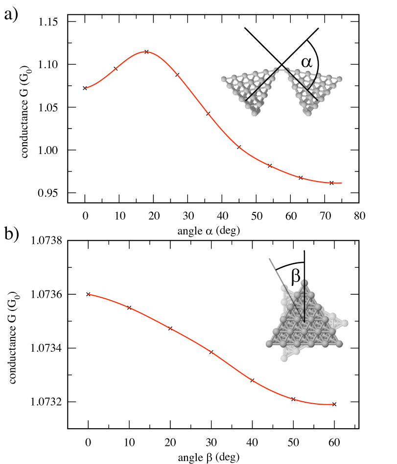
III.2 Imperfect Electrode Geometries
There are two obvious parameters which define the junction geometry with respect to the electrodes that are presently not under experimental control: the tilt and twinning angles of the two electrode fragments with respect to one another. In order to investigate the dependence of the conductance on these parameters, we have prepared a ideal fcc-silver junction with 224 atoms as in the previous section and varied the tilt ( deg) and twinning ( deg) angle, as shown in the insets of Fig. 4. Increasing the tilt-angle from 0 to 20 degrees leads to a slight increase of the conductance by circa 0.05 G0 which can be explained by the influence of interference effects, which strongly depend on small changes of the atomic positions. A further increase of from 20 to 70 degrees results in a decreasing conductance by 0.15 G0, which corresponds to the loss of crystal symmetry across the junction. In contrast, twinning the electrode from 0 to 60 degrees leads only to a minor change in the conductance of G
When an electrode is manufactured in a break junction or generated by contacting the tip of an AFM/STM, it is very unlikely that the perfect lattice geometries with perfect surfaces along the crystalline axis, assumed in nearly all theoretical investigations, are realized in practice. According to all models of electronic transport, each surface defect creates an additional scattering center that may impede coherent transport through the junction. Imperfections in the geometry of the electrode tips will thus influence the ballistic transport. On the other hand, we have seen in the previous section, in agreement with many prior studiesPauly et al. (2006); Novaes et al. (2006); Rego et al. (2003); Rodrigues et al. (2002), that the conductance of the junction is mostly determined by its most narrow regionXie et al. (2008b).
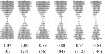
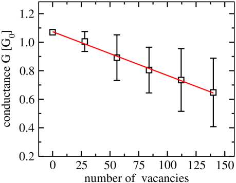
In order to estimate the significance of tip disorder we have therefore prepared a perfect junction as above and then randomly removed atoms from the surface of the electrode in the vicinity of the contact point. The number of silver atoms in the extended molecule region is systematically decreased by removing 28 atoms at randomly chosen surface positions. To maintain coherent transport, the two central atoms were never removed. Every junction geometry with vacancies was generated 500 times, with randomly chosen vacancy positions. For each conformation we computed and subsequently averaged the conductance. The calculations were performed using a principal layer thickness parameter .
Samples of the resulting junction conformations are shown in Fig. 5 with the corresponding averaged conductance value in units of G0, respectively. In addition, the total number of surface vacancies on the current junction geometry is given below the conductance values. Figure 6 shows the resulting conductance values averaged over conformations with equal number of surface impurities. Creating 140 vacancies, which is half of the initial number of atoms, reduces the total conductance by 40% in average. The rapidly increasing size of the error-bars indicates that the change in the conductance depends strongly on their positions.
III.3 Silver Nanoclusters
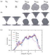
Recent experiments of silver junctionsXie et al. (2004, 2008b) suggest a strong stability of the observed zero-bias conductance in electrochemically grown silver junctions. While this effect was locally explainedXie et al. (2008a) by the selection of specific contact geometries, the overall shape of the silver contacts is likely to vary strongly from one realization of the next. To assess the effect of these large-scale geometric differences, we have prepared locally similar, but globally different junction geometries by placing silver clusters of various size in different orientations on a perfect surface and then contacting the tip of the cluster with an ”ideal” junction. For this purpose we use the optimized cluster geometries from Ref. Shao et al. (2008); Jonathan and Wales (1998), which where generated by Monte Carlo minimization and the modified dynamic lattice search method. Figure 7a shows the top view of the studied silver clusters with 5, 7, 180, 220, and 260 atoms and decahedron (-Dh) core symmetry. As illustrated in Fig. 7b we consider the metal clusters attached to a silver substrate layer of the crystallographic [111] direction. The second electrode is realized by a pyramidal tip on top of the nano-cluster similar to a STM-setup.
We optimized the position of the silver nano-cluster on the substrate using a Metropolis Monte-Carlo technique combined with the semi-empirical Gupta potential for the silver atoms as described above. During the simulation the silver cluster is treated as a rigid body, so only translations and rotations of the cluster are allowed - structural rearrangements insight the cluster are forbidden. The metal cluster surface consists of a set of [111], [110] and [100] facets. The minimum of the potential energy is reached, if the system is arranged such that the largest [111] facet (which is always the largest subsurface in the present cases) and the [111] substrate layer are facing each other. The top electrode is assumed to point directly on one arbitrarily chosen silver atom on the cluster surface.
Figure 7c shows the total transmission function of the clusters Ag5, … , Ag260. The conductance of the systems is given by the average of the transmission over a small interval around the Fermi energy with meV. For the clusters with 5, 7, 180, 220, and 260 atoms we find conductance values of 1.10, 1.08, 1.15, 1.17, and 1.17 G0, respectively, which means, that the conductance is less effected by the size of the nano-cluster and depends more on the point contact to the second electrode. This observation may explain the observed stability of the experiment: While reconstruction of the junction geometry assures the selection of a specific local geometry, the overall conductance depends only very little on the global shape of the clusters forming the contact. This result is also in good agreement with an earlier study E. Bascones et al. (1986) using a simplified model based on random matrix theory.
We also note that an irregular fluctuation of the transmission as a function of energy is observed, which increases with the cluster size. Such fluctuations can be conceptually explained by the interference of the incident electron waves with waves scattered repeatedly in the extended molecule region containing the sliver nano-cluster and the electrode tip. Increasing the cluster size permits scattering processes of increasing order which leads to conductance fluctuations of higher frequency. An analysis of the average energy spacing of the extrema of the transmission (which may be measured by applying a gate voltage) can help to estimate the size of the backscattering region.
III.4 Thermal fluctuations of the conductance of oligophenylene wires
So far we have discussed only mononuclear extended molecule regions. It is well known that the presence of metal-organic interfaces complicates electronic structure and, as a result, electronic transport calculations. We have therefore studied the coherent conductance of phenyle-di-thiol (PDT), a ,,Drosophila” of molecular electronics. Because this molecule was studied extensively in the past Strange et al. (2008); Evers et al. (2004); Kondo et al. (2006); Tomfohr and Sankey (2004); Emberly and Kirczenow (2003); Reed et al. (1997); Varga and Pantelides (2007); Di Ventra et al. (2000), it allows for a comparison of the RLGF approach with experiment and various other levels of theory. We investigate the transmission of oligophenylene molecules of varying lengths, which lend themselves nicely to an investigation of the layer approximation in an organic, semi-conducting system. The structure of the molecules suggests a natural introduction of layers in terms of single phenyl-ring units, similar to the layers introduced by base-pairs in DNAStarikov et al. (2005).
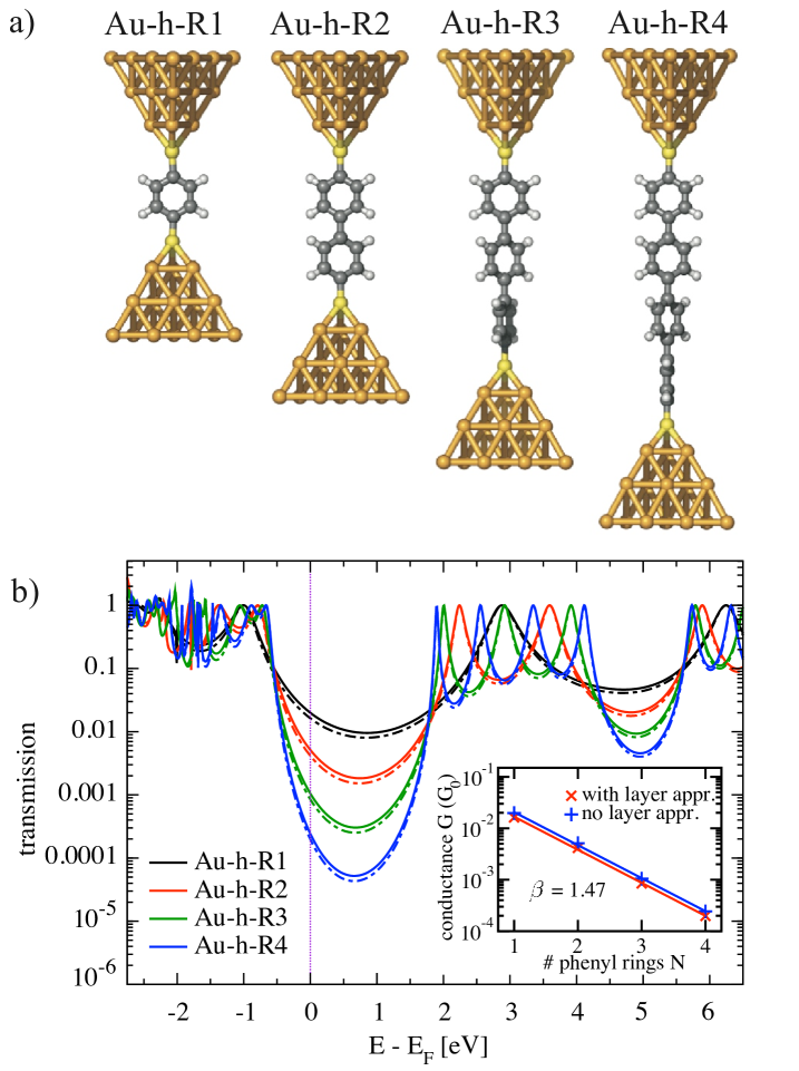
Figure 8a illustrates the oligiphenylene molecules covalently bound to Au19-clusters, using the same notation as for the conformations in Ref. Pauly (2007). The molecule is connected to the Au electrodes at both sides by a symmetric covalent bond of a sulfur atom to three Au atoms. In the literature this bonding situation is referred to as the hollow position Pauly (2007). The electrode clusters where constructed from fcc lattices as above, while the geometry of the phenyl wires was optimized using density functional theory (DFT) in the local density approximation (LDA) Ahlrichs et al. (1989); Wohlthat et al. (2007); Pauly (2007). As can be seen in Fig. 8a there is a non-vanishing tilt-angle between the phenylene-rings, which varies between 33.7 and 34.5 degrees due to the interplay of steric repulsion and -conjugation of adjacent rings. A detailed investigation of the influence of (conjugation induced) tilting on the coherent transport properties in biphenyl-derived dithiols was recently given in Ref. Pauly et al. (2008b).
In Fig. 8b the total transmission is shown as a function of energy for the molecular junctions above, once with (dashed line) and once without the layer approximation (solid line). Due to the neglect of several overlap matrix elements the transmission and conductance obtained with the layer approximation is below the full device transmission (see table 1). The measured conductances of oligophenylene wires with amine end groups indicate even lower conductance values (also given in table 1) which may arise from the differences in the coupling to the electrodes. With increasing length of the phenyl wire the transmission gap decreases from 3.89 eV to 2.56 eV. The equidistant transmission at the Fermi energy of the different molecular wires indicates the correct exponential decrease of the conductance with linear increasing wire length Viljas et al. (2008); Wold et al. (2002); Wakamatsu et al. (2006); Venkataraman et al. (2006). The proportionality of the conductance decay of the oligophenylene wires once with and once without the layer approximation is shown as inset in Fig. 8b. In both cases we obtain a decay coefficient which is close to the experimental value reported in Venkataraman et al. (2006) for amine end groups. Nevertheless, the comparison between theory and experiment remains difficult because of the different end groups used.
Next we investigate the influence of thermally induced molecular vibrations on the coherent transport properties of an Au-h-R4 wire. For the simulation of the dynamics of the system we use of the AMBER 8 molecular dynamics package Case et al. (2005), which employs the well established GAFF-forcefield and a Langevin thermostat method to model temperature. Assuming fixed gold atoms of the electrodes we simulate the evolution of the system at 300 K for 10 ps in time steps of 2 fs. Every 10-th time step a snapshot of the conformation is taken as input for the conductance calculation generating 500 conformations for analysis. For each conformation we calculate the zero-bias conductance. Within the simulation period we find repeated conductance fluctuations by more than an order of magnitude.
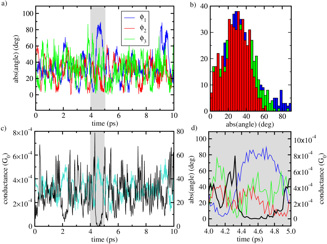
Recent investigations have already focused on the influence of intramolecular vibrations on the conductance Xie et al. (2008a). Here, we find an interesting model system where thermal fluctuations induce large-scale conformational change. The conductance of a conformation correlates highly with its ”planarity”, because the fully planar conformation leads to a strong overlap of the -orbitals, which in turn increases the transmission. However, such planar configurations are forbidden at zero temperature because of steric repulsion of the hydrogen atoms emanating from the rings. Figure 9a shows the fluctuation of the torsion angles , and between the ring-units occurring in Au-h-R4, respectively. All three torsion angles fluctuate strongly around an equilibrium average of 33.9 degrees, which agrees well with the experimentally observed equilibrium value of 34 degrees. The histogram Fig. 9b shows that the outer torsion angles and have slightly broader distributions than , which may be caused by the lower potential energy barrier at the electrodes. The average conductance over 10 ps arises as an average of strongly fluctuating instantaneous values, as illustrated in Figure 9c.
In the course of the the 10 ps simulation we find 6 ”near-planar” configurations of adjacent rings and 2 ”near-planar” conformations of all three rings. To characterize this geometric feature we compute the average of the absolute torsion angles , which has 4 minima (with deg) and 3 maxima (with deg) in the observation period. As illustrated in Fig 9c the conductance has associated minima where is maximal, e. g. at 2.2, 4.3, and 9.4 ps. Correspondingly the highest conductance values are obtained, if is small, e. g. at 4.6, 5.5, and 9.8 ps. This effect is also illustrated in Fig. 9d, which gives a a higher time-resolution of the grey regions of Fig. 9a and 9c. This analysis shows that the experimentally relevant conductance at room temperature arises as an average of thermally excited high-conductance conformations, which are forbidden at zero temperature.
IV Conclusions and Discussion
Most experimental realizations of nanoscale junctions will contain some degree of structural disorder, which is difficult to assess in situ experimentally. The importance of thermal fluctuations on the local geometry was recently modeled for benzene molecular junctions in good agreement with experimental observationAndrews et al. (2008); Cui et al. (2001). Here we use a recursive layer Green’s function approach for the ballistic electronic transport through several disordered nanojunctions.
We have investigated the influence of imperfect contact geometries on the conductance by studying many different possible realizations of silver and gold nanowires. Tilting the junction electrodes up to 60 degrees reduces the conductance by 20%, while twinning the electrodes leaves the conductance nearly unchanged. We found that the introduction of up to 50% surface vacancies leads to only small variates of the ballistic transport properties of silver contacts, as long as the immediate vicinity narrowest point of the junction was not affected. This analysis was supported by a study of the effects of global conformational change in silver junctions for locally conserved junction geometries. Here we find that variations in the global cluster geometry ranging from 5-260 atoms have only a weak effect on the zero-bias conduction of junctions with locally conserved geometry.
Extending earlier work on local fluctuations we have investigated the impact of thermally induced large-scale geometric change on the conductance of oligophenylene wires. Averaging the conductance over 500 conformations obtained from a 10 ps molecular dynamics simulation at room temperature, we find temporal conductance fluctuations of more than an order of magnitude. The average conductance, which agrees well with the experimentally observed valueWold et al. (2002), results from high-conductivity conformations that are sterically unfavorable at zero temperature. The underlying advances in the modeling approach thus permit the detailed characterization of disorder effects, which present in almost all experimental realizations, on the conductance of molecular wires.
Acknowledgements
We thank Gerd Schön for helpful discussions and Fabian Pauly for providing the structural data on the oligophenylens. We thank David J. Wales and Xueguang Shao for the silver nano-cluster conformations studied in this work. We acknowledge financial support by the DFG (grant WE 1863/15-1) and the use of the computational facilities at the Computational Science Center at KIST, Seoul.
V Appendix
V.1 Layer approximation
The key approximation of the recursive-layer Green’s function approach is the division of the quasi one-dimensional device region into ,,principal layers” (see Fig. 1(b)) perpendicular to the current flow Vergés (1999). In the layer-approximation all Hamiltonian overlap matrix elements between atoms which are separated by more than one principal layer are set to zero. Therefore, the full Hamiltonian of the device region has a block-diagonal form, with representing the Hamiltonian of the ,,principal layer” .
| (6) |
This approximation seems natural for a number of systems, e.g. polymers such as DNA, where the matrix elements between neighboring base-pairs decay rapidly with distance. Overlap matrix elements, as well as Hamiltonian matrix elements of localized atom-centered basis sets decay very quickly with the nuclear distance. Once such a set of principal layers is chosen, we can calculate the zero-bias conductance applying a recursive Green’s function method. In the limit of small bias voltages Vergés Vergés (1999) showed for a rectangular lattice of sites, that the conductance can be evaluated by a recursive calculation of the ,,column” Green’s function, starting at the right lead iterating to the leftmost site column of the device region. The knowledge of the charge flux in the contact between the left most column and the left lead is sufficient to evaluate the total current of the system (due to flux conservation). Here we generalize this scheme to a non-rectangular, all-valence electron model to permit efficient material specific conductance calculations in arbitrary junctions. Since molecular wires are ”quasi one-dimensional” by construction, these systems are always naturally dividable into principal layers in the transport direction. The layer width, which interpolates between the full system and single-atom layers, is a free parameter of the approximation, which must be chosen to reflect the properties of the system.
V.2 Recursive layer Green’s function method
Let us in the following denote as layer and the entire left and right electrode fragment, respectively (see Fig. 1(b)). The computation of the Green’s function starts at the rightmost layer of the central region of the system, containing the rightmost device layer and the semi-infinite right lead layer . Its electronic structure is reflected in the retarded Green’s function matrix
| (7) |
which is more conveniently expressed in terms of the layer-self-energies . The self-energy of the right contact can be computed from the retarded surface Green’s function Vergés (1999) as
| (8) | |||||
| (9) |
Here denotes the coupling matrix of the layers and . We can calculate the Green’s function and self-energy of every principal layer recursively, using the relations:
| (10) | |||||
In a layered system, we have chosen the interface such that the velocity operator has non-vanishing terms only for orbitals connecting the left-most electrode layer (layer 0) with orbitals in layer 1. To compute the GF occurring in equation (5) we thus need only the retarded Green’s function of the system comprising layer 0 and layer 1
| (12) |
which is easily computed from the right- and left-lead self energies .
The final ingredient to the calculation is the computation of material-specific electrode Green’s functions for the left and the right reservoir. In order to avoid problems that may arise from an incommensurate decription of the electrodes and the extended molecule, we compute the electrode Green’s functions using the same parametrization of the Hamiltonian. We assume a semi-infinite fcc-lattice with the experimental lattice constant for both electrodes and exploit a recursive relation for the surface Green’s functions of the form Damle et al. (2002); Guinea et al. (1983), where and denote the diagonal and off-diagonal blocks of in the contacts, respectively. This equation is solved iteratively until is converged, which corresponds to the materials-specific surface Green’s function of a semi-infinite system. As in previous studiesXie et al. (2008b); Pauly et al. (2008a), we compute the surface GFs for all sites in a surface layer of two atomic planes.
It is well known that the conductance is very sensitive to interference effects that arise form small atomic displacementRodrigues et al. (2002); Rego et al. (2003). These effects lead to weak oscillations in the total transmission at which are averaged over in most quantum transport measurements at room temperature. To account for this phenomenon we average over a small interval around the Fermi energy , whereas meV to obtain a representative value of the zero-bias conductance for comparison with experiment.
V.3 Extended Hückel-Hamiltonian
In this investigation we have employed extended Hückel theory (EHT), which has been widely used in molecular electronics calculations in the past Samanta et al. (1996); Dalgleish and Kirczenow (2006); Stafford et al. (2007), for the electronic structure calculations, but other semi-empirical methods can be used as well. Excellent semi-empirical parameterizations exists for a wide array of systems, including metals, biomolecules (e.g. DNA) or semiconductors, but the limitations of this approach (e.g. regarding transferability) are also well known. In our calculations we employ a minimal basis set Davidson and Feller (1986) of non-orthogonal Slater type orbitals , including s-, p- and d-wave functions for each atom. In this representation the matrix diagonal elements of the Hamiltonian are approximated by the corresponding orbital ionization potentials, while the off-diagonal elements are chosen as . Here denotes the overlap matrix elements of . The suitable choice of the basis functions permits a fast evaluation of the integrals . The material specific orbital ionization potentials are extracted from experimental data or ab initio calculations. Here we employ a well established parameter set taken from Ref. Muller (2001). This choice of the Hamiltonian parameters is derived form electronic properties, and so it is partially suited for the description of the coherent transport properties of a quantum system. In explorative calculations we found other semi-empirical parameter sets, which have been derived from structural properties and heats of formation (such as PM6), agreed less with prior theory and experiment.
| molecule | (G0) | (G0) | (G0) |
|---|---|---|---|
| R1 | 16.10 | 14.60 | 6.40 |
| R2 | 4.10 | 3.80 | 1.16 |
| R3 | 0.85 | 0.80 | 0.18 |
| R4 | 0.20 | 0.20 | - |
References
- Nitzan and Ratner (2003) A. Nitzan and M. A. Ratner, Science 300, 1384 (2003).
- Kwiatkowski et al. (2008) J. J. Kwiatkowski, J. Nelson, H. Li, J. L. Bredas, W. Wenzel, and C. Lennartz, Phys Chem. Chem. Phys. 10, 1852 – 1858 (2008).
- Heurich et al. (2002) J. Heurich, J. C. Cuevas, W. Wenzel, and G. Schön, Phys. Rev. Lett. 88, 256803 (2002).
- Oetzel et al. (2008) B. Oetzel, M. Preuss, F. Ortmann, K. Hannewald, and F. Bechstedt, Phys. Stat. Sol. (b) 245, 854 (2008).
- Reed et al. (1997) M. A. Reed, C. Zhou, C. J. Muller, T. P. Burgin, and J. M. Tour, Science 278, 252 (1997).
- Cui et al. (2001) X. D. Cui, A. Primak, X. Zarate, J. Tomfohr, O. F. Sankey, A. L. Moore, T. A. Moore, D. Gust, G. Harris, and S. M. Lindsay, Science 294, 571 (2001).
- Scheer et al. (1997) E. Scheer, P. Joyez, D. Esteve, C. Urbina, and M. H. Devoret, Phys. Rev. Lett. 78, 3535 (1997).
- Scheer et al. (1998) E. Scheer, N. Agraït, J. C. Cuevas, A. L. Yeyati, B. Ludoph, A. Martín-Rodero, G. Rubio-Bollinger, J. M. van Ruitenbeek, and C. Urbina, Nature 394, 154 (1998).
- Agrait et al. (2003) N. Agrait, A. L. Yeyati, and J. M. van Ruitenbeek, Phys. Rep. 377, 81 (2003).
- Thygesen and Jacobsen (2003) K. S. Thygesen and K. W. Jacobsen, Phys. Rev. Lett. 91, 146801 (2003).
- Xie et al. (2004) F.-Q. Xie, L. Nittler, C. Obermair, and T. Schimmel, Phys. Rev. Lett. 93, 128303 (2004).
- Tao (2006) N. J. Tao, Nature Nanotechnology 1, 173 (2006).
- Choi et al. (2008) S. H. Choi, B. Kim, and D. Frisbie, Science 320, 1482 (2008).
- Tans et al. (1997) S. J. Tans, M. H. Devoret, H. Dai, A. Thess, R. E. Smalley, L. J. Geerligs, and C. Dekker, Nature 386, 474 (1997).
- Postma et al. (2001) H. W. C. Postma, T. Teepen, Z. Yao, M. Grifoni, and C. Dekker, Science 293, 76 (2001).
- McEuen and Park (2004) P. L. McEuen and J. Y. Park, Mater. Res. Soc. Bull. 29, 272 (2004).
- Rodrigues et al. (2002) V. Rodrigues, J. Bettini, A. R. Rocha, L. G. C. Rego, and D. Ugarte, Phys. Rev. B 65, 153402 (2002).
- Strange et al. (2008) M. Strange, I. S. Kristensen, K. S. Thygesen, and K. W. Jacobsen, J. Chem. Phys. 128, 114714 (2008).
- Evers et al. (2004) F. Evers, F. Weigend, and M. Koentopp, Phys. Rev. B 69, 235411 (2004).
- Andrews et al. (2008) D. Q. Andrews, R. P. V. Duyne, and M. A. Ratner, Nanolett 8, 1120 (2008).
- Pauly et al. (2006) F. Pauly, M. Dreher, J. K. Viljas, M. Häfner, J. C. Cuevas, and P. Nielaba, Phys. Rev. B 74, 235106 (2006).
- Häfner et al. (2008) M. Häfner, J. K. Viljas, D. Frustaglia, F. Pauly, M. Dreher, P. Nielaba, and J. C. Cuevas, Phys. Rev. B 77, 104409 (2008).
- Pauly et al. (2008a) F. Pauly, J. K. Viljas, and J. C. Cuevas, Phys. Rev. B 78, 035315 (2008a).
- Viljas et al. (2008) J. K. Viljas, F. Pauly, and J. C. Cuevas, Phys. Rev. B 77, 155119 (2008).
- Vergés (1999) J. A. Vergés, Comp. Phys. Commun. 118, 71 (1999).
- van Zalinge et al. (2006) H. van Zalinge, A. Bates, D. J. Schiffrin, E. B. Starikov, W. Wenzel, and R. J. Nichols., Angew. Chemie 45, 5499–5502 (2006).
- Xie et al. (2008a) F.-Q. Xie, R. Maul, A. Augenstein, C. Obermair, E. Starikov, G. Schön, T. Schimmel, and W. Wenzel, Nano Lett. 8, 4493 (2008a).
- Novaes et al. (2006) F. D. Novaes, A. J. R. da Silva, E. Z. da Silva, and A. Fazzio, Phys. Rev. Lett. 96, 016104 (2006).
- Rego et al. (2003) L. G. C. Rego, A. R. Rocha, V. Rodrigues, and D. Ugarte, Phys. Rev. B 67, 045412 (2003).
- Jonathan and Wales (1998) J. D. Jonathan and D. Wales, New J. Chem. 22, 733 (1998).
- Shao et al. (2008) X. Shao, X. Yang, and W. Cai, Chem. Phys. Lett. 460, 315 (2008).
- Ledo et al. (2007) A. Ledo, F. Martínez, M. López-Quintela, and J. Rivas, Phys. B: Condens. Matter 398, 273 (2007).
- Ramnani et al. (2007) S. Ramnani, J. Biswal, and S. Sabharwal, Radiat. Phys. Chem. 76, 1290 (2007).
- Heimel et al. (2006) G. Heimel, L. Romaner, J.-L. Brédas, and E. Zojer, Phys. Rev. Lett. 96, 196806 (2006).
- Preuss et al. (2005) M. Preuss, W. G. Schmidt, and F. Bechstedt, Phys. Rev. Lett. 94, 236102 (2005).
- Landauer (1970) R. Landauer, Phil. Mag. 21, 863 (1970).
- Büttiker et al. (1985) M. Büttiker, Y. Imry, R. Landauer, and S. Pinhas, Phys. Rev. B 31, 6207 (1985).
- Damle et al. (2002) P. Damle, A. W. Ghosh, and S. Datta, Chem. Phys. 281, 171 (2002).
- Guang-Can (2006) X. Guang-Can, J. Cluster Science 17, 457 (2006).
- Qian et al. (2006) X. Qian, J. Li, X. Lin, and S. Yip, Phys. Rev. B 73, 035408 (2006).
- Xie et al. (2008b) F.-Q. Xie, R. Maul, S. Brendelberger, C. Obermair, E. B. Starikov, W. Wenzel, G. Schön, and T. Schimmel, App. Phys. Lett. 93, 043103 (2008b).
- Kondo et al. (2006) H. Kondo, H. Kino, J. Nara, T. Ozaki, and T. Ohno, Phys. Rev. B 73, 235323 (2006).
- Tomfohr and Sankey (2004) J. Tomfohr and O. F. Sankey, J. Chem. Phys 120, 1542 (2004).
- Emberly and Kirczenow (2003) E. G. Emberly and G. Kirczenow, Phys. Rev. Lett. 91, 188301 (2003).
- Varga and Pantelides (2007) K. Varga and S. T. Pantelides, Phys. Rev. Lett. 98, 076804 (2007).
- Di Ventra et al. (2000) M. Di Ventra, S. T. Pantelides, and N. D. Lang, Phys. Rev. Lett. 84, 979 (2000).
- Starikov et al. (2005) E. B. Starikov, S. Tanaka, N. Kurita, Y. Sengoku, T. Natsume, and W. Wenzel, Eur. Phys. J. E 18, 437 (2005).
- Pauly (2007) F. Pauly, Ph.D. thesis, Universität Karlsruhe (TH) (2007).
- Ahlrichs et al. (1989) R. Ahlrichs, M. Bär, M. Häser, H. Horn, and C. Kölme, Chem. Phys. Lett. 162, 165 (1989).
- Wohlthat et al. (2007) S. Wohlthat, F. Pauly, J. K. Viljas, J. C. Cuevas, and G. Schön, Phys. Rev. B 76, 075413 (2007).
- Pauly et al. (2008b) F. Pauly, J. K. Viljas, J. C. Cuevas, and G. Schön, Phys. Rev. B 77, 155312 (2008b).
- Wold et al. (2002) D. J. Wold, R. Haag, M. A. Rampi, and C. D. Frisbie, J. Phys. Chem. B 106, 2813 (2002).
- Wakamatsu et al. (2006) S. Wakamatsu, S. Fujii, U. Akiba, and M. Fujihara, Jpn. J. Appl. Phys. 45, 2736 (2006).
- Venkataraman et al. (2006) L. Venkataraman, J. E. Klare, M. S. Hybertsen, and M. L. Steigerwald, Nature 442, 904 (2006).
- Case et al. (2005) D. A. Case, T. E. Cheatham, T. Darden, H. Gohlke, R. Luo, K. M. Merz, A. Onufriev, C. Simmerling, B. Wang, and R. J. Woods, J. Comput. Chem. 26, 1668 (2005).
- Guinea et al. (1983) F. Guinea, C. Tejedor, F. Flores, and E. Louis, Phys. Rev. B 28, 4397 (1983).
- Samanta et al. (1996) M. P. Samanta, W. Tian, S. Datta, J. I. Henderson, and C. P. Kubiak, Phys. Rev. B 53, R7626 (1996).
- Dalgleish and Kirczenow (2006) H. Dalgleish and G. Kirczenow, Phys. Rev. B (Condensed Matter and Materials Physics) 73, 245431 (2006).
- Stafford et al. (2007) C. A. Stafford, D. M. Cardamone, and S. Mazumdar, Nanotechnology 18, 424014 (6pp) (2007).
- Davidson and Feller (1986) E. Davidson and D. Feller, Chemical Reviews 86, 681 (1986).
- E. Bascones et al. (1986) E. Bascones, G. G mez-Santosand J. J. S enz, Phys. Rev. B 57, 2541 (1998).
- Muller (2001) E. Muller, (Edgar.Muller@icma.unil.ch), Tables of Parameters for extended Hückel Calculations, available in YAeHMOP 2.0. (2001).