Tight-binding photonic bands in metallophotonic waveguide networks and flat bands in kagome lattices
Abstract
We propose that we can realize “tight-binding photonic bands” in metallophotonic waveguide networks, where the photonic bound states localized around the crossings of a network form a tight-binding band. The formation of bound states at the crossings is distinct from the conventional bound states at defects or virtual bound states in photonic crystals, but comes from a photonic counterpart of the zero-point states in wave mechanics. Model calculations show that the low-lying photon dispersions are indeed described accurately by the tight-binding model. To exemplify how we can exploit the tight-binding analogy for designing of photonic bands, we propose a “flat photonic band” in the kagome network, in which the photonic flat band is shown to arise with group velocities that can be as small as 1/1000 times the velocity of light in vacuum.
pacs:
42.70.Qs, 41.20.Jb, 42.25.-pPhotonic crystals (PhCs) are interesting because they enable us to control optical properties just as we can manipulate properties of electrons in solids.Pendry (1996) PhCs have attracted both experimentalYablonovitch et al. (1991a); Wanke et al. (1997) and theoreticalJohn (1987); Pendry and MacKinnon (1992); Gersen et al. (2005) interests, and the dramatic developments in the field in fact owe much to the analogies between PhCs and solids. Many phenomena first found in solids have also been found in PhCs, such as the appearance of band gapsYablonovitch (1987); Yablonovitch et al. (1991b), Anderson localization,John (1987); Anderson (1958) modes localized to defects in the band gap frequency,Yablonovitch et al. (1991a) and lights with small group velocities or heavy photons.Gersen et al. (2005)
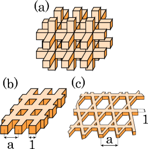
While photonic bands realized in periodically modulated dielectric media have been extensively studied, there should be further avenues that have not been thoroughly explored. In the electronic band structures, there are two opposite approaches well known in solid-state physics: the nearly-free-electron model and the tight-binding model (TBM). While the former is perturbative, the TBM shows a great variety of band structures, and numerous lattices have been analyzed in solid state physics. In this Brief Report we pose a question: can we realize tight-binding photonic bands? Here, we propose a way to realize that. We predict that metallophotonic waveguide networks (MPWNs), where waveguides are joined together to form a network structure as schematically depicted in Fig. 1, should realize the tight-binding photonic bands through an unsuspected “zero-point” localized photonic states. The network is taken to be surrounded by a material into which light cannot penetrate, so that the light is confined inside the network. An obvious material is a metal for a sufficiently smaller frequency than the plasma frequency, such as in the microwave regime. Networks of line-defect waveguides in PhCs may be another possibility, but the detail of the surrounding material is unimportant as long as the confining property and low-loss condition are satisfied.
We note that there exist literatures that propose some ways to realize tight-binding photonic bands for coupled waveguides or cavities in PhCs,Amiri et al. (2006); Stefanou and Modinos (1998); Bayindir et al. (2000) and calculation methods based on the TBM have been successfully applied to these systems.Lidorikis et al. (1998); Albert et al. (2002) However, most tight-binding studies have relied on the introduction of defects, around which a localization mechanism inside the band gap is sought. The MPWN we propose here, by contrast, exploits a different mechanism. The tight-binding photonic bands in MPWNs are shown to arise from the states bound to each crossing of the waveguide, which is a photonic version of the zero-point effect in quantum mechanics and has not been recognized so far. MPWNs thus make it possible to realize tight-binding bands without defects. The concept of the zero-point state turns out to be quite powerful in offering a clear understanding of low-lying eigenmodes in these systems. In terms of structures, three-dimensional MPWNs are similar to the inverted metallophotonic crystals of the woodpile type,Lee et al. (2006) but MPWNs cover a wider class of systems including two-dimensional structures as in Figs. 1(b) and 1(c). In those inverted PhCs, it has been recognized that air-band Bloch modes will localize to the air region. While this localization mechanism will not tell us whether the modes will localize to the crossings as in our results, or at ”arms,” the zero-point localization mechanism tells us that they will localize at the most vacant sites among the large dielectric constant region, namely, crossings due to the zero-point effect. Thus, the zero-point localization mechanism offers further insights into behaviors of eigenmodes than the conventional concept does.
Here, we shall first show that the TBM is indeed a good approximation by taking a two-dimensional square-lattice MPWN as a typical example. To exemplify that we can use the tight-binding photonic bands to design the photonic band structures, we shall next consider metallophotonic waveguide on the kagome network. We shall show that the band structure for the kagome network contains flat bands, which are flat over the entire Brillouin zone with group velocities typically as small as 1/1000 times the velocity of light in vacuum. This amounts to a photonic realization of the “flat-band model” in solid state physics as conceived by Lieb,Lieb (1989) Mielke,Mielke (1993) and Tasaki.Tasaki (1992) Ultra slow light is among keen interests in PhCs,Gersen et al. (2005); Vlasov et al. (2005) which has also been discussed in view of realizing a low-threshold laser. We then conclude that the tight-binding analogy should provide a systematic way to create photonic bands with desired band structures.
Band structure for a square lattice. To demonstrate our basic idea for the tight-binding photonic band, we take the simplest example of a square-lattice network [Fig. 1(b)] for the waveguide. Here, we focus on the TM-polarized mode (i.e., ) in two-dimensional networks. The validity of the TBM that we discuss here, however, can be extended to three-dimensional cases with arbitrary polarizations as mentioned later. While a band calculation for metallophotonic crystals is more complicated than those for PhCs with dielectrics, here we employ a simplified method as follows to extract the essence of the band structure. We assume that the metal that forms the wall of the network can be represented by a medium having a large and negative dielectric constant. Thus, we set the dielectric constant inside the waveguide to be unity, while the dielectric constant outside is taken to be in actual calculations. This should be adequate for describing a metal, at least in the microwave regime, where the metal can be effectively regarded as completely reflective. For shorter wavelengths, e.g., in the optical regime, the loss associated with the metal may not be ignored. A possible way out from the loss in this regime will be to employ line-defect waveguides since there is no loss associated with the material.
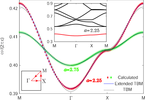
Band structures and eigenmodes have been obtained numerically with a plane-wave expansion methodPendry (1996) for each value of the lattice constant of the network structure, while we set the width of each waveguide to be unity. We take a sufficient number of plane waves (typically 7225) to attain convergence.
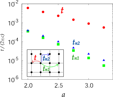
The band structure for the square-lattice network for is shown in the inset of Fig. 2. We then fit the lowest band with the tight-binding band as shown in Fig. 2 for two values of . We can see that the fit is already good for the TBM with nearest-neighbor transfers, while the fit becomes even better when we include the further-neighbor transfers (, in Fig.3). We quantify this by plotting the best-fit nearest-neighbor and further-neighbor transfers against the lattice constant in Fig. 3. Each of the transfers is seen to decrease exponentially with , where further-neighbor transfers decay more rapidly.
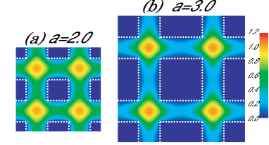
If we look at the eigenmodes, shown for the lowest band in Fig. 4, they are in fact localized around each crossing, with a rapidly decaying tail toward the neighboring junctions. We note that the existence of the bound amplitude localized around each crossing is analogous to the corresponding localized states in quantum mechanics, which exist due to a zero-point effect. Namely, for an electron system in crossed quantum wires, it has been shownSchult et al. (1989) that there exist bound states at the crossing. This comes from the fact that the wavefunction has a smaller zero-point energy at a crossing to form a bound state since the electron is less constrained there than in an arm. Schrödinger’s and Maxwell’s equations for two-dimensional, TM-polarized PhCs are equivalent,Zhukovsky and Gaponenko (2008) so that the results in Schrödinger’s equation can be applied to the present system. When we translate the former to the present system, the lowest bound-state energy should be 0.406 (in units of with the waveguide width ). The center of the tight-binding band (i.e., the on-site energy in the tight-binding fit) in Fig. 2 is , which excellently agrees with the present result.
Such an excellent agreement owes much to the formation of the bound states. By contrast, resonant states, which have intrinsic losses, will couple to extended states to result in significant transfers to distant neighbors, deteriorating the tight-binding picture with near-neighbor transfers. The origins of the losses include the loss in the surrounding material, the out-of-plane energy leakage, and the radiation loss due to a finite size. While the first one may be avoided for metals in the microwave regime and for line-defect waveguides, the latter two losses can degrade the tight-binding fit.
We note that the existence itself of such localized states has been suggested for photonic crystal waveguides. Namely, it has been pointed out that there is a state in the photonic band gap with amplitudes localized around a T junction,Mekis et al. (1996) while a high transmission through a bend in a waveguide is observed for which a possibility for bound states is pointed out.Albert et al. (2002) However, the band structure due to a periodic array of such localized states in a periodic waveguide network has not been explored.
The tight-binding band considered here should emerge in general in MPWNs for arbitrary spatial dimensions and polarizations. Namely, the tight-binding bands emerge from the bound states via the zero-point analog states in MPWNs, which will continue to exist when we consider more complicated structures with arbitrarily polarized electromagnetic fields. Thus, we envisage here that MPWNs should generally accommodate tight-binding photonic bands.
There is a way to achieve tight-binding bands in existing studies employing coupled plasmon modes,Ito and Sakoda (2001) but these bands should be susceptible to disorder in the surface of metals. The present system, on the other hand, should be robust against disorder. It has been known for cavities that a disorder in the surface of a cavity does not significantly decrease the value.Joannopoulos (1999) The robustness comes from the fact that the field resides away from the surface, which also applies to the bound states considered here.
Kagome lattice and a flat band. To show that the present TBM can be a powerful guideline in designing photonic bands, we propose that the photonic band in a kagome network of waveguides [Fig. 1(c)] should contain flat bands. A curious point is that the class of flat bands considered here is totally different from a dispersionless band in the narrow-band (i.e., zero-transfer) limit. The emergence of the flat band, originally considered in solid-state physics by Mielke and by Tasaki, is due to an interference effect inherently connected to the topology of the lattice, and thus the flat band exists no matter how large the transfers between the states at adjacent sites are. For electrons, there has been attempts to realize flat electronic bands in the kagome (a typical Mielke) network of quantum wires.Shiraishi et al. (2001); Coulson (1954) So we pose a question here: can we realize the topologically originated flat photonic bands?
The result in Fig. 5 shows that the lowest three bands have the same forms as in the TBM, where the third photonic band from the bottom is indeed extremely flat, as expected. The width of this band is in fact (for ) in the present normalization, so that light becomes more than 1000 times as slow as light in vacuum. We note that the band becomes flat as an interference effect on the lattice where the nearest-neighbor transfer is primarily at work, so that resonant states with distant transfers would not realize this.
It is intriguing to look at the eigenmodes in the flat band in Fig. 6(a). While they are again localized around the crossing sites, the specialty of the flat band is appreciated if we look at the dependence of the eigenmode on the wave vector . Namely, one hallmark of the flat band à la Mielke is that the part in a Bloch wave function strongly depends on ,Suwa et al. (2003) while the eigenmodes in the zero-transfer limit obviously are not. We can confirm in Fig. 6 that the photonic eigenmode in the flat band indeed depends significantly on in the same manner as in the electron TBM on kagome.
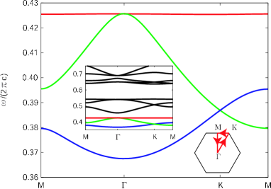
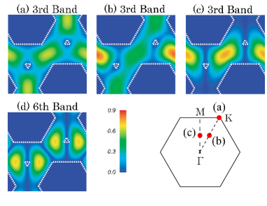
Another notable feature is that there is more than one band which is flat. We can see that the sixth band is also flat as seen in the inset of Fig. 5, with the velocity less than 1/100 times the light in vacuum. If we compare the eigenmodes in the two flat bands in Figs. 6(c) and 6(d), we can see that the sixth band has an eigenmode with an extra node in the unit cell. We can confirm that the two eigenmodes differ only in the nodal structure over the whole Brillouin zone. This implies that these two flat bands originate from different bound states with different symmetries. The existence of more than one bound state is in fact also seen in an electron system at the jointing sites.Schult et al. (1989) Thus the photonic tight-binding bands can accommodate more than one set of bands corresponding to different symmetries in the bound-state modes.
In conclusion, we have considered MPWNs and shown that their band structures can be well captured as the tight-binding photonic bands. This phenomenon can be explained by bound states via the zero-point energy (in the language of Schrödinger’s equation) at the jointing sites. This offers a way to realize tight-binding bands in photonic crystals. To exemplify that the TBM can be exploited as a good guideline in designing photonic bands with desired band structures in MPWNs, we have shown that a kagome network accommodates flat bands with unusually small group velocities. As a prospect there are a vast number of interesting lattice structures for MPWNs to be studied, among which are massless Dirac cones with the “electron” (positive velocity) and “hole” (negative velocity) branches in the honeycomb lattice. Other future problems include the detailed study of loss associated with metals for MPWNs in an optical regime. Quantitative comparisons with other systems and applicational details will also be future problems.
We wish to thank Kazuaki Sakoda and Takafumi Hatano for illuminating discussions.
References
- Pendry (1996) J. Pendry, J. Phys.: Condens. Matter 8, 1085 (1996).
- Yablonovitch et al. (1991a) E. Yablonovitch, T. J. Gmitter, R. D. Meade, A. M. Rappe, K. D. Brommer, and J. D. Joannopoulos, Phys. Rev. Lett. 67, 3380 (1991a).
- Wanke et al. (1997) M. Wanke, O. Lehmann, K. Muller, Q. Wen, and M. Stuke, Science 275, 1284 (1997).
- John (1987) S. John, Phys. Rev. Lett. 58, 2486 (1987).
- Pendry and MacKinnon (1992) J. B. Pendry and A. MacKinnon, Phys. Rev. Lett. 69, 2772 (1992).
- Gersen et al. (2005) H. Gersen, T. J. Karle, R. J. P. Engelen, W. Bogaerts, J. P. Korterik, N. F. van Hulst, T. F. Krauss, and L. Kuipers, Phys. Rev. Lett. 94, 073903 (2005).
- Yablonovitch (1987) E. Yablonovitch, Phys. Rev. Lett. 58, 2059 (1987).
- Yablonovitch et al. (1991b) E. Yablonovitch, T. J. Gmitter, and K. M. Leung, Phys. Rev. Lett. 67, 2295 (1991b).
- Anderson (1958) P. W. Anderson, Phys. Rev. 109, 1492 (1958).
- Amiri et al. (2006) P. Amiri, M. Ranjbaran, K. Mehrany, B. Rashidian, and S. Fathololoumi, Fiber Integr. Opt. 25, 11 (2006).
- Stefanou and Modinos (1998) N. Stefanou and A. Modinos, Phys. Rev. B 57, 12127 (1998).
- Bayindir et al. (2000) M. Bayindir, B. Temelkuran, and E. Ozbay, Phys. Rev. Lett. 84, 2140 (2000).
- Lidorikis et al. (1998) E. Lidorikis, M. M. Sigalas, E. N. Economou, and C. M. Soukoulis, Phys. Rev. Lett. 81, 1405 (1998).
- Albert et al. (2002) J. Albert, C. Jouanin, D. Cassagne, and D. Monge, Opt. Quantum Electron. 34, 251 (2002).
- Lee et al. (2006) J. Lee, C. Kim, Y. Kim, K. Ho, K. Constant, and C. Oh, Appl. Phys. Lett. 88, 181112 (2006).
- Lieb (1989) E. H. Lieb, Phys. Rev. Lett. 62, 1201 (1989).
- Mielke (1993) A. Mielke, Phys. Lett. A 174 443(1993).
- Tasaki (1992) H. Tasaki, Phys. Rev. Lett. 69, 1608 (1992).
- Vlasov et al. (2005) Y. Vlasov, M. O’Boyle, H. Hamann, and S. McNab, Nature 438, 65 (2005).
- Schult et al. (1989) R. L. Schult, D. G. Ravenhall, and H. W. Wyld, Phys. Rev. B 39, 5476 (1989).
- Zhukovsky and Gaponenko (2008) For inhomogeneous systems, Schrödinger’s and Maxwell’s equations are in general different, as in layered dielectrics [see, S. V. Zhukovsky and S. V. Gaponenko, Phys. Rev. E 77, 046602 (2008)]. However, the two equations are equivalent for the present system with metallic walls.
- Mekis et al. (1996) A. Mekis, J. C. Chen, I. Kurland, S. Fan, P. R. Villeneuve, and J. D. Joannopoulos, Phys. Rev. Lett. 77, 3787 (1996).
- Ito and Sakoda (2001) T. Ito and K. Sakoda, Phys. Rev. B 64, 045117 (2001).
- Joannopoulos (1999) J. D. Joannopoulos, Braz. J. Phys. 26, 58 (1996).
- Shiraishi et al. (2001) K. Shiraishi, H. Tamura, and H. Takayanagi, Appl. Phys. Lett. 78, 3702 (2001).
- Coulson (1954) C. Coulson, Proc. Phys. Soc. London A 67, 608 (1954).
- Suwa et al. (2003) Y. Suwa, R. Arita, K. Kuroki, and H. Aoki, Phys. Rev. B 68, 174419 (2003).