00 \jnum00 \jyear2009 \jmonth31 May
Void Growth in BCC Metals Simulated with Molecular Dynamics using the Finnis-Sinclair Potential
Abstract
The process of fracture in ductile metals involves the nucleation, growth,
and linking of voids. This process takes place both at the low rates
involved in typical engineering applications and at the high rates
associated with dynamic fracture processes such as spallation. Here
we study the growth of a void in a single crystal at high rates
using molecular dynamics (MD)
based on Finnis-Sinclair interatomic potentials for the
body-centred cubic (bcc) metals V, Nb, Mo, Ta, and W.
The use of the
Finnis-Sinclair potential enables the study of plasticity associated
with void growth at the atomic level at room temperature and strain
rates from 109/s down to 106/s and systems as large as
128 million atoms. The atomistic systems are
observed to undergo a transition from twinning at the higher end
of this range to dislocation flow at the lower end. We analyze
the simulations for the specific mechanisms of plasticity
associated with void growth as dislocation loops are punched out
to accommodate the growing void. We also analyse the process
of nucleation and growth of voids in simulations of nanocrystalline
Ta expanding at different strain rates.
We comment on differences in the plasticity associated with void
growth in the bcc metals compared to earlier studies in face-centred
cubic (fcc) metals.
keywords:
void growth; molecular dynamics; Finnis-Sinclair potential; body-centred cubic; bcc; dynamic fracture; nanocrystalline tantalum1 Introduction
The process of ductile failure in metals involves the nucleation and growth of voids [1]. Formation of the voids locally relieves the elastic strain energy built up in the material under tension. The voids link up to form the fracture surface, which further relieves the strain energy. Voids nucleate at the weak points in the material when the tensile stress exceeds the material strength at the nucleation site. Often these nucleation sites are at weakly bound inclusions or grain boundary junctions. The material around growing voids undergoes a large deformation (strains of order unity) in order to accommodate the growing void. These large strains require plastic deformation of the matrix material around the void. The interaction of the porosity characteristic of damage and ductile failure and the concomitant matrix plasticity has been studied theoretically using continuum [2, 3, 4, 5, 6], mesoscale [7], and atomistic [8, 9, 10] techniques. Mesoscale [11, 12, 13] and continuum [14, 15] models of void growth and damage have been developed, and yet many aspects remain poorly understood.
One aspect of continued interest is the effect of high strain rates. In engineering applications and mechanical tests the strain rates involved in fracture are low; however, in processes such as projectile penetration and fragmentation ductile fracture occurs under dynamic conditions with very high strain rates [16]. An interesting recent example of a dynamic fracture application is the fragmentation of structures in fusion-class laser systems due to stray light in the enormously powerful lasers [17]. Controlled dynamic fracture experiments can be conducted on a variety of platforms such as gas guns, split Hopkinson bars and lasers. Typically, a plane-fronted compressive wave is generated. It propagates through the sample and reflects off a free surface. The compressive wave become tensile as it reflects off the surface. If the tension exceeds the material strength, fracture occurs. This kind of dynamic fracture is known as spallation.
In this article we study void growth in ductile body-centred cubic (bcc) metals that is associated with dynamic fracture such as spallation. We do not model the wave propagation explicitly [18, 19]; rather we use molecular dynamics (MD) simulation to capture the salient features of the process in a representative volume element that is small compared to the thickness of the rarefaction wave at the spall plane. There are merits to a direct simulation of the wave propagation, but it is challenging in MD to have a simulation sufficiently large in spatial extent and that runs sufficiently long to establish a self-similar wave. Also, the wave form is affected by plastic flow that is initially independent of the growth of small voids since the yield stress is typically significantly below the threshold for nucleation of dislocations at the void surfaces. It is challenging to capture realistic length scales of the dislocation density in MD. So we focus on the case where the release waveform is specified, with a wave front large compared to the voids. We also assume that plastic flow has eliminated much of the shear component of the wave, and we therefore treat the ideal case of equiaxed (hydrostatic) expansion. We consider two cases: one where the voids nucleate from weakly bound inclusions and another where they nucleate from grain boundary junctions in a nanocrystalline system. At low rates a few low-threshold sites can nucleate voids that relieve the tensile stress in a relatively large volume around them; at higher rates, the tensile stress rises to the point that voids nucleate from higher threshold sites before the relief wave from the weakest sites reach them. The result is a higher density of nucleation sites with smaller, stronger nuclei.
Our work here builds on our previous studies of void processes in the dynamic fracture of face-centred cubic (fcc) metals [8]. Using molecular dynamics simulations of fcc copper systems, we have studied the threshold for void nucleation and the subsequent growth and linking processes in nanocrystalline copper [10]. Prismatic dislocation loops punched out to accommodate void growth in an MD simulation were first shown in Ref. [20]. We have shown how varying the stress triaxiality from uniaxial to triaxial tension affects the void morphology and plasticity during growth [21, 22, 23]. We have also examined how voids interact with each other as they transition from a regime of independent growth through the beginning of the coalescence process in which neighbouring voids expand more rapidly toward each other [24, 25].
Here we extend the investigations to bcc metals for several reasons. The higher Peierls barrier for dislocation motion in bcc metals leads to some interesting differences in the mechanisms active in the plastic zone surrounding a void. Also, the bcc dislocations are not split into partials, so the dislocation dynamics is not affected by stacking faults as it is in the fcc case. The behaviour of nanocrystalline bcc metals, including their ductility and fracture, is of current interest [26, 27]. The generation of copious debris has been reported in MD simulations of dislocation motion in bcc metals [28], and it is interesting to see whether such a process plays are role in bcc void growth. Furthermore, bcc metals are known to be prone to twinning at high rate deformation [29], and the role of twinning in void growth has not been explored. A considerable quantity of experimental data on spallation in the bcc metal tantalum is available [30]. Most continuum models of damage do not explicitly account for the lattice structure. The lattice structure only matters insofar as it affects the yield surface [14, 15]. Marked differences observed in the behaviour of voids in bcc and fcc metals then points to new directions for constitutive model development and validation experiments at large laser facilities and/or fourth generation light sources.
We are writing this article as part of a commemoration of the twenty-fifth anniversary of the publication of the Finnis-Sinclair potential [31]. Finnis-Sinclair potentials have proved to be extremely valuable for the study of plasticity at the atomistic level. Based on the physics of electronic structure at the level of the second moment approximation to tight-binding theory [32], they provide a robust description of the bonding physics. At the same time they neglect much of the rococo detail of mixed nearly-free-electron and covalent bonding characteristic of transitions metals that is captured by higher-moment contributions and angular forces. As a result of this approximation, they are computationally efficient, many times less expensive than fourth-moment bond order potentials [33, 34, 35] and Model Generalised Pseudopotential Theory interatomic potentials [36, 37]. This reduction in computational overhead facilitates the simulation of reasonably large system sizes in a way that captures the principal features of the physics relevant to plasticity. It permits relatively quick exploration of large parameter spaces, in some cases suggesting the use of more expensive potentials to determine specific details.
As an extreme example of the horizons opened by these inexpensive and robust potentials, we recently used an aluminium-copper Finnis-Sinclair potential [38] to simulate flows of up to 62.5 billion () atoms for over a nanosecond in order to capture both atomic level phenomena and micron-scale hydrodynamic effects in a complex fluid flow [39]. It was also shown how to implement a ‘onepass’ time integrator that further sped up Finnis-Sinclair simulations by nearly a factor of two, achieving an average performance of 104 Tflop/s in a full simulation. One continuous 2D simulation required 1800 CPU-years, the largest continuous computer simulation ever to the best of our knowledge. This simulation was restarted and ultimately ran for over 2800 CPU-years. The 3D simulation, although not reported yet, took considerably more computer resources. The ability to evolve a cubic micron of atoms for over a nanosecond of simulated time simply would not have been possible with more expensive potentials, nor would it have been worthwhile with less reliable potentials. The simulations we report here are more modest in size and computer requirements with no more than 128 million atoms, but they are enabled by the same advantageous features of the Finnis-Sinclair potentials.
The article is organized as follows. The simulation methods are presented in Section 2. The single crystal simulations differ somewhat from the nanocrystalline simulations, and the details of both series of simulations are described. In Section 3 the techniques used to analyse the large-scale simulations are presented, including the centrosymmetry analysis used for the dislocations and the orientation analysis used for the nanocrystalline deformation. Section 4 describes the stress-strain behaviour of the metals under tension as void growth commences. Section 5 describes the process of dislocation nucleation and glide as the matrix material surrounding the void deforms plastically to accommodate the expanding void. In Section 6 the results of the simulations of void growth in bcc metals are compared to our prior findings for void growth in fcc metals. Section 7 describes the nucleation and growth of voids in nanocrystalline Ta. Finally, our conclusions are presented in Section 8.
2 Simulation Methods
We have conducted the void simulations with the FEMD code, a hybrid finite element (FEM) and MD code for distributed memory supercomputers [40, 41], running in pure molecular dynamics mode. We have used the Finnis-Sinclair potentials [31] with the Ackland-Thetford core correction [42] for the bcc transition metals V, Nb, Mo, Ta, and W. We report simulations of void growth in single crystal metals as well as void nucleation and growth in nanocrystalline Ta. The simulations differed somewhat in the two cases, as described below.
We have also used FEMD to simulate void growth with the part of the lattice near the void represented with MD and the periphery represented with FEM. This approach is similar to the technique used by Marian et al. [43]. The advantage of the hybrid MD/FEM technique is to reduce the computational cost of the large volume of the system that is just elastic. We do not report the results of those simulations here.
2.1 Single Crystal Void Growth Simulation
The single crystal simulations begin with the simulation box filled with a single crystal of the transition metal with a pre-existing void in the centre. The simulation box is expanded at a fixed rate, putting the material under tension, and the void response is monitored. The basic elements of this void simulation technique were introduced by Belak [9]. Specifically, we use a cubic simulation box with periodic boundary conditions with an atomic configuration in a single crystal bcc lattice, unless noted otherwise. A crystal lattice with unit cells was constructed and then all of the atoms were removed inside a spherical void at the centre of the simulation box with radius equal to one tenth of the simulation box size. After the void was formed, 430 195 atoms remain in the box. In some cases a simulation with unit cells and 1 991 622 atoms was used. We have also run a series of simulations with unit cells with a total of 127 463 891 atoms. It will be noted below when these 2-million-atom and 128-million-atom simulations were used. The lattice was oriented with the crystal 100 directions aligned with the simulation box 100 directions. The simulations were carried out starting with the atoms thermalised at room temperature (300K) and zero pressure. The system was thermalised using velocity renormalisation every 100 time steps on the system with the void, and the simulation box was scaled to zero pressure. The actual initial size of the box depends on the zero pressure lattice constant for the metal: Å, Å, Å, Å, and Å.
To simulate void growth in release wave conditions, we focus on a representative volume element that is expanding at a high rate. The simulation box is made to expand at the specified strain rate equally in all three dimensions. We use the technique of Parrinello and Rahman [44], writing the atomic coordinates in terms of a metric times scaled coordinates that take on values in the unit cube:
| (1) |
where the Greek indices indicate spatial dimensions and lower case Latin indices indicate atom number. The metric is increased at a specified true strain rate. The use of uniformly scaled coordinates prevents shock wave formation that would occur if the expansion were driven by tractions on the exterior of the simulation box.
The equations of motion () were integrated using a velocity Verlet integrator [45]. The time step was 3 fs for tantalum, and scaled for the other metals according to the ratio of the lattice constant to the speed of sound. No thermostat was used during the box expansion. In practice the temperature dropped by 20K during the elastic phase of the expansion and then increased by a few hundred degrees during the plastic flow.
2.2 Nanocrystalline Ta Void Simulation
In the case of nanocrystalline Ta the basic technique was the same: a simulation box with periodic boundary conditions was expanded at a fixed strain rate. All three dimensions were expanded equally. The initial configuration of the atoms was the principal difference. A fully dense nanoscale polycrystalline Ta system consisting of 16 384 000 atoms was used as the initial configuration. The nanocrystalline configuration was produced in the simulations of Streitz et al. [46], in which molten Ta was compressed at a high strain rate until it solidified. These simulations were very intensive computationally [47]. We quenched this system down to low temperature and expanded the box until the pressure was approximately zero. We then equilibrated the system to a temperature of 300K and a pressure of 2.55 GPa using velocity renormalisation and rescaling the box [44]. In prior work we have also studied the behaviour of this system under shear deformation [48].
The Finnis-Sinclair potentials are very efficient computationally. Most of the half-million-atom simulations were sufficiently inexpensive to be conducted on a single processor. The larger simulations were run on supercomputers. A 16-million Ta atom configuration on 16 nodes (128 processors) of the Atlas supercomputer at LLNL [49] took an average of 1.3 seconds per time step including all I/O and on-the-fly dislocation and orientation analyses. The largest simulation took an average of 0.24 seconds per time step for 128 million Mo atoms on 512 nodes (4096 processors) of Atlas even though there was a load imbalance across the processors due to the voided region. In all of the simulations we have used a uniform Cartesian spatial domain decomposition.
3 Analysis Methods
Molecular dynamics produces a different spatial configuration of the atoms at each time step. The simulations reported here contain millions of atoms. Much of the information in the atomic coordinates is irrelevant to an analysis of the mechanisms of void growth and plasticity. A reduction of these data to a more manageable form is needed, and it is preferable to effect that reduction as the code runs, on the fly, so that only a subset of the coordinates need be written to disk. The reduction saves disk space, code execution time (the write time can be significant), and analysis time (the time to read the irrelevant data into an analysis routine is also significant).
3.1 Dislocation Identification
The centrosymmetry deviation has proved to be an effective means of finding dislocations. Introduced by Kelchner et al. [50] for dislocation analysis in molecular statics calculations for fcc crystals, we extended it for molecular dynamics at finite temperature [20]. The basic algorithm of calculating the mean-square deviation from centrosymmetry at atom , ,
| (2) |
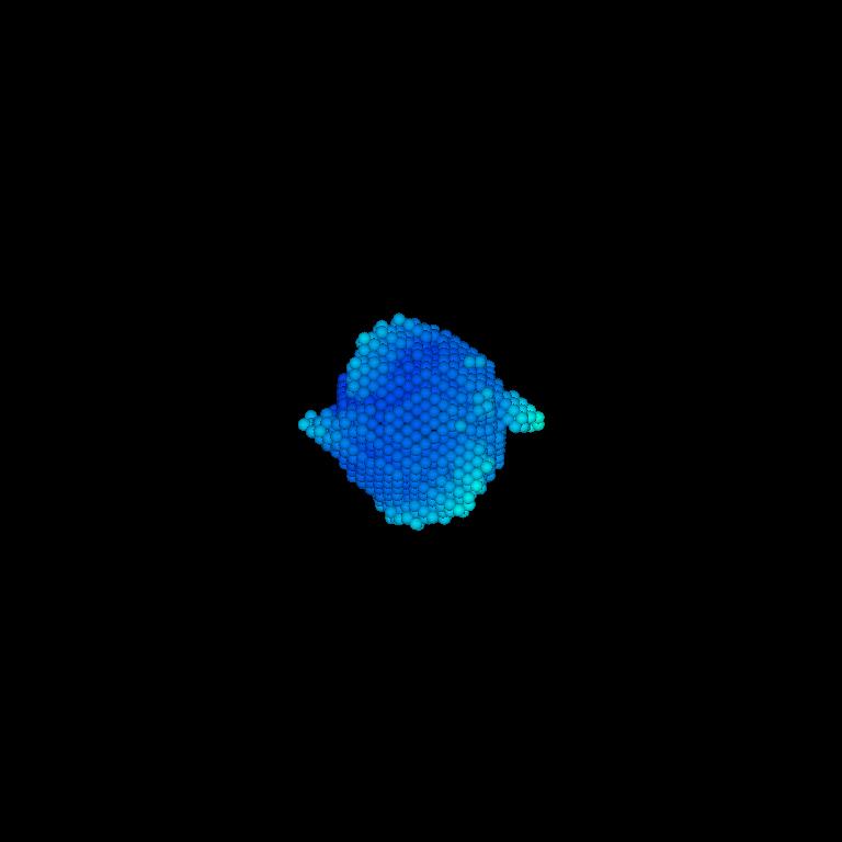
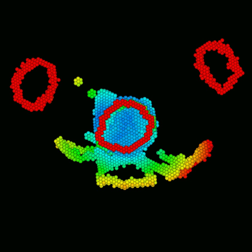
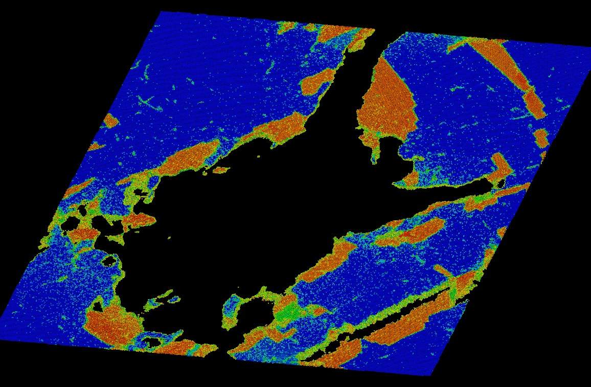
provides a structure-based determination of defects that is fairly insensitive to temperature, even as originally formulated [50] where the displacement is with respect to the central atom . The pairs are formed by matching each neighbour atom with the atom most nearly centrosymmetric to it with respect to the atom . We assign each atom uniquely to a pair, pairing the nearest neighbour first and continuing in order of proximity to atom . Determining defect locations by structure rather than atomic energies [51, 52] is less sensitive to thermal noise. For moderate temperatures (), the is even less sensitive to temperature if the displacements are taken with respect to the centre of mass of the neighbour cluster rather that with respect to atom [20]. Then large values of are indicative of defects such as dislocation cores and stacking faults,111Summing just the three pairs with the lowest gives a variant of centrosymmetry deviation that detects the fcc dislocation cores but not the stacking faults. and plotting those atoms with greater than a threshold value provides a means of visualising the dislocation structure, as depicted in Fig. 1.
For fcc metals, it works well to sum over the six pairs that correspond to the 12 nearest neighbours in the perfect fcc lattice. For bcc metals, we sum over the seven pairs that correspond to the first and second neighbour shells in the perfect bcc lattice. This choice has proved to be less noisy than just summing over the four pairs suggested by the first neighbour shell. Similarly, in silicon the centrosymmetry deviation is naturally defined by the sum over six pairs skipping the four nearest neighbours, effectively defining on an fcc sublattice and ignoring the non-centrosymmetric nearest neighbours. For the bcc visualisations below, we sum seven pairs. The centrosymmetry deviation is determined from differences in atomic positions, so it scales with the nearest neighbour spacing. It is possible to eliminate this material dependence with a rescaling of the displacements by the lattice constant.
3.2 Orientation Identification
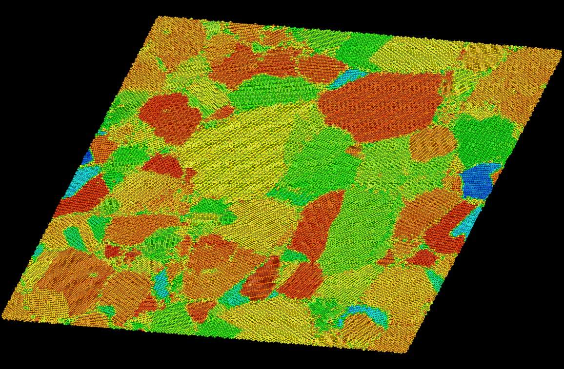
In the case of the nanocrystalline simulations it is also useful to have a means of determining the local lattice orientation. The orientation provides a way to tell grains apart. Furthermore changes in orientation indicate plastic deformation by dislocation, grain rotation and twinning. We have recently introduced a technique to determine the lattice orientation on the fly during a simulation, writing it in the form of a quaternion to enable further analysis, as described in Ref. [48]. We direct the reader to that reference for the details of the technique, and here limit the discussion to a brief comment about quaternions. Lattice orientation like other rigid body rotations is specified by three numbers such as the Euler angles [53]. Quaternions provide another way to describe the orientation. A quaternion may be expressed as a 4-vector with the constraint that for unit quaternions. Quaternions obey multiplication rules appropriate for rotations; i.e. they form a representation of the rotation group SO(3). Unlike the Euler angles they provide a parameterisation of the orientation of a rigid body that is free from coordinate singularities [54, 55, 45]. The visualisation of orientation is facilitated using a colouring that maps the three independent parameters, say to the intensities of red, green, and blue [48].
4 Stress-Strain Response
One of the first quantities to study in dynamic fracture is the stress-strain response. In theory it forms the basis for constitutive models of void growth and damage. In experiment the principal features of this response can be obtained from surface velocity measurements in dynamic experiments using techniques like Velocity Interferometer System for Any Reflector (VISAR). The quantity most often reported to quantify dynamic fracture is the spall strength, a measure of the tensile stress needed for spallation determined from the pull-back part of the surface velocity (VISAR) curve [57]. The MD simulations provide a complete stress-strain curve for the sample, and the peak tensile stress can be compared with experimental spall strength measurements.
We have computed the stress in the MD simulation using the virial expression:
| (3) |
The first term in the stress tensor is the kinetic contribution of atoms denoted with and having masses and velocities . The second term, a microscopic virial potential stress, consists of sums of interatomic forces of atom pairs with corresponding interatomic distances . The indices and denote the atoms, and the indices and denote the Cartesian directions. The thermal stress is included, although in practice it makes only a minor contribution to the changes in stress during the simulated deformation. For a recent discussion of stress calculations in atomistic systems see Ref. [58]. The total system volume is given by . It includes the volume of the void, so the actual stress in the material is greater in magnitude than the value reported. For elastically isotropic continua the stress tensor at point varies around a spherical void of radius subjected to a (negative) pressure according to the form
| (4) |
where is the radial unit vector [59]. The stress field for more general cases can be determined using Eshelby’s techniques [60]. In any case, the stress varies in the vicinity of the void. The stress value we report should be considered an effective stress for the representative volume element containing the void, averaging over these variations.
The stress-strain curves for the group VA bcc transition metals (V, Nb, Ta) and VIA bcc transition metals (Mo and W) are shown in Fig. 2. In each case the simulation box was expanded at a specific true strain rate, expanding the three dimensions equally. The mean stress, , is plotted as a function of the true strain , where and are the current and zero-strain box sizes, respectively. Stress is plotted using the engineering convention that positive stress corresponds to tension. The stress-strain curves at lower strain rates are terminated earlier than at higher strain rates to limit the computational expense which scales as one over the strain rate. A simulation at /s is 1000 times as expensive as a simulation at /s, for the same total simulated time.
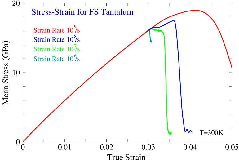
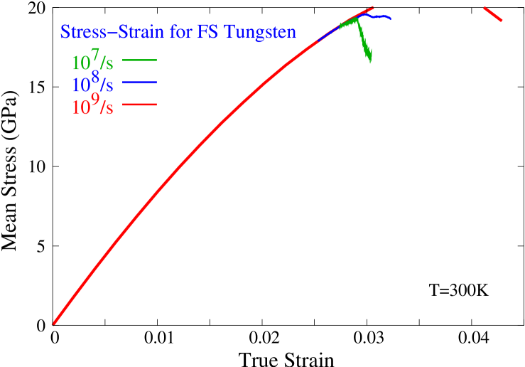
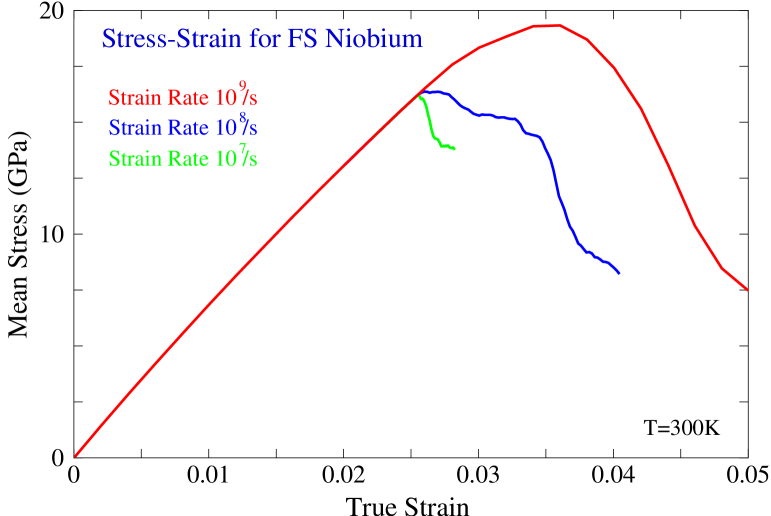
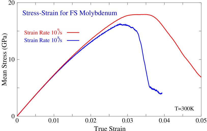
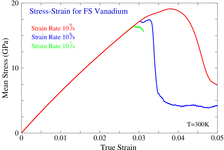
In each case the stress-strain curve shows a smooth regime from zero strain up to a strain of about 0.03. This smooth response is indicative of elastic behavior in which the lattice stretches but no dislocations are formed. The curves are lower than a straight-line extrapolation from zero strain due to the non-linearity of the interatomic potentials. At some point the stress becomes large enough that dislocations nucleate from the surface of the void. The details of this process are described below. The dislocations leave a step on the void surface, expanding the volume of the void and reducing the tensile stress in the material. This reduction takes place smoothly as the dislocation loop is punched out and propagates away from the void. When the void growth rate is high enough that the rate of increase of the void volume matches and then exceeds the rate of increase of the simulation box volume, the mean stress peaks and then decreases. At the highest strain rate, /s, the peak is rounded due to inertial effects. Time is needed for the release wave to propagate through the box so that the stress reduction registers. For a box size of roughly 25 nm and a wave velocity of 5000 m/s, the wave transit time is 5 ps, during which time the box strain increments by 0.005 at /s. So there is a smoothing of the stress-strain curve for /s at this level. The sound velocity also limits the mechanisms of plastic relaxation, dislocation, twinning and fracture, also contributing to the rounded peaks. At strain rates of /s and less this effect is much less significant, so the peaks are sharper. At the lower strain rates, the peak stress is essentially at the yield point; once the void surface has yielded, the void is able to grow at a rate faster than the box is expanding. At higher rates, a peak stress higher than the yield stress is observed. The yield and peak stresses are given in Table 1. For comparison, the yield point in copper was found to be less, about 6 GPa [21].
| Metal | /s | /s | /s | /s |
|---|---|---|---|---|
| V | 16.48 | 17.24 (17.41) | 17.96 (19.11) | |
| Nb | 16.22 | 16.41 (16.46) | 17.65 (19.42) | |
| Mo | 16.13 (16.17) | 17.42 (18.13) | ||
| Ta | 16.13 | 16.36 | 16.51 (17.47) | 17.80 (18.99) |
| W | 19.20 | 19.52 | 20.17 (20.66) |
In some cases the stress-strain curve drops precipitously to a low value of stress; cf. tantalum /s, /s, and vanadium /s. In these cases the system twinned and then cracked along a twin boundary. The crack is able to relieve a large amount of tension rapidly, accounting for the precipitous drop in stress.
4.1 Strain Rate Dependence
Deformation processes such as void growth are strain rate dependent if one or more of the mechanisms sets a time scale. In dislocation motion the time scale can be set by a nucleation or multiplication process in which some incubation time is needed to generate the dislocations needed for plastic flow. In some cases the rate dependence arises because the mechanism is thermally activated, in which case the process is temperature dependent as well, and the use of a finite temperature molecular dynamics simulation (as opposed to molecular statics) is important.
4.2 Comparison with Experiment
Kanel and coworkers have studied the strain rate dependence of the spall strength of Mo [61], and it is interesting to compare their data to the MD results, with the caveat that the comparison is not precise. Their work used a flyer-plate and ablation drives to initiate spallation in Mo single crystals, deformed single crystals, and polycrystals. They considered single crystals aligned in different high-symmetry orientations with respect to the wave. They found that in each case the spall strength increased with strain rate like with an exponent . The deformed single crystals and polycrystals exhibited lower spall strengths than the undeformed single crystals. The single crystal spall strength only had a weak dependence on orientation. The exponent of 0.3 corresponds to a two-fold increase in the spall strength for every factor of 10 increase in the strain rate.
For the 100 single crystal Mo, they found spall strengths ranging from 3.3 GPa at /s to 13.53 GPa at /s [61], so . Accounting for the relationship between the volumetric strain rate and the linear strain rate, , this predicts a spall strength of at a strain rate of /s. The spall strength includes a shear stress contribution that is absent from the MD result. The rate-dependent yield stress of Mo is not known. It is expected to be significantly higher than the ambient yield stress. For comparison purposes, an upper limit is that the material does not yield prior to spall, so that the release wave is pure uniaxial strain. This approximation, where are the Mo elastic constants, gives a mean stress at spall of 30 GPa at /s. This extrapolation from the experimental data is about twice the MD result for the peak stress at /s (16.1 GPa at ). This level of agreement with the experimental results may be reasonable given the somewhat ill-defined nature of the spall strength, but it is not great. Also the rate dependence is different: the MD results do not show a doubling of the peak stress when the strain rate is increased 10. The strain-rate scaling for MD simulations of void growth in copper is much closer to the Kanel scaling [21].
4.3 Void Volume
Void growth is driven by the relaxation of the tensile stress in the material surrounding the void. The greater the volume of the void, the less the matrix material needs to stretch to fill the simulation box. It is interesting to consider how the void volume changes with time during the simulation. We have developed techniques to detect the void surface atoms and use them to calculate the volume of the void, as well as other quantities that we do not consider here such as the surface area and the shape as expressed in multipole moments [23]. This analysis is done on the fly as the simulation runs to reduce I/O to the disk. The results for the void volume as a function of time in Ta and Mo are shown in Fig. 3.
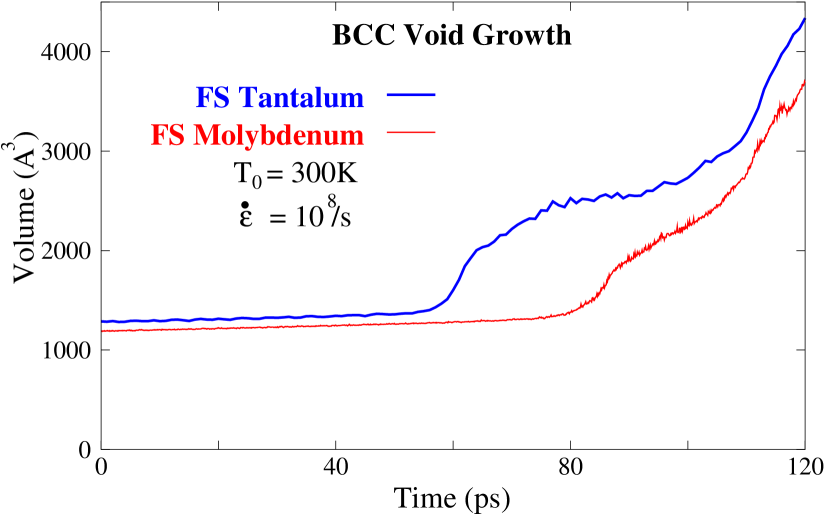
In the plot the curves begin with the elastic regime in which the void is growing slightly as the metal stretches under the applied tension. Much of the elastic regime has taken place before the offset zero of time in the plot. Once plasticity begins, the voids grow rapidly in bursts separated by more quiescent periods. This punctuated growth corresponds to processes in the dislocation nucleation that are explored below. The relative magnitude of the steps in the void growth is larger for these nanoscale voids that it would be for larger voids since the ratio of the change in volume from the emission of a dislocation loop to the void volume goes like , the ratio of the Burgers vector to the void radius, the relative change is most important for nanoscale voids.
While the void volume is not currently measurable in dynamic experiments, in principle the void size distribution could be measured using small-angle x-ray scattering (SAXS) provided a sufficiently intense x-ray source were available. The Linear Coherent Light Source (LCLS) and other fourth generation light sources may provide such the requisite intensity in the near future. Thus far, a proof of principle SAXS measurement has been made in a static experiment on recovered, incipiently spalled titanium at the Advanced Photon Source [62]. Also, tomography has been used to map the locations and sizes of voids under static conditions also using recovered, incipiently spalled samples [63]. Because of the need for x-rays from multiple lines of sight, tomography during dynamic fracture is more challenging but not completely out of the question.
5 Dislocations
The material surrounding the void must deform plastically in order for significant void growth to take place. The traditional assumption in damage modelling is that the stress surrounding the void increases to the yield strength of the material and dislocations flow and multiply according to the laws of continuum plasticity (see for example Ch. 5 of Hill [14]). In this picture the plasticity initiates in the vicinity of the void surface and the plastic zone grows outward as the void grows. Hill estimates the size of the plastic zone after significant void growth as , where is the Young’s modulus and is the yield stress [14]. This model assumes that there are sufficiently many dislocation sources near the void so that material initially within a fraction of the void radius of the surface obeys continuum plasticity.
In modelling the high-rate damage and fracture processes, we have taken a different view. The initial void (or inclusion) may be small compared to the length scale of the dislocation network. In that case the prismatic dislocation flux needed for the void growth does not flow from the matrix, but it is emitted from the void surface. In our single crystal simulations, there are no dislocations initially, so they must nucleate somewhere, and they are observed to nucleate at the void surface in a process that is very similar to how loops were generated in the classic experiments of Mitchell [64] in which hard inclusions punched out dislocation loops in the transparent silver chloride matrix due to stress build up as the temperature changed. The nucleation of dislocations from the void surface requires higher stresses than typical yield stresses, but as we saw above, the spall strength at high strain rates is also very high so the driving stresses are available.
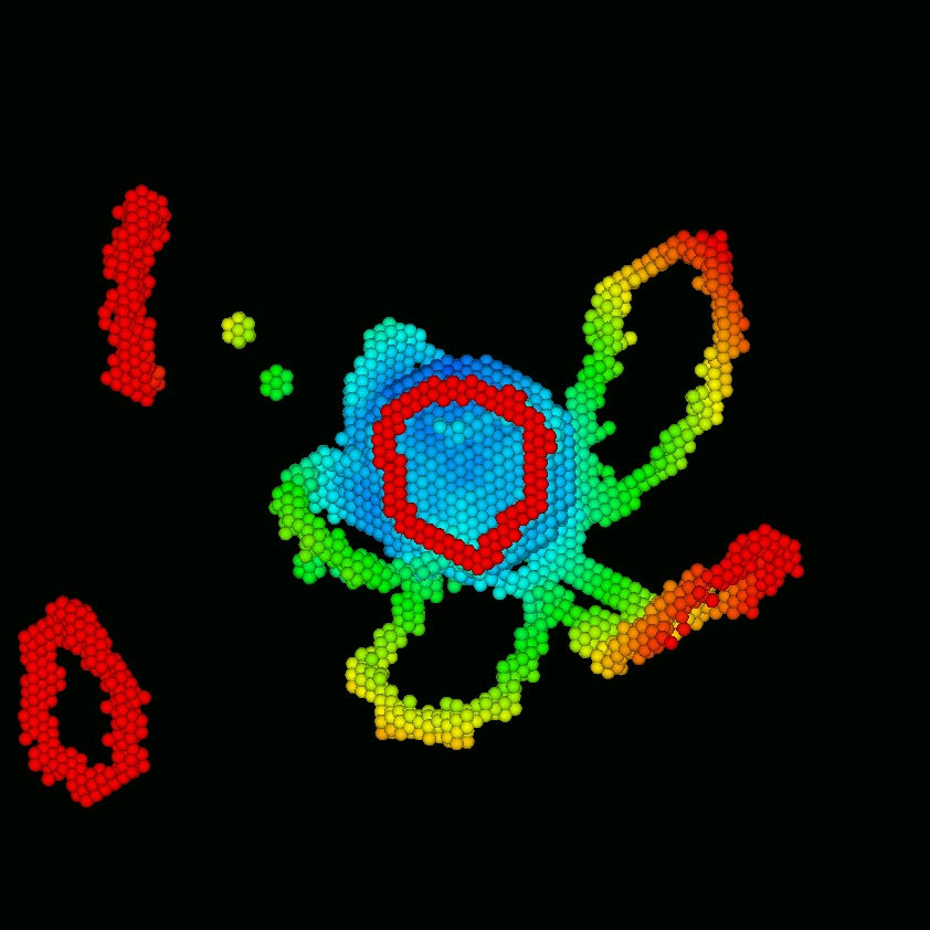
We have used the centrosymmetry deviation analysis to identify dislocations that are generated as the material surrounding the void deforms plastically to accommodate the growing void. A series of snapshots of the dislocations in the material surrounding a void growing in Mo is shown in Fig. 4. As explained above, only atoms at defective lattice sites are shown. Dislocation loops consisting of full dislocations are seen being punched out by the growing void. In Fig. 4 each prismatic loop consists of an edge dislocation surrounding a platelet of interstitial atoms, effectively transporting those atoms away from the void. If the area of the loop is , the volume of atoms is , where is the magnitude of the Burgers vector (2.73Å in Mo). This volume is the amount by which the void grows from before the loop emission once the loop is in the far field. The loops are prismatic in character here since the stress is essentially hydrostatic. Were a background shear stress present, shear loops would be observed [21], but it is still the prismatic component of the loops that leads to an increase in the void volume [8]. Plastic flow prior to void growth limits the shear stress in any case.
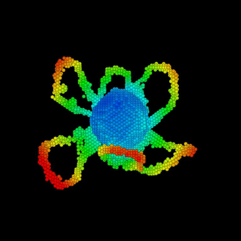
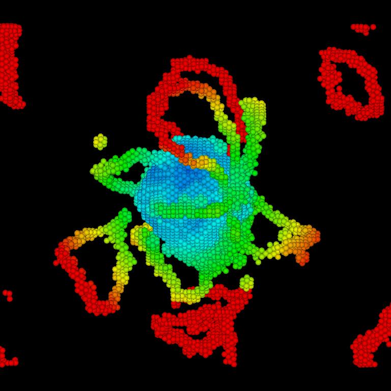
In Fig. 4 a small cluster of atoms appears in the visualisation to the upper left of the void. This cluster consists of atoms surrounding a vacancy created by dislocation climb. The cluster shows up in the visualisation because the atom missing at the vacancy means one of the neighbours is poorly paired in the centrosymmetry deviation, giving a value above the threshold. The dislocation can climb to expand or reduce the size of the loop, leaving a point defect behind. Typically a few of these defects are observed in each void growth simulation. This situation is quite different from the massive amounts of debris formed in the simulations of single dislocation glide reported in Ref. [28]. In that work approximately straight screw dislocations gliding in a specific direction were observed to leave large clusters of vacancies and interstitials behind. The debris formation was attributed to cross-kink formation. Here the dislocations are edge dislocations, at least once they are free of the void, and they are not gliding in a special direction so there is no cross-kink competition. Relatively little debris is formed.
5.1 Prismatic Loop Geometry
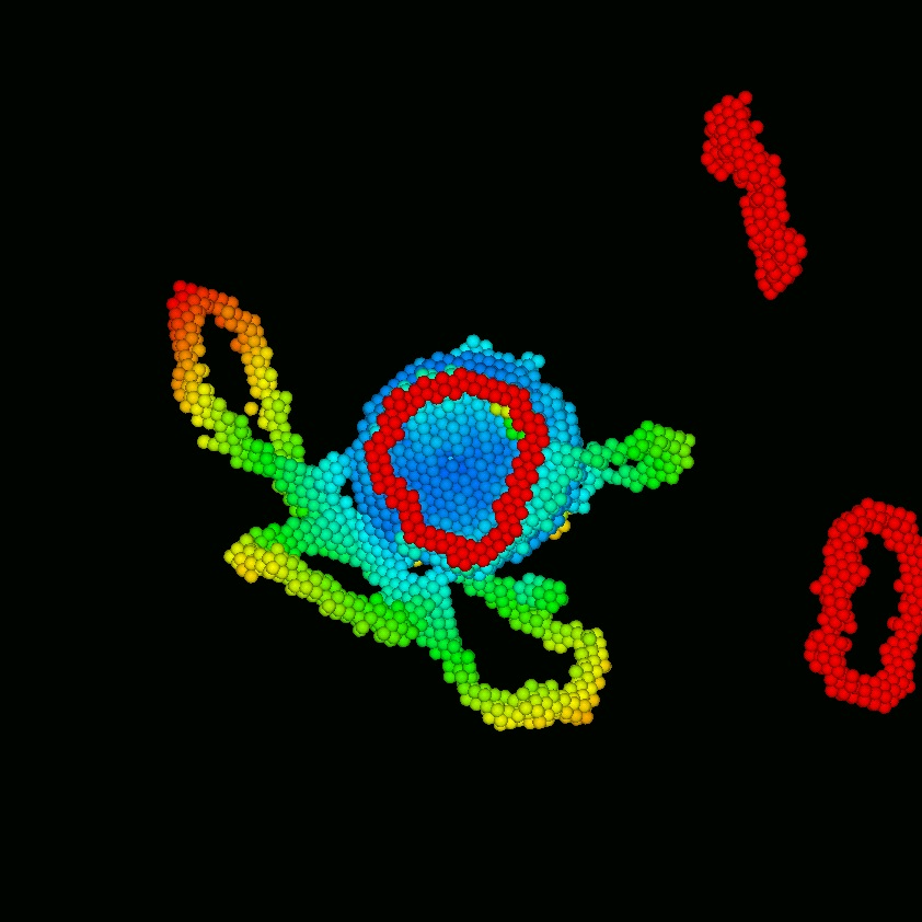
Dislocation loops emitted from the void are shown in Fig. 5. The three panels of the figure show different views of the same dislocation configuration punched out from a growing void, in each case looking down a different 111 line to the centre of the void in Mo. The Burgers vectors of the dislocations are 111, as expected in bcc metals. It can be seen that the prismatic dislocation loops are roughly circular in shape matching the spherical shape of the void. Their size is a bit smaller than the void, and each loop is propagating on a 111 glide cylinder that is concentric with the void. For a spherical inclusion or void in an elastically isotropic medium in pure hydrostatic tension in the far field (cf. the stress field (4)), it is well known that the resolved shear stress at the surface of the void is greatest at from the centre line of the glide cylinder [65]. A dislocation loop that nucleates at this point of maximum resolved shear stress has a radius related to that of the void
| (5) |
With the small voids it is difficult to test this relationship very precisely, but it is approximately obeyed and the loops are observed to increase in size as the void grows.
5.2 Dislocation Nucleation
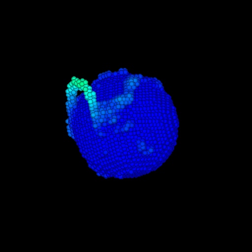
The mechanism of dislocation nucleation during void growth in bcc metals is also interesting, and it differs in some significant ways from the nucleation process in fcc metals. For the purposes of this discussion we consider the nucleation process to include everything from the beginning of dislocation-like fluctuations on the surface of the void through the punch-out process to the point that the prismatic loop has separated from the void. In many of our bcc simulations that nucleation process is well defined–once the leading segment of the loop has glided a few void diameters from the void, the rest of the loop has separated from the void and disentangled itself from the other dislocations. The initial stages of dislocation punch out are shown in Fig. 6. The first panel (Fig. 6a) shows a fluctuation on the surface of the void as loop nucleation begins. The second panel (Fig. 6b) shows a segment of the dislocation loop extending from the surface of the void. The other panels (Fig. 6c-d) show further progression of the loop nucleation. These snapshots are from a 2 million atom MD simulation of Ta void growth at a strain rate of /s. We have changed the simulation size for the nucleation study since the 7 nm void in the larger simulation shows the details of the nucleation process more clearly than the 4 nm voids in the smaller simulations.
It is interesting to note that the dislocation configuration even in the early stages of nucleation does not exhibit cubic symmetry. The configurations are observed to become more symmetric as the strain rate is lowered and some metals (e.g. tungsten) are more symmetric than others, but at all of the strain rates explored here there is noticeable asymmetry. Asymmetry can result from the randomness of rare events, such as nucleation on the cubically equivalent glide systems taking place through thermally activated barrier crossings. Averaged over time the fluctuations appear to have a probability distribution that respects cubic symmetry, but the actual nucleation events break the symmetry.
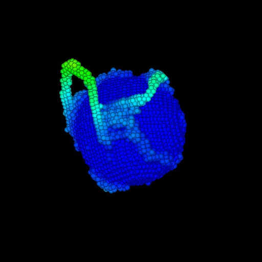
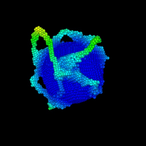
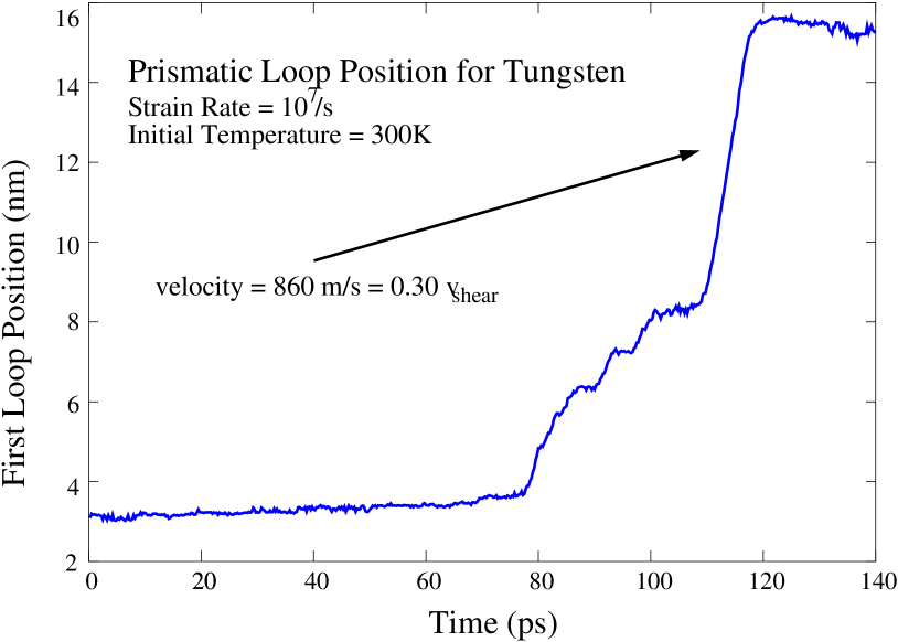
In the bcc metals, the dislocation nucleation process reaches a metastable configuration like that shown in Fig. 6d, and it remains in that configuration for some time before continuing the nucleation process. This quiescent period is apparent in the plot of the position of the loop in Fig. 7a from 100 ps to 105 ps. Here the loop position is taken to be the radial distance of the leading edge of the loop from the centre of the void. By contrast, the position of the loop in the fcc metal [20] shown in Fig. 7b is much smoother in time. In both plots the zero time has been offset by an arbitrary amount. The plateau in the position of the loop in W at 120 ps (Fig. 7a) is due to the loop reaching the boundary of the simulation box where symmetry dictates the driving stress goes to zero so the loop stops moving.

The basic mechanism of this process can be understood by examining its energetics, involving the relaxation of the strain energy as the loop is driven by the stress field of the void. Also important is the line energy of the dislocation and the lattice energy (Peierls barrier) that depends on where the dislocation core is located with respect to the lattice. For our purposes, we will neglect the change in the surface area of the void and the energy associated with elastic image forces. The total energy is then
| (6) |
Each of these terms can be approximated. The Peach-Kohler force per unit dislocation length is given by where is the Burgers vector and is the unit vector in the line direction [56]. The Peach-Kohler force is projected onto the glide direction . We use the void stress field (4), and . The line energy per unit length is given by , where is the shear modulus and is a material-dependent constant of order unity [65]. We multiply this by the loop length, either for a detached loop or for a loop that is still attached to the void surface. The final term is the Peierls energy where is the height of the Peierls barrier [65] and is the length of the leading edge of the dislocation, either (detached) or (attached).
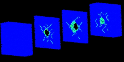
Using approximate parameters for tantalum, the resulting energetics of attached and detached loops are plotted for different tensile stresses in Fig. 8. The plots show that at lower tensile stresses the leading edge of the dislocation is driven by the elastic energy to extend out from the void, as the Peach-Kohler forces overcome the line tension. As the dislocation moves outward, the shear stress drops and the upward turning energy and the lattice barrier stop the dislocation from moving further. As the stress increases, the dislocation moves further out. Eventually, it becomes advantageous to nucleate the rest of the loop so that the detached loop can propagate further from the void, not confined by the line tension. It is interesting to note that the size of the plastic zone in the initially dislocation free crystal is set by the lattice resistance (Peierls barrier) rather than a yield stress due to the dislocation network.
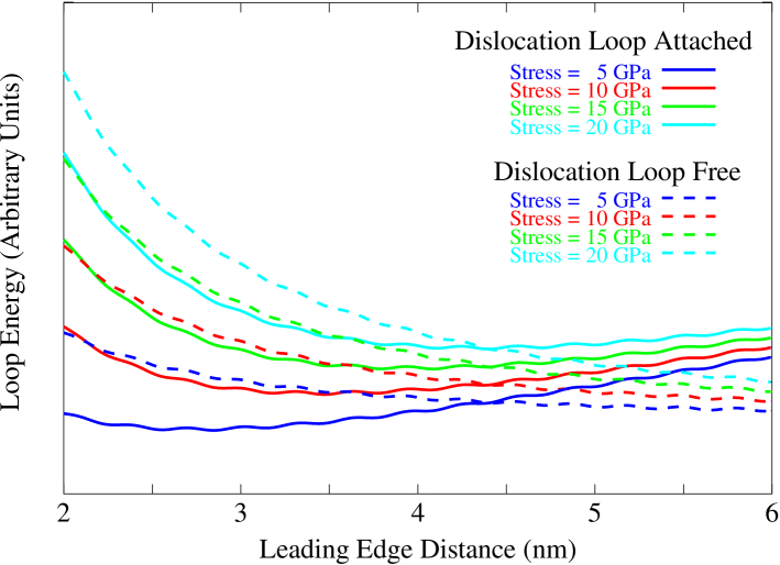
In the fcc metals, the loop nucleation process is much smoother because the Peierls stress is very low compared to the stress needed to nucleate the dislocation from the void surface. Once the loop is punched out, the Peierls barrier provides little resistance to the further glide of the loop. In the bcc metals the Peierls barrier is much higher. It is highest for screw dislocations, but the edge dislocations in the prismatic loops of interest here also have a high Peierls stress, albeit not has high as for screw dislocations [66].
To date there is little experimental evidence for a plastic zone around a void after it has grown, and no means of imaging individual dislocations around a void. One transmission electron micrograph that suggests a plastic zone around a void has been presented by Meyers [57] without quantitative analysis. A differential shading around a void in aluminium sample that was sliced and etched has been suggested to be due to dislocation etch pits in the plastic zone [13]. At this point it is not expected that it will be possible to image dislocations around a void in situ during dynamic fracture any time soon, but improved techniques for quantifying the plastic zone around voids in recovered samples are likely.
5.3 Twinning and Intergranular Fracture
In many metals at high deformation rates or low temperatures, dislocation-mediated plastic deformation cannot support the shear strain rate so the shear stress rises until it reaches a threshold at which twinning occurs [29]. Twins propagate rapidly, leading to a plastic strain rate that equals the rate of change of the twinned volume fraction times the eigenstrain of the twin. A similar phenomenon is observed to occur in these simulations of bcc void growth. If the void growth rate, limited by the rate of nucleation and propagation of dislocations, is too slow, the tensile stress will continue to rise. The stress field around the void changes the tensile stress into a shear stress, and once the shear stress reaches the twinning threshold, twins nucleate and propagate rapidly. If the void grows fast enough, the threshold is never reached.
In practice we observe a threshold in the strain rate such that for sufficiently high strain rates, twins form at the void surface and propagate through the simulation box. The twin boundaries are then observed to fracture leading to a rapid drop in the tensile stress. A visualisation of twin nucleation at the void surface in Ta at a strain rate of /s is shown in Fig. 9.
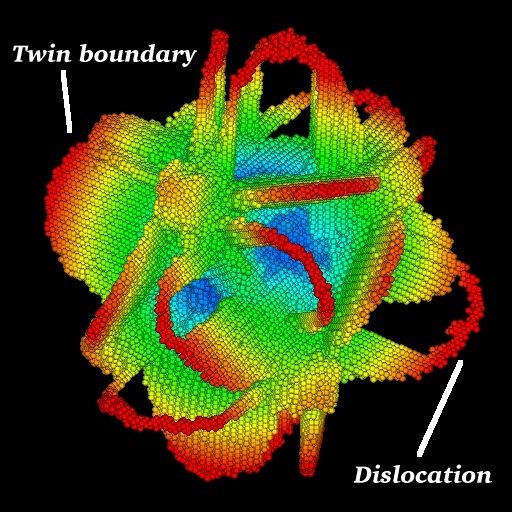
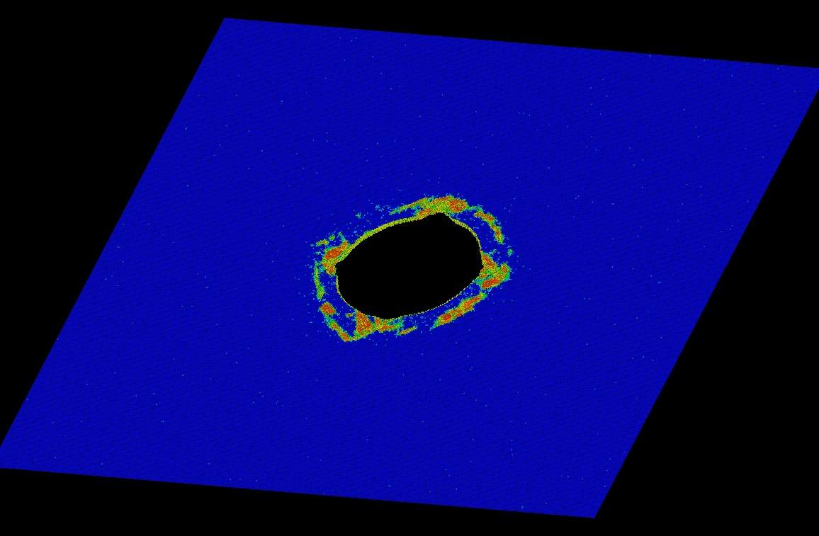
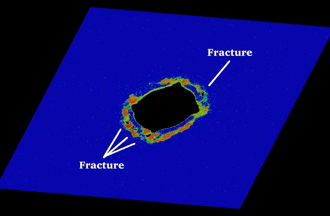
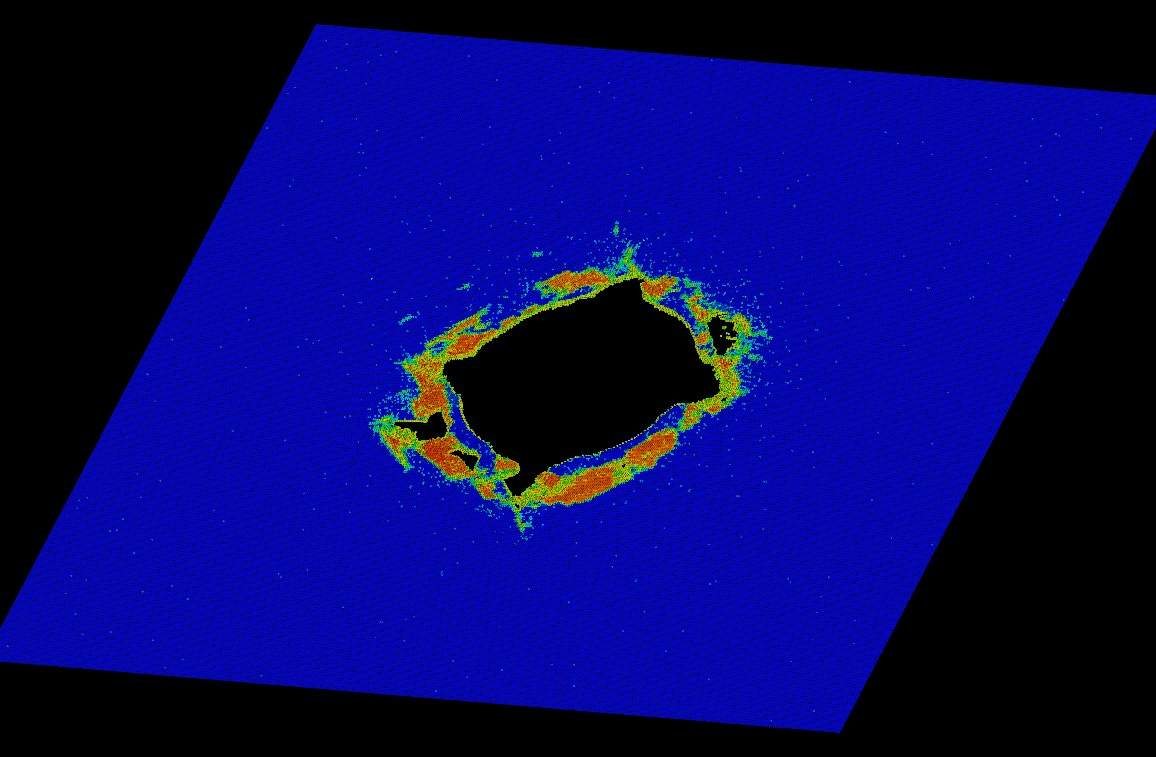
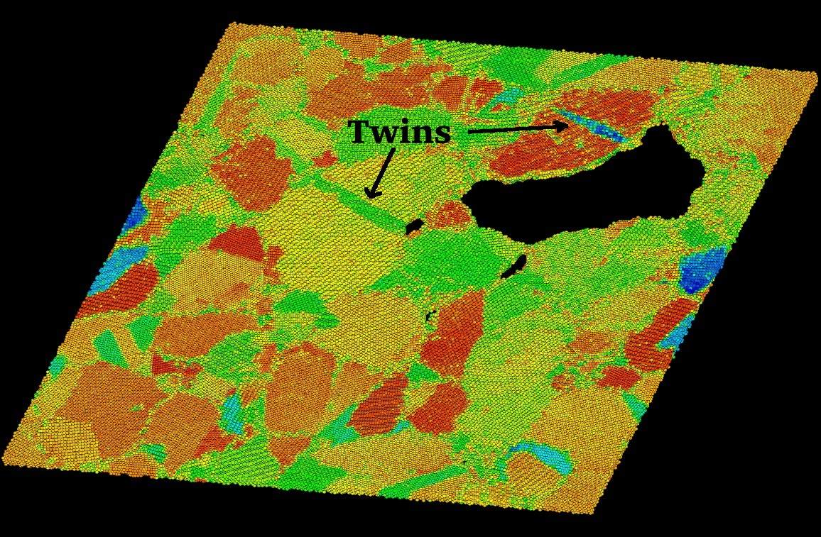
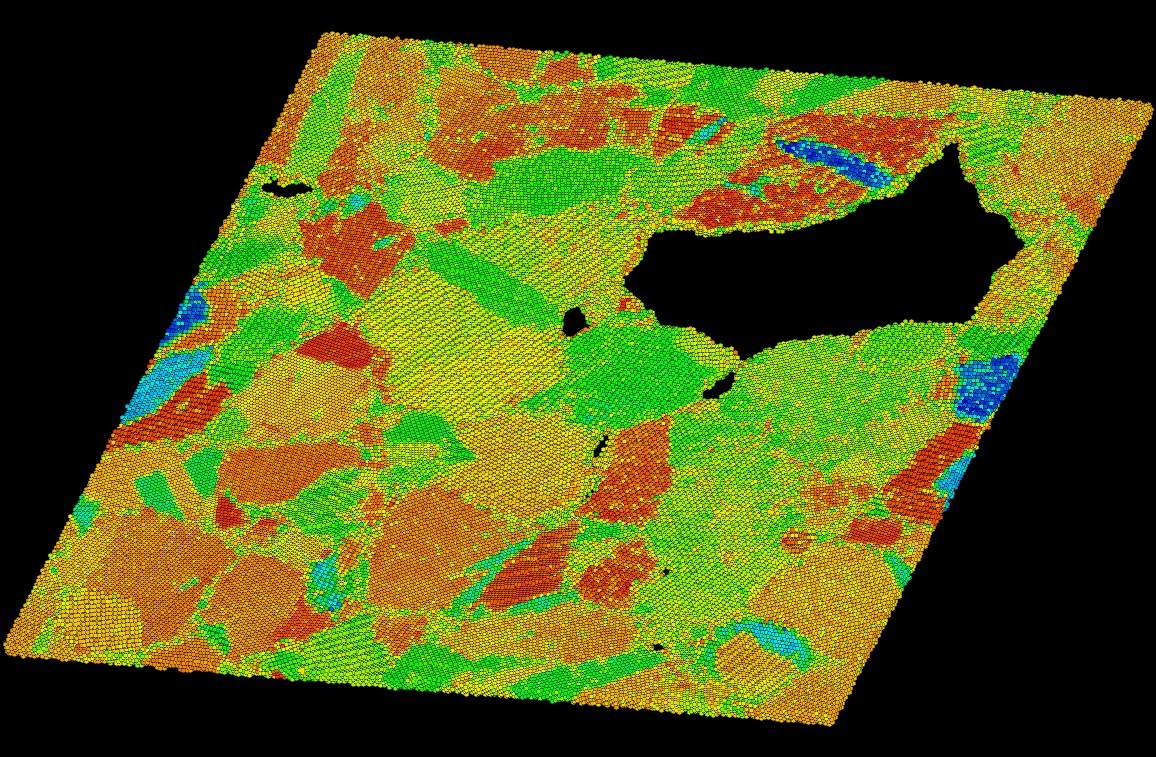
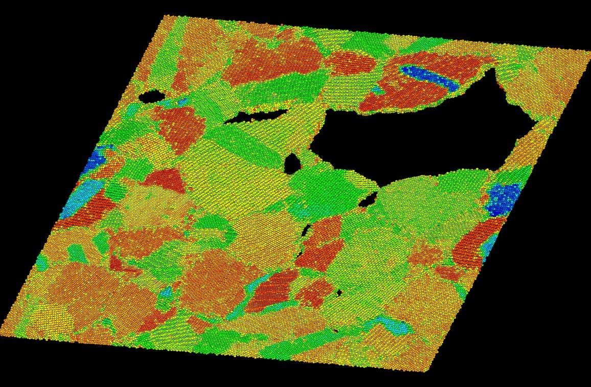
A series of snapshots of a slice through a system as it twins and fractures is shown in Fig. 10, coloured according to the lattice orientation. The change in orientation due to the twins can be seen near the void surface in Fig. 10a. The apparent ring of twinned material around the void is due to twins propagating at an angle from the surface as seen in Fig. 9. In the second panel, Fig. 10b, fracture is beginning to take place along the twin boundaries, and it progresses further in Fig. 10c. The first three panels are spaced equally in time (and strain). The fourth panel is later in time after the system has completely fractured. The time at which the spanning fracture occurs depends on system size, and in a real material fractures like this would link up between voids in a more random fashion rather than immediately spanning the system, but the basic process of twin-mediated fracture is plausible at high rates.
6 Comparison with FCC Voids
The basic mechanism of void growth is the same in bcc and fcc metals, but there are significant differences in some aspects of the process. The Peierls barrier is much lower in fcc metals than in bcc metals, and this difference accounts for many of the differences in the dislocation processes. Also, in fcc metals the stacking fault energy is relatively low so the dislocations are split into partials [65]. These partials limit cross-slip and tend to produce dislocations that are linear over persistence lengths of several nanometres or more. As a result, the prismatic dislocation loops from nanoscale voids form as parallelograms with four straight legs on the {111} glide planes (cf. Fig. 1). The loops in bcc metals, on the other hand, are formed from perfect dislocations rather than partials spanned by stacking fault ribbons, and they have a shorter persistence length, so that loops are more circular even at the nanoscale.
In copper the void surface evolved from an initially spherical shape to a more faceted shape, with low energy {111} facets. The edges connected the facets were rounded, but the void had a definite octahedroid shape, as quantified by the hexadecapole moment [21]. In the bcc metals studied here there is no pronounced faceting of the voids. The {110} surfaces are the close-packed surfaces of the bcc metals, but they do not appear to play a special role on the bcc void surfaces. The voids do not take on the shape of a dodecahedron, although if the edges are rounded, a dodecahedron is very similar to a sphere and it may be that the voids here are too small to see the effect.
In bcc metals the motion of the loops is different, too. The loop nucleation process is fairly smooth in fcc metals, whereas in bcc metals the initial motion of the is jerky as shown in Fig. 7 for tungsten and copper. In both cases the velocities of prismatic loops can be a large fraction of the shear wave velocity. The maximum velocities in the figure are (a) 860 m/s = 30% of the shear wave velocity for tungsten and (b) 1400 m/s = 60% of the shear wave velocity for copper.
7 Nucleation in Polycrystals
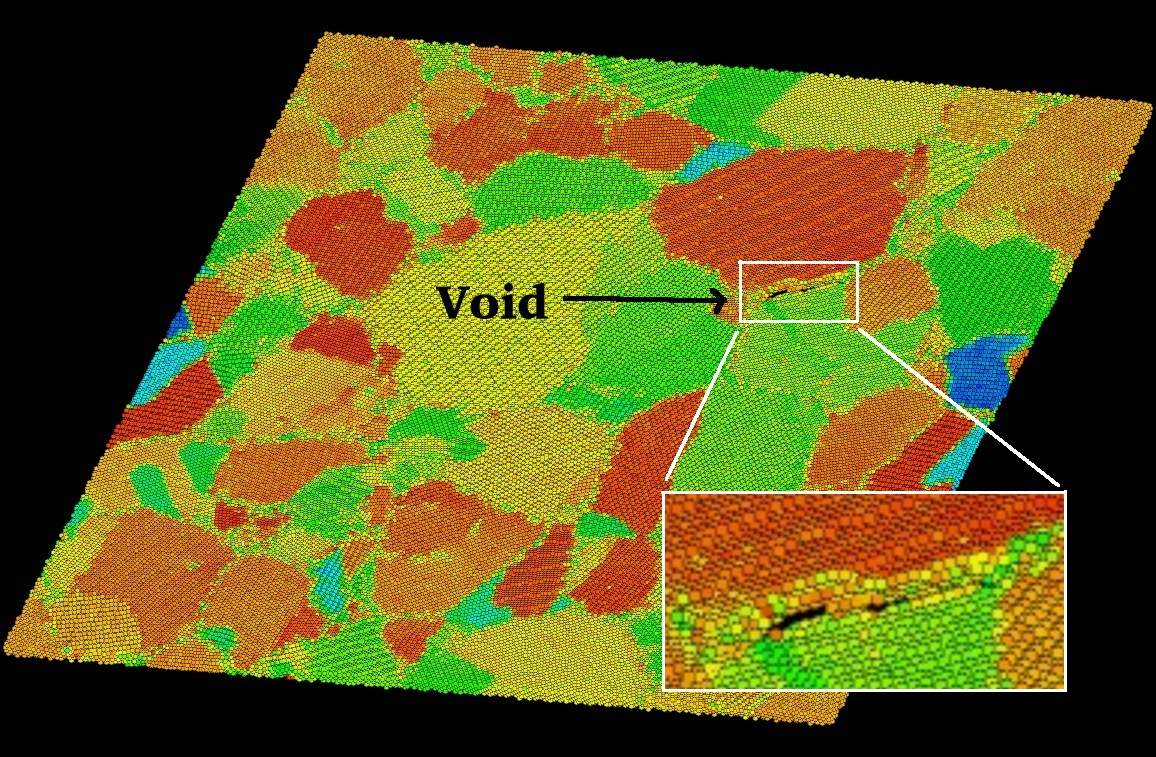
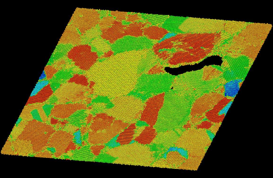
The process of nucleation of voids at grain boundaries in polycrystalline systems is also interesting, both from the point of view of how grain boundaries affect fracture and from the point of view of the extraordinary mechanical properties of nanocrystalline metals [67, 68]. Nanocrystalline tantalum, in particular, has been considered for applications in inertially confined fusion where it would be subjected to high rate loading [27]. We have investigated dynamic fracture in these systems through a series of simulations of void nucleation and growth in an initially fully dense 16-million-atom MD simulation of nanocrystalline Ta. These systems were produced in previous work by Streitz et al. [46] through rapid compression of molten Ta. Previously, we have investigated the plastic flow in this system under uniaxial and biaxial strain at constant volume [48]. Here we investigate how the system responds through the nucleation, growth and coalescence of voids as the volume is increased at a specified strain rate.
Figure 11 shows the stress-strain curve for a nanocrystalline system undergoing dynamic fracture as simulated in molecular dynamics for several different strain rates. As in the single crystal simulations, there is an elastic phase followed by the onset of plasticity and substantial void volume increase leading to a drop in the stress. Also like the single crystal simulations, the peak stress increases as the strain rate increases.

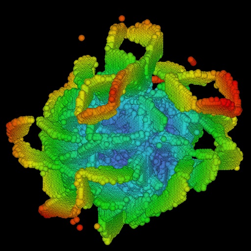
Snapshots from the /s simulation are shown in Fig. 12. The polycrystalline system is coloured according to the quaternion for the local lattice orientation, as described above. Initially, the system is fully dense (Fig. 12a). As the stress increases, voids form at the grain boundary junctions. A sliver of a void is barely visible in the upper right quadrant of Fig. 12b. As the box expands further, the first void open up and additional voids nucleate (Fig. 12c-f). The grains around the large void exhibit dislocation-based plasticity (Fig. 12c) and then twinning (Fig. 12d) in order to accommodate the void growth.
8 Conclusion
Simulation of the nucleation and growth of voids at the atomistic level has provided a wealth of information about the interaction of plasticity with the void. The simulations have shown an elastic phase in which the material stretches followed by a plastic phase in which there is considerable void growth. In the single crystal simulations prismatic dislocation loops are punched out as the void grows. These glissile edge dislocation loops transport a platelet of atoms away from the void, facilitating its growth and reducing the elastic strain energy of the material. The process is similar to the dislocation processes observed in the classic Mitchell experiments in which prismatic loops were punched out due to the strain of a mismatched spherical inclusion [64]. At high strain rates, the simulations showed a propensity to twin and then fracture along the twin boundary.
The nature of the plasticity associated with void growth in the bcc metals is similar to that observed in fcc void growth simulations previously [8]. In both cases prismatic loops have been observed to be punched out and propagate away from the void. At a finer level of detail, the fcc and bcc plastic mechanisms differ substantially. In the bcc dislocation nucleation process the growth occurs in bursts due to the high Peierls barrier and some of the details of the dislocations are different, including a staggered nucleation process and different loop shapes. There is no sign of substantial debris formation as reported for bcc screw dislocations in Ref. [28].
In the nanocrystalline simulations, the fully dense metal was observed to nucleate voids at some of the grain boundary junctions. As these voids grew, the grains surrounding the voids deformed plastically, first through dislocation flow and later through twinning.
In these simulations we have made a number of explicit and implicit assumptions. In the simulations reported here except for the polycrystal, the void is the only defect in the lattice at the start of the simulation. In an engineering metal, a variety of defects is present including grain boundaries, inclusions, and pre-existing dislocations. Here we have focused on the case where those other defects can be neglected, and the adhesion between inclusions and the matrix is sufficiently weak that the inclusion can be modelled as a void. The other defects can be neglected provided their population is sufficiently sparse, as discussed in Section 5. It remains for future work to go to much larger simulations to go to lower loading rates and focus on voids nucleating from larger inclusions surrounded by other defects and microstructural features.
We can elaborate on the condition of only sparse pre-existing dislocations. The dislocation flow required in the plastic zone around a growing void can come from the prismatic content of dislocations emitted from the surface or the prismatic content of dislocations flowing in from the surrounding material. A far-field shear stress does not drive prismatic flow to or from the void; it is the hydrostatic tension with the stress concentration at the void that drives the prismatic flow. So in systems that are driven hard and in which the dislocation density is low so that the mean dislocation spacing is much greater than the size of the voids and void nucleation sites, it is dislocation flow nucleated from the void surface that is important for void growth. This regime has motivated our work.
In the comparison of the peak stress in the MD simulations with the experimental measurement of the Mo spall strength, it was found that the MD under-predicts the stress to initiate spall in bcc metals. In the fcc metal copper studied previously the agreement was much better [8] The disagreement in Mo suggests that if we want to understand the spall strength quantitatively, we either need to simulate the full spallation process, not just single void growth, or we need a potential that has been fit to tensile equation of state (EOS) data and validated, or perhaps both. More sophisticated potentials are available; however, the demands of this application are challenging. The potential not only needs to provide an accurate description of the EOS, elasticity and dislocation mobility in this unusual tensile regime, but it needs to describe the void surface accurately, including surface structure, surface energies and surface stresses. All of these material properties affect the dislocation nucleation process.
The question of plasticity around voids is of interest not only when the voids grow, but also when they collapse. Crush down models have been developed to understand the behaviour of voids and helium bubbles in irradiated materials that are subjected to pressure [69]. Some of the findings here may help shed light on void collapse, as well.
These atomistic simulations have provided a window into the dislocation processes around the void as it nucleates and grows. The single void growth and nanocrystalline void nucleation and growth processes involve complex plastic flow dynamics governed by some fundamental processes including nucleation at weak points such as grain boundary junctions and deformation of the matrix accommodating void growth through a prismatic dislocation flux. There is still much to be learned about void growth during dynamic fracture of bcc metals.
Acknowledgements
It is a pleasure to thank Jim Belak, Eira Seppälä, and Laurent Dupuy for useful discussions, as well as the earlier work on voids in fcc metals. The initial atomic configuration for the nanocrystalline simulations was provided by Streitz, Glosli, and Patel [46]. Computer resources were provided by Livermore Computing through a Supercomputing Grand Challenge project. This work was performed under the auspices of the US Department of Energy by Lawrence Livermore National Laboratory under Contract DE-AC52-07NA27344.
References
- [1] D.R. Curran, L. Seaman, and D.A. Shockey, Phys. Rep. 147 (1987) p.253.
- [2] F.A. McClintock, J. Appl. Mech. 6 (1968) p.363.
- [3] J.R. Rice and D.M. Tracey, J. Mech. Phys. Solids 17 (1969) p.201.
- [4] V. Tvergaard and A. Needleman, Acta Metall. 32 (1984) p.157.
- [5] E. van der Giessen, M. W. D. van der Burg, A. Needleman, and V. Tvergaard, J. Mech. Phys. Solids 43 (1995) p.123.
- [6] X.Y. Wu, K.T. Ramesh, T.W. Wright, J. Mech. Phys. Solids 51 (2003) p.1; Int. J. Solids Structures 40 (2003) p.4461.
- [7] A.L. Stevens, L. Davison and W.E. Warren, J. Appl. Phys. 43 (1972) p.4922.
- [8] R.E. Rudd, E.T. Seppala, L.M. Dupuy, and J. Belak, J. Computer-Aided Mater. Des. 14 (2007) p.425.
- [9] J. Belak, J. Computer-Aided Mater. Des. 5 (1998) p.193.
- [10] R.E. Rudd and J. Belak, Comp. Mater. Science 24 (2002) p.148.
- [11] W.G. Wolfer, Phil. Mag. A 58 (1988) p.285.
- [12] V.A. Lubarda, M.S. Schneider, D.H. Kalantar, B.A. Remington, and M.A. Meyers, Acta Mater. 52 (2004) p.1397.
- [13] D.C. Ahn, P. Sofronis, M. Kumar, J. Belak, and R. Minich, J. Appl. Phys. 101 (2007) p.063514.
- [14] R. Hill, The Mathematical Theory of Plasticity, Clarendon Press, Oxford, 1950.
- [15] A. L. Gurson, J. Eng. Mater. and Tech. 99 (1977) p.2.
- [16] F. A. McClintock in Metall. Eff. at High Strain Rates, (Plenum Press, New York, 1973).
- [17] A.E. Koniges, R.W. Anderson, P. Wang et al., J. de Physique IV 133 (2006) p.587.
- [18] E.M. Bringa, K. Rosolankova, R.E. Rudd et al., Nature Mater. 5 (2006) p.805.
- [19] T.C. Germann, K. Kadau, and P.S. Lomdahl, in Proc. of IEEE/ACM Supercomputing’05 (2005).
- [20] J.A. Moriarty, J.F. Belak, R.E. Rudd, P. Soderlind, F.H. Streitz and L.H. Yang, J. Phys.: Condens. Matter 14 (2002) p.2825.
- [21] E.T. Seppala, J. Belak, and R.E. Rudd, Phys. Rev. B 69 (2004) p.134101.
- [22] E.T. Seppälä, J. Belak, and R.E. Rudd, in Dislocations, Plasticity and Metal Forming, edited by Akhtar S. Khan (NEAT Press, Maryland, 2003).
- [23] L.M. Dupuy and R.E. Rudd, Modelling Simul. Mater. Sci. Eng. 14 (2006) p.229.
- [24] E.T. Seppala, J. Belak, and R.E. Rudd, Phys. Rev. Lett. 93 (2004) p.245503.
- [25] E.T. Seppala, J. Belak, and R.E. Rudd, Phys. Rev. B 71 (2005) p.064112.
- [26] Q. Wei, T. Jiao, K.T. Ramesh, and E. Ma, Scripta Mater. 50 (2004) p.359.
- [27] Y.M. Wang, A.F. Jankowski, and A.V. Hamza, Scripta Mater. 57 (2007) p.301.
- [28] J. Marian, W. Cai, and V.V. Bulatov, Nature Mater. 3 (2004) p.158.
- [29] J.W. Christian and S. Mahajan, Prog. Mater. Sci. 39 (1995) p.1.
- [30] G.T. Gray III and A.D. Rollett, In: High Strain Rate Behavior of Refractory Metals and Alloys, edited by R. Asfahani, E. Chen, and A. Crowson, TMS (1992).
- [31] M. Finnis and J. Sinclair, Phil. Mag. A 50 (1984) p.45.
- [32] A.P. Sutton, M.W. Finnis, D.G. Pettifor, and Y. Ohta, J. Phys. C: Solid State Phys. 21 (1988) p.35.
- [33] D.G. Pettifor, Phys. Rev. Lett. 63 (1989) p.2480.
- [34] M. Mrovec, D. Nguyen-Manh, D.G. Pettifor, and V. Vitek, Phys. Rev. B 69 (2004) p.094115.
- [35] M. Mrovec, R. Gröger, A.G. Bailey, D. Nguyen-Manh, C. Elsässer, and V. Vitek, Phys. Rev. B 75 (2007) p.104119.
- [36] J.A. Moriarty, Phys. Rev. B 42 (1990) p.1609.
- [37] J.A. Moriarty, Phys. Rev. B 49 (1994) p.12431.
- [38] D.R. Mason, R.E. Rudd and A.P. Sutton, Computer Physics Comm. 160 (2004) p.140.
- [39] J.N. Glosli, K.J. Caspersen, D.F. Richards, R.E. Rudd, F.H. Streitz, and J.A. Gunnels, “Micron-scale Simulations of Kelvin-Helmholtz Instability with Atomistic Resolution,” in Proc. Supercomputing 2007 (SC07), Reno, NV, Nov. 2007.
- [40] R.E. Rudd and J.Q. Broughton, Phys. Stat. Sol. 217 (2000) p.251.
- [41] R.E. Rudd and J.Q. Broughton, Phys. Rev. B 72 (2005) p.144104.
- [42] G.J. Ackland and R. Thetford, Phil. Mag. A 56 (1987) p.15.
- [43] J. Marian, J. Knap, and G.H. Campbell, Acta Mater. 56 (2008) p.2389.
- [44] M. Parrinello and A. Rahman, J. Appl. Phys. 52 (1981) 7182.
- [45] M. P. Allen and D. J. Tildesley, Computer Simulations of Liquids, Oxford University Press, Oxford, 1987.
- [46] F.H. Streitz, J.N. Glosli, and M.V. Patel, Phys. Rev. Lett. 96 (2006) p.225701.
- [47] F.H. Streitz, J.N. Glosli, M.V. Patel, B. Chan, R. Yates, B. de Supinski, J. Sexton, and J. Gunnels, in Proc. IEEE/ACM Supercomputing ’05.
- [48] R.E. Rudd, Mater. Sci. Forum, (2009) to appear, arXiv:0902.4491.
- [49] For information on the Livermore Computing supercomputers, see: http://computing.llnl.gov/.
- [50] C. L. Kelchner, S. J. Plimpton, and J. C. Hamilton, Phys. Rev. B 58 (1998) p.11085.
- [51] S.J. Zhou, D.M. Beazley, P.S. Lomdahl, and B.L. Holian, Phys. Rev. Lett. 78 (1997) p.479.
- [52] F.F. Abraham, R. Walkup, H.J. Gao, M. Duchaineau, T. Diaz de la Rubia, and M. Seager, Proc. Natl. Acad. Sci. USA 99 (2002) p.5783.
- [53] H. Goldstein, Classical Mechanics, 2nd ed., Addison-Wesley, Reading, MA, 1980.
- [54] H. Grimmer, Acta Cryst. A30 (1974) p.685.
- [55] D.J. Evans, Mol. Phys. 34 (1977) p.317.
- [56] J.P. Hirth and J. Lothe, Theory of Dislocations, 2nd ed., John Wiley and Sons, New York, 1992.
- [57] M.A. Meyers, Dynamic Behavior of Materials, Wiley-Interscience, New York, 1994.
- [58] J.A. Zimmerman, E.B. Webb, III, J.J. Hoyt, R.E. Jones, P.A. Klein and D.J. Bammann, Modelling Simul. Mater. Sci. Eng. 12 (2004) p.S319.
- [59] A.E.H. Love, The Mathematical Theory of Elasticity, 4th ed., Dover, New York, 1944, §98.
- [60] J.D. Eshelby, Proc. Royal Soc. A 241 (1957) p.376.
- [61] G.I. Kanel et al., J. Appl. Phys. 74 (1993) p.7162.
- [62] H.E. Lorenzana et al., Sci. Model. Simul. 15 (2008) p.159.
- [63] J. Belak, J. Computer-Aided Mater. Des. 9 (2004) p.165.
- [64] J.W. Mitchell, in: R.H. Doremus, B.W. Roberts, D. Turnbull, (eds) Growth and Perfection of Crystals, Wiley, New York, 1958, p.386.
- [65] D. Hull and D.J. Bacon, Introduction to Dislocations, 3rd ed., Pergamon, Oxford, 1984.
- [66] P.B. Hirsch, A. Howie, and M.J. Whelan, Philos. Trans. Roy. Soc. London Series A-Math. Phy. Sci. 252 (1960) p. 499.
- [67] D. Wolf, V. Yamakov, S.R. Phillpot, and A.K. Mukherjee, Z. Metallkd 94 (2003) p.1091.
- [68] H. van Swygenhoven., M. Spaczer, A. Caro, and D. Farkas, Phys. Rev. B 60 (1999) p.22.
- [69] D.B. Reisman, W.G. Wolfer, and A. Elsholz, J. Appl. Phys. 93 (2003) p.8952.