Control and imaging of single-molecule spectral dynamics
using a nano-electrode
Abstract
We study the influence of a scanning nano-electrode on fluorescence excitation spectra of single terrylene molecules embedded in thin p-terphenyl films at cryogenic temperatures. We show that applied voltages less than 10 V can result in reversible Stark shifts of up to 100 times and linewidth increase greater than 10 times the natural linewidth. We discuss the potential of our experimental scheme for direct imaging of individual two-level systems (TLS) in the nanometer vicinity of single molecules.
Spectral dynamics (SD) is caused by the interaction of an emitter with its surrounding matrix and is known to take place both in crystalline and amorphous matrices. Depending on the time scale of measurement, SD appears as discrete frequency jumps or broadening of resonances. The nanoscopic origin of the emitter-matrix interaction can vary in different cases and is in general poorly understood. Nevertheless, the effects of the matrix can be formulated in a phenomenological manner by considering the potential energy surface that results from the large number of possible interactions between the emitter and the constituents of the matrix. This energy landscape can be treated as a reservoir of double-well potentials Heuer and Silbey (1993) with their lowest energy levels referred to as two-level systems (TLS) Phillips (1972); Anderson et al. (1972); Geva and Skinner (1997). Tunneling between the potential wells gives rise to SD which can be mediated via mechanical, magnetic, electric, or acoustic interactions. In what follows, we restrict ourselves to the influence of external electric fields on the SD of zero-phonon lines (ZPL) of organic dye molecules at cryogenic temperatures.
Although in an amorphous matrix the emitter is expected to interact with a sea of TLSs, it is possible that one or only few TLSs dominate in a crystalline environment, leading to discrete jumps. One such an example was discovered for terrylene molecules embedded in p-terphenyl (pT), in which guest molecules in certain sites undergo well-defined spectral jumps under laser illumination Kulzer et al. (1997); Bordat and Brown (2002). Another case of light-induced reversible spectral jumps was demonstrated for terrylene in naphthalene Bach et al. (1999) by exciting triplet states of the matrix molecules. Nanomechanical interactions have also been shown to cause SD in a reversible fashion in recent near-field spectroscopy experiments Gerhardt et al. (2007). An elegant avenue for external control of TLSs, which is of central concern in this article, is via application of electric fields Maier et al. (1995). Segura et al. observed the narrowing of the ZPLs in two individual pentacene molecules embedded in pT when they applied a voltage to a micro-electrode put in contact with the sample Segura et al. (2001). A related experiment was performed on terrylene in n-hexadecane by Bauer et al. Bauer and Kador (2003), who found many cases of double resonances, which could be split further and experienced changes in their peak intensities under electric fields. Both of the above-mentioned experiments estimated large dipole moments up to 8 Debye for a TLS.
Exploration and control of the interaction between single emitters and their nanoscopic environments provide very valuable insight into various optical phenomena in the condensed phase, and they might open doors for engineering new quantum systems. In this article, we present experiments that employ metal-coated glass fiber tips as scanning nano-electrodes to apply local electric fields on thin pT samples doped with terrylene molecules. We report large modifications of the ZPL linewidths and discuss future directions for imaging single TLSs and their interaction with neighboring single molecules.
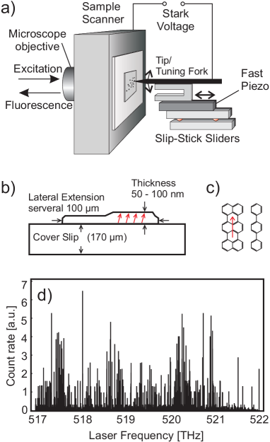
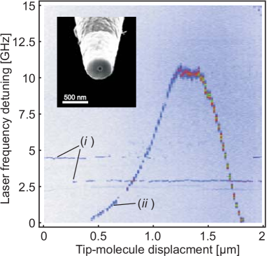
In order to achieve a high spatial resolution in manipulating the TLS, one requires large electric field gradients, ideally changing the observed spectrum of the emitter by more than one linewidth over a length scale of about one nanometer. As displayed in Fig. 1a, the machinery of scanning near-field optical microscopy (SNOM) provides a convenient way for realizing this scheme. To produce a well-defined SNOM probe, we pulled glass fiber tip and coated them with aluminum and milled at the end by a focused ion beam Veerman et al. (1998). An electron micrograph of such a probe is shown as an inset in Fig. 2. Home-built slip-stick sliders allowed us to position the tip at a desired location with sub-micrometer accuracy. The probe-sample distance was controlled via the shear-force interaction using commercially available quartz tuning forks with a resonance frequency of 32 kHz Karrai and Grober (1995). In this scheme, lateral (sub-)nanometer oscillations of the tip are measured by a lock-in amplifier that monitors the current created in the tuning fork. At very small separations of a few tens of nanometers from the sample, the tip oscillation is damped owing to the so-called shear-force effect. This provides an error signal that is used to control the tip position and to prevent if from crashing into the sample. A piezo-electric scanner was used to scan the sample more than six micrometers with nanometer accuracy in all directions. Further details of our cryogenic confocal-SNOM setup can be found in Refs. Hettich et al. (2002); Gerhardt et al. (2007).
In our current work, we used the SNOM tip only as a nano-electrode for applying a local electric field, while the cryostat body was grounded and used as the counter-electrode (see Fig. 1a). Furthermore, we adjusted the tip-sample separation at about 100 nm to rule out any mechanical contact Gerhardt et al. (2007) or near-field effects related to the van der Waals interaction Chance et al. (1978); Bian et al. (1995). Optical measurements were not performed through the tip, as is usually done in SNOM; instead, we used a microscope objective on the other side of the sample to both excite the molecules and collect their fluorescence in the far field. To record fluorescence excitation spectra of a single terrylene molecule, we used a narrow-band dye laser (Coherent Autoscan, 899-21, 577 nm) to excite it selectively and detected its Stokes-shifted fluorescence on an avalanche photodiode through an optical long-pass filter (Omega-Optical, Kaiser notch-filter) Orrit and Bernard (1990).
Electric fields at the end of a sharp electrode drop rapidly at distances larger than the tip diameter Jackson (1999); Hettich et al. (2002). Therefore, to ensure a strong spatial gradient, it is important to place the molecule of interest as close to the tip as possible. We, thus, performed our experiments on thin pT films Sandoghdar et al. (2001); Pfab et al. (2004). Briefly, a piraña-cleaned cover slip was spin coated with a solution of pT in toluene (3 mg/ml) doped with terrylene molecules at a concentration of about . This resulted in typical film thickness of about 20-30 nm. However, cryogenic fluorescence excitation spectra revealed spectral jumps and typical linewidths of several hundered MHz, which are many times larger than the natural linewidth of 40 MHz for terrylene in pT. To minimize the residual SD, we annealed the samples at 60°C for 60 min in air. As a result, pT films were split to islands with thicknesses increased to 50-100 nm (see Fig. 1b). Contrary to what is known from bulk samples Kummer et al. (1997), Fig. 1d shows that the inhomogeneous distribution of the ZPLs did not show well-defined spectral sites in these islands. We mention in passing that we observed a bunching of molecules near crystal island edges in wide-field images. To avoid possible complications related to edges, we performed our measurements on molecules several micrometers from the rims. Furthermore, we occasionally witnessed spontaneous cracks in the films even days after introduction of the sample into the cryostat, pointing to internal strain in parts of the sample. Nevertheless, the annealing procedure allowed us to re-gain lifetime-limited linewidths of 40-50 MHz in some single molecule spectra.
Figure 2 displays spectra recorded from two molecules as a grounded tip was scanned laterally along a line and at a constant height of 100 nm. Molecule (i) is not directly affected by the tip because it is not close enough to it. However, we clearly see discrete and reversibly recurring spectral jumps between two well-defined frequencies (at about 2.7 and 4.5 GHz on the vertical axis). In case of molecule (ii), the ZPL is shifted by more than 10 GHz as the tip crosses the molecule. A plateau of 300 nm clearly mirrors the tip shape. We also notice that the largest frequency shift is accompanied by the broadening of the resonance. It turns out that although the SNOM tip was grounded, the large frequency shift encountered in Fig. 2 can be explained by a Stark shift.
The Stark shift produced by an external electric field can be expressed as
| (1) | |||||
where is the difference between the electric dipole moments of the excited and ground states, is the difference in the polarizabilities of the two states, and represents a residual electric field in the system Basché et al. (1996). For a single terrylene molecule in a centro-symmetric environment with no disorder , so that only shows a quadratic dependence. In a host system with broken symmetry, however, the linear effect can dominate. Furthermore, if there are any residual electric fields in the sample, for example due to external charges, the second term of Eq. (1) can give rise to a contribution that is linear in .
In Fig. 3a, we varied the applied voltage to a stationary nano-electrode placed above the molecule and recorded fluorescence excitation spectra. Each frequency scan took 14.4 s at a resolution of 25 MHz and integration time of 30 ms per frequency pixel. We find a linear blue Stark shift for increasing positive voltages. However, as reported in Ref. Bauer and Kador (2004a), we have also observed the opposite effect for different molecules under the same tip. A similar spectral behavior has been observed for the XY-site of terrylene in pT Kulzer et al. (1999), but as mentioned earlier, our samples do not show any evidence of well-defined sites (see Fig. 1d). A rough estimate yields effective field strengths up to 1 MV/cm applied to the molecule, which is about two orders of magnitude stronger than in earlier single molecule experiments Segura et al. (2001); Bauer and Kador (2003, 2004a, 2004b).
Interestingly, the observed linear Stark effect in Fig. 3a is accompanied by a change in the spectral line shape, while the area below the resonance remains constant to within approximately 20% over the whole voltage range of -15 to +15 V. Figure 3b depicts a few examples for a closer scrutiny. We find that the resonance line becomes a narrow Lorentzian shape with a full width at half-maximum of 130 MHz at an applied voltage of about 5 V. The data in Figs. 3a and 2 reveal that for this molecule, the unperturbed ZPL of 66 MHz is broadened if a grounded tip is placed above it. It is possible that our nano-electrodes are charged in the fabrication process, which involves focused-ion-beam milling and electron microscopy. An oxide layer formed on the aluminium-coated tip during handling in air might embed these charges and protect them even when the tip shaft is grounded. A nonzero residual electric field might also exist in the pT sample. In any event, Fig. 3 shows that application of 5 V minimizes the effect of . At the same time, both positive and negative fields of larger magnitudes broaden the line to well beyond its value at .
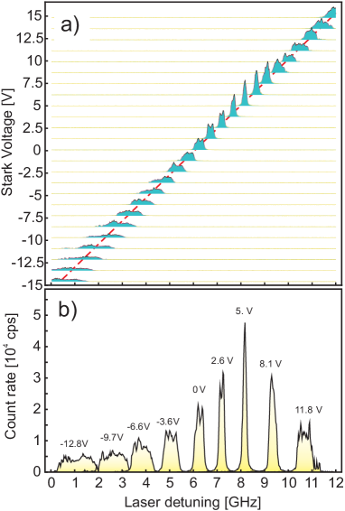
Clearly, a simple Stark effect is not expected to affect the resonance line shape. We also ruled out any systematic effect of tip oscillation and possible modulation of Stark shift by verifying that the spectra in Fig. 3 did not change when we switched off the 32 kHz dither of the tuning fork. On the other hand, the strong response of the spectra to the applied voltages let us attribute the observed broadenings to the electric field-induced SD as reported in Refs. Maier et al. (1995); Segura et al. (2001); Bauer and Kador (2003). In this frame, electric polarization of a TLS in the vicinity of the molecule modifies the relative depths of its two potential wells. The new energy landscape determines whether the tunneling process is accelerated or slowed down in the presence of the tip. Broadenings greater than 1.5 GHz at large applied voltages indicate the activation of many TLSs and fast tunneling rates, contrary to the cases encountered by Bauer et al. Bauer and Kador (2003), where single TLSs could be identified.
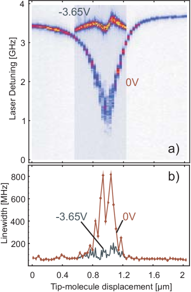
Having discussed the mechanism of electric field-induced broadenings, we turn our attention to Fig. 4a, where spectra recorded on a different single molecule and with another tip are presented. This time, we observed broadenings as large as 800 MHz accompanying a shift of 1.8 GHz over a lateral tip displacement of about 150 nm. However, as the upper curve of Fig. 4a plots, both the shift and broadening of the spectra were strongly reduced when a voltage of -3.65 V was applied to the tip. In particular, we see that the originally unperturbed linewidth of 50 MHz can be recovered, demonstrating a reversible on-command manipulation of the TLS-molecule interaction. The dip in the upper curve of Fig. 4a is most likely caused by the opening in the metal coating of the SNOM tip (see inset in Fig. 1). As mentioned earlier, near-field surface effects related to the van der Waals interaction Chance et al. (1978); Bian et al. (1995) are not expected to play a significant role in our experiments because of a relatively large molecule-tip separations of about 100 nm.
In a previous study, we have shown that the position-dependent Stark shift produced by a scanning micro-electrode can be used to localize single molecules with nanometer accuracy Hettich et al. (2002). We now propose that the position-dependent broadening observed in Figs. 2 and 4 can be exploited to localize a TLS. The centers of the linewidth profiles in these figures cannot be determined with good accuracy because of a relatively large tip plateau and its aperture (see inset in Fig. 2). However, the large field gradient created by the edge of the SNOM tip gives rise to the sharp slope of 22 MHz/nm, or equivalently, one natural linewidth per 2-3 nm. Use of sharper tips and higher electric field gradients should provide substantially higher position sensitivity, allowing one to resolve individual TLSs in the vicinity of a molecule.
In conclusion, we have demonstrated in-situ manipulation and control of the phononic interaction of a single molecule with its nano-environment. We have applied a scanning nano-electrode to show that local application of static electric fields as small as 0-10 V can not only induce large Stark shifts of several GHz in the optical transition of an emitter, but also change its spectral linewidth. Extension of our experimental scheme to sharper electrodes than those used in this work will make it possible to image both a single molecule and the TLSs in its immediate neighborhood simultaneously, and thus, identify the origins of spectral dynamics at the molecular level.
We thank Joy Tharian and Phillipe Gasser at the Swiss Federal Institute for Material Research (EMPA) for their help in producing optical near-field tips and Robert Pfab and Enrico Klotzsch for their contributions to the early stage of sample preparation. This work was financed by the Schweizerische Nationalfond (SNF).
References
- Heuer and Silbey (1993) A. Heuer and R. J. Silbey, Phys. Rev. Lett. 70, 3911 (1993), URL http://link.aps.org/doi/10.1103/PhysRevLett.70.3911.
- Phillips (1972) W. A. Phillips, J. Low Temp. Phys. 7, 351 (1972), URL http://dx.doi.org/10.1007/BF00660072.
- Anderson et al. (1972) P. W. Anderson, B. I. Halperin, and C. M. Varma, Phil. Mag. 25, 1 (1972), URL http://www.informaworld.com/10.1080/14786437208229210.
- Geva and Skinner (1997) E. Geva and J. L. Skinner, J. Phys. Chem. B 101, 8920 (1997), URL http://dx.doi.org/10.1021/jp971722o.
- Kulzer et al. (1997) F. Kulzer, S. Kummer, R. Matzke, C. Bräuchle, and T. Basché, Nature 387, 688 (1997), ISSN 0028-0836, URL http://www.nature.com/nature/journal/v387/n6634/abs/387688a0.%html.
- Bordat and Brown (2002) P. Bordat and R. Brown, J. Chem. Phys. 116, 229 (2002), URL http://link.aip.org/link/?JCPSA6/116/229/1.
- Bach et al. (1999) H. Bach, A. Renn, G. Zumofen, and U. P. Wild, Phys. Rev. Lett. 82, 2195 (1999), URL http://link.aps.org/doi/10.1103/PhysRevLett.82.2195.
- Gerhardt et al. (2007) I. Gerhardt, G. Wrigge, M. Agio, P. Bushev, G. Zumofen, and V. Sandoghdar, Opt. Lett. 32, 1420 (2007), URL http://www.opticsinfobase.org/ol/abstract.cfm?URI=ol-32-11-14%20.
- Maier et al. (1995) H. Maier, R. Wunderlich, D. Haarer, B. M. Kharlamov, and S. G. Kulikov, Phys. Rev. Lett. 74, 5252 (1995), URL http://link.aps.org/doi/10.1103/PhysRevLett.74.5252.
- Segura et al. (2001) J. M. Segura, G. Zumofen, A. Renn, B. Hecht, and U. P. Wild, Chemical Physics Letters 340, 77 (2001), URL http://dx.doi.org/10.1016/S0009-2614(01)00384-0.
- Bauer and Kador (2003) M. Bauer and L. Kador, J. Chem. Phys. 118, 9069 (2003), URL http://link.aip.org/link/?JCPSA6/118/9069/1.
- Veerman et al. (1998) J. A. Veerman, A. M. Otter, L. Kuipers, and N. F. van Hulst, Applied Physics Letters 72, 3115 (1998), URL http://dx.doi.org/10.1063/1.121564.
- Karrai and Grober (1995) K. Karrai and R. D. Grober, Applied Physics Letters 66, 1842 (1995), URL http://dx.doi.org/10.1063/1.113340.
- Hettich et al. (2002) C. Hettich, C. Schmitt, J. Zitzmann, S. Kühn, I. Gerhardt, and V. Sandoghdar, Science 298, 385 (2002), URL http://dx.doi.org/10.1126/science.1075606.
- Chance et al. (1978) R. R. Chance, A. Prock, and R. Silbey, Adv. Chem. Phys. 37, 1 (1978), URL http://dx.doi.org/10.1002/9780470142561.ch1.
- Bian et al. (1995) R. X. Bian, R. C. Dunn, X. S. Xie, and P. T. Leung, Phys. Rev. Lett. 75, 4772 (1995), URL http://link.aps.org/doi/10.1103/PhysRevLett.75.4772.
- Orrit and Bernard (1990) Orrit and Bernard, Phys Rev Lett 65, 2716 (1990), URL http://link.aps.org/doi/10.1103/PhysRevLett.65.2716.
- Jackson (1999) D. Jackson, Classical Electrodynamics (Wiley and Sons, 1999).
- Sandoghdar et al. (2001) V. Sandoghdar, J. Michaelis, C. Hettich, C. Schmitt, J. Zitzmann, and S. Kühn, Single Molecules 2, 277 (2001), URL http://dx.doi.org/10.1002/1438-5171(200112)2:4<277::AID-SIMO2%%****␣gerhardt.tex␣Line␣575␣****77>3.0.CO;2-Y.
- Pfab et al. (2004) R. J. Pfab, J. Zimmermann, C. Hettich, I. Gerhardt, A. Renn, and V. Sandoghdar, Chemical Physics Letters 387, 490 (2004), URL http://dx.doi.org/10.1016/j.cplett.2004.02.040.
- Kummer et al. (1997) S. Kummer, F. Kulzer, R. Kettner, T. Basché, C. Tietz, C. Glowatz, and C. Kryschi, J. Chem. Phys. 107, 7673 (1997), URL http://link.aip.org/link/?JCPSA6/107/7673/1.
- Basché et al. (1996) T. Basché, S. Kummer, and C. Bräuchle, in ”Single-Molecule Optical Detection, Imaging and Spectroscopy”, Edited by T. Basché, W. E. Moerner, M. Orrit, and U. P. Wild, VCH Verlagsgesellschaft GmbH, D-Weinheim (1996), URL http://dx.doi.org/10.1002/9783527614714.
- Bauer and Kador (2004a) M. Bauer and L. Kador, J. Chem. Phys. 120, 10278 (2004a), URL http://dx.doi.org/10.1063/1.1737305.
- Kulzer et al. (1999) F. Kulzer, R. Matzke, C. Bräeuchle, and T. Basché, J. Phys. Chem. A 103, 2408 (1999), URL http://dx.doi.org/10.1021/jp9839448.
- Bauer and Kador (2004b) M. Bauer and L. Kador, J. Lum. 107, 32 (2004b), URL http://dx.doi.org/10.1016/j.jlumin.2003.12.033.