The Kondo Effect in Ferromagnetic Atomic Contacts
Abstract
Iron, cobalt and nickel are archetypal ferromagnetic metals. In bulk, electronic conduction in these materials takes place mainly through the and electrons, whereas the magnetic moments are mostly in the narrow -electron bands, where they tend to align. This general picture may change at the nanoscale because electrons at the surfaces of materials experience interactions that differ from those in the bulk. Here we show direct evidence for such changes: electronic transport in atomic-scale contacts of pure ferromagnets (iron, cobalt and nickel), despite their strong bulk ferromagnetism, unexpectedly reveal Kondo physics, that is, the screening of local magnetic moments by the conduction electrons below a characteristic temperature Kondo (1964). The Kondo effect creates a sharp resonance at the Fermi energy, affecting the electrical properties of the system;this appears as a Fano-Kondo resonance Fano (1961) in the conductance characteristics as observed in other artificial nanostructuresGoldhaber-Gordon et al. (1998); Cronenwett et al. (1998); Park et al. (2002); Liang et al. (2002); Nygard et al. (2000); Yu and Natelson (2003); Mandhavan et al. (1998); Li et al. (1998); Néel et al. (2007). The study of hundreds of contacts shows material-dependent lognormal distributions of the resonance width that arise naturally from Kondo theory Hewson (1993). These resonances broaden and disappear with increasing temperature, also as in standard Kondo systems Cronenwett et al. (1998); Park et al. (2002); Liang et al. (2002); Nygard et al. (2000). Our observations, supported by calculations, imply that coordination changes can significantly modify magnetism at the nanoscale. Therefore, in addition to standard micromagnetic physics, strong electronic correlations along with atomic-scale geometry need to be considered when investigating the magnetic properties of magnetic nanostructures.
Atomic-scale contacts can be fabricated by techniques such as scanning tunnelling microscopy Agraït et al. (2003) or the use of electromigrated break junctions (EBJs)Park et al. (1999), where the size of a macroscopic contact between two leads is reduced until they are in contact through only a few atoms and, eventually, through only one. The conductance of metallic monatomic contacts is known to be around , where is the spin-resolved quantum of conductanceAgraït et al. (2003) ( being the elementary charge and Planck′s constant). To identify the atomic contacts, histograms are constructed from the evolution of the conductance recorded during the breaking of different contacts (Fig. 1a, b). The position of the first peak of these histograms is identified as the conductance of the monatomic contact. For iron, cobalt and nickel, the conductance is larger than owing to the contribution of the and orbitals to the transmission Untiedt et al. (2004); Jacob et al. (2005); Calvo et al. (2008).
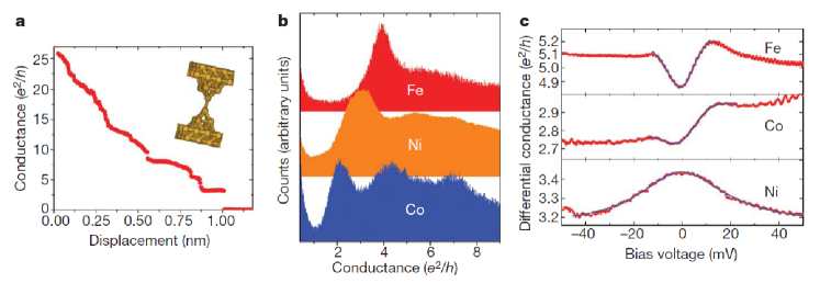
We have studied the low-temperature conductance characteristics of hundreds of atomic-scale contacts of the three transition-metal ferromagnets iron, cobalt and nickel using a home-built STM. More than the 80% of the differential conductance (d/d) curves at the monatomic contact show peaks or dips around zero bias such as those shown in Fig. 1c, which are very similar to those observed in STM spectroscopy of single magnetic adatoms on non-magnetic surfacesMandhavan et al. (1998); Li et al. (1998); Néel et al. (2007). Thus, as in the case of these Kondo systems, we can also fit our d/d curves to the sum of a flat component, , and a Fano-like resonance that typically amounts for 10% of the signal:
| (1) |
Here is the bias shifted with respect to the centre of the resonance, , and normalized by the natural width of the resonance, ; is the Kondo temperature; is the dimensionless Fano parameter that determines de simmetry of the curve; is the amplitude of the feature; and is Boltzmann’s constant.
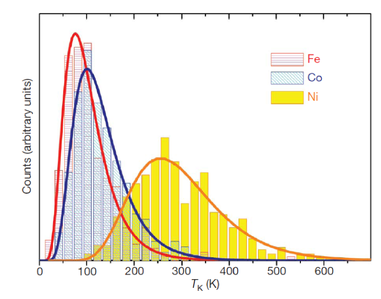
It is clear from the d/d characteristics in Fig. 1c that the width of the Fano feature is different for each material. This is confirmed by statistical analysis of the data. Figure 2 shows histograms of obtained from fitting our conductance curves for hundreds of different iron, cobalt and nickel monatomic contacts. Notably, these histograms follow a log-normal distribution; that is, the natural logarithm of is normally distributed. Because many different atomic configurations result in monatomic contacts, their electronic properties, such as conductance (Fig. 1b), density of states and the associated energy scales, are expected to be normally distributed. Instead, a normal distribution of can only be understood if can be expressed as the exponential of normally distributed quantities. The Kondo modelHewson (1993) naturally relates to the exponential of the typical energy scales in the problem.
Fitting the histograms to a log-normal distribution yields most frequent values for the resonance widths in the different materials corresponding to =90 K, 120 K and 280 K for iron, cobalt and nickel, respectively, following the same trend () for these chemical species when deposited as adatoms on non-magnetic surfacesJamneala et al. (2000). In simple terms, the Kondo temperature decreases as the size of the screened magnetic moment increases, as we change from nickel to cobalt to iron. The Kondo temperature of cobalt nanocontacts is very similar to the one reported in ref. Néel et al. (2007) for cobalt in Cu(100) probed using a STM in the contact regime.
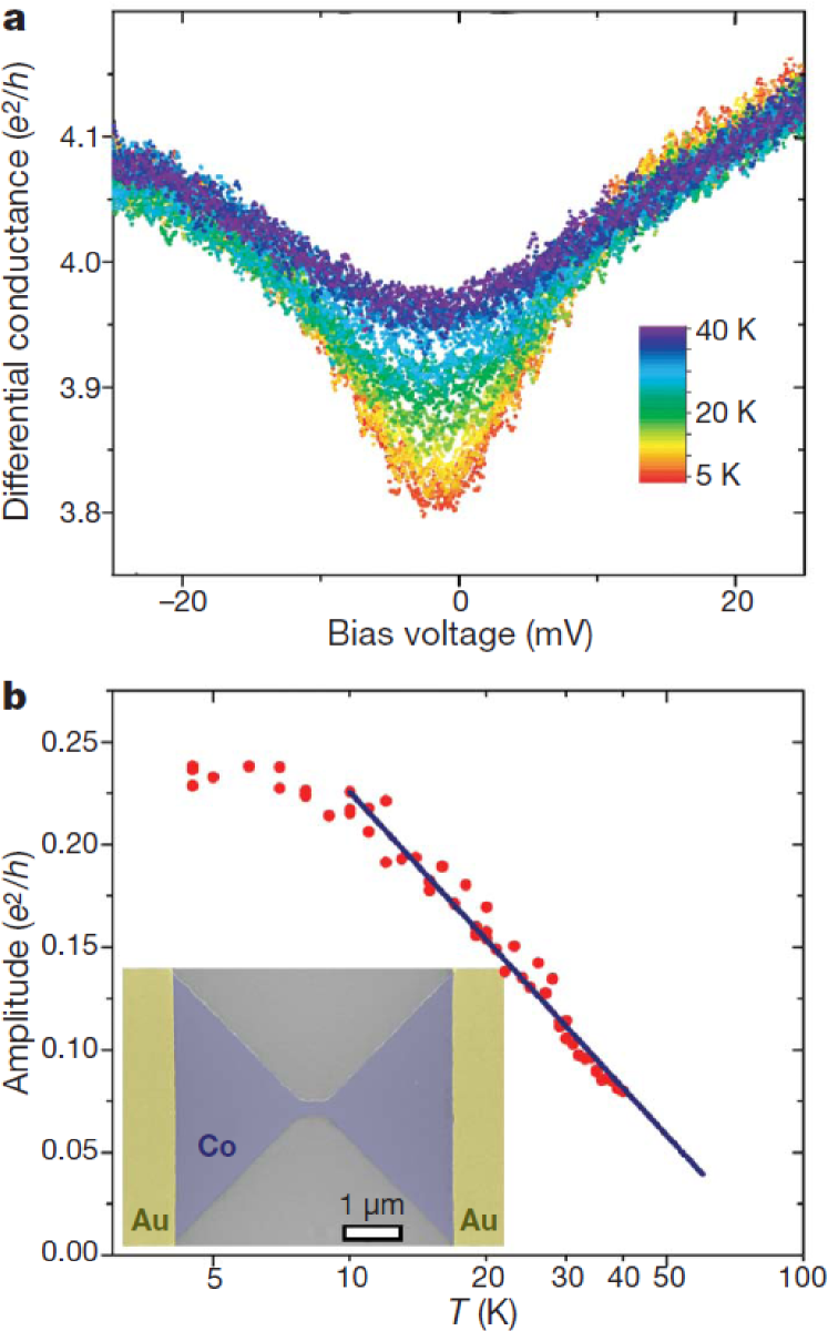
In addition to the statistical analysis described above, we measured the temperature evolution of the Kondo features for a single contact. To preserve the atomic stability of the junction while changing the temperature Keane et al. (2006), we used an EBJ such as the one shown in the inset of Fig. 3b. It is important to note that in this alternative implementation we observe exactly the same Fano resonances, with the same distribution of Kondo temperatures, as we obtained in the STM experiments using nickel and cobalt samples. In all the cases, we see a reduction of the amplitude of the Fano features as the temperature increases, as shown in Fig. 3a for the case of cobalt. In Fig. 3b we plot , as defined in equation (1), as a function of on a logarithmic scale. The curve so obtained has a low-temperature plateau followed by a linear decay, very similar to that of quantum dots and molecules in the Kondo regime Cronenwett et al. (1998); Park et al. (2002); Liang et al. (2002); van der Wiel et al. (2000).
In summary, our atomic contacts fabricated with two different methods show the same d/d curves (Fig. 1c), the same chemical trends (Fig. 2) and the same temperature evolution (Fig. 3a, b) as other standard, chemically inhomogeneous Kondo systems. This indicates that the contact atom(s) in nanocontacts of iron, cobalt and nickel are in the Kondo regime. This is unexpected for two reasons. First, the Kondo effect has always been associated with chemically inhomogeneous systems containing at least two kinds of atom: those where the localized level resides and those providing the itinerant electrons. Here the same chemical species hosts both the itinerant states and the local magnetic moments. Second, in most reports on the Kondo effect, the itinerant electrons are not spin-polarized, as a large spin polarization is expected to destroy the effect. or a carbon nanotube Hauptmann et al. (2008) contacted with ferromagnetic leads has been justified by the oppositely directed spin polarizations in the electrodes, in agreement with refs. Martinek et al. (2003); Martinek (2003); Choi et al. (2004). Although the situation regarding the magnetization of the leads might be similar in our system, we argue that the Kondo effect is still possible even if there is no domain wall pinned in the contact.
Being in the Kondo regime implies that the atoms at the contact must host, at least, a localized -electron level whose magnetic moment is screened as a result of antiferromagnetic coupling to the conduction electrons. We can show how local moment formation and antiferromagnetic coupling occur in nickel nanocontacts in the following way (the cases of iron and cobalt can be understood on similar grounds). The mean-field solution of the Anderson model Anderson (1961),which describes a localized level, with energy , on-site repulsion and hybridization with the itinerant electrons, , defines the conditions for the formation of a local moment in such a level. The model can also be used to derive the antiferromagnetic exchange coupling, (ref. Schrieffer and Wolff (1966)), which arises from the hybridization term. Here we used the local spin-density approximation (LSDA) to density functional theory and its generalization LSDA+U as the mean field to determine the formation of a local moment and its antiferromagnetic coupling to the carriers. We consider both monostrand chains and nanocontacts. Their smaller atomic coordination, compared with that of the bulk, results in a stronger electronic localization and a larger magnetic moment per atom (values of 1.17 Bohr magnetons, compared with 0.6 Bohr magnetons in the bulk, were obtained using LSDA). This favours the appearance of the Kondo effect. In Fig. 4a, b, we show the LSDA bands obtained for the nickel chain. Out of the six minority-spin bands crossing the Fermi level, the two degenerate E2 bands are the narrowest, hosting highly localized electrons. These are the bands that are less well described by the LSDA because of the inherent self-interaction problem of this approximation.
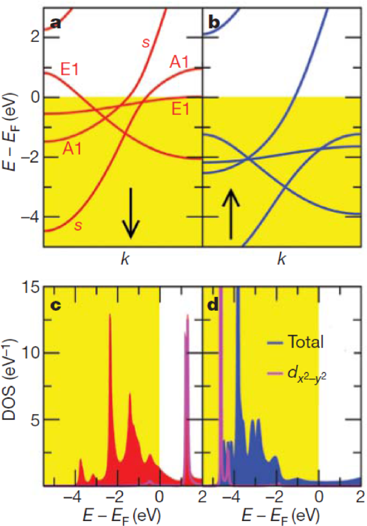
We modelled actual nanocontacts with two identical pyramids facing each other in the direction. As previously done for chainsWierzbowska et al. (2005), and to avoid the self-interaction problem, we computed the electronic structure of the nanocontact using LSDA+U. In Fig. 4c, d, we show the total density of states (DOS) projected on a tip atom and the DOS projected on the corresponding orbitals for both the minority (Fig. 4c) and the majority (Fig. 4d) spins (here we have set =3 eV). In general, solutions obtained for values of ranging from 3 to 5 eV also show that the orbital, forming one of the E2 bands in chains, hosts an integer local magnetic moment. Different geometries may favour the formation of the local moment in other strongly localized orbitals. The hybridization of the orbital with the surrounding orbitals results in antiferromagnetic kinetic exchange Schrieffer and Wolff (1966). We estimate that 1 eV, taking 5 eV, 2 eV and 8 eV from our LSDA+U calculations, where is the spin splitting of the orbital (Supplementary Information). We note that, in contrast to the contact atom(s), the intra-atomic hybridization vanishes for bulk atoms owing to the very small anisotropy of the crystal environment. This makes the antiferromagnetic coupling larger in the contact than in the bulk. This coupling competes with the ferromagnetic coupling , which we estimate from the splitting of the band at the boundary of the Brillouin zone for chains to be 0.2 eV (Fig. 4a, b). Thus, an overall antiferromagnetic coupling between electrons and conduction electrons is possible in nickel nanocontacts. Additionally, the local moment, m, responsible for the Kondo effect is subject to the ferromagnetic coupling to the neighbouring atoms, and this interaction also competes with the antiferromagnetic coupling:
| (2) |
Here the mi are the local moments of the neighbouring atoms and is the spin of the electrons. In ref. Pajda et al. (2001), the coupling was calculated for iron, cobalt and nickel by implementing the magnetic force theorem with a LSDA ground state. This method yields values for the spin-wave dispersion of the materials that compare well with experiment Mook and Paul (1985), and gives =19 meV, 15 meV and 2.7 meV for iron, cobalt and nickel, respectively. Thus, is significantly smaller than .
The Kondo effect in nanocontacts is favoured by three factors. First, a local moment forms in the contact atoms because of their smaller coordination. Second, the reduced symmetry of the contact, compared with the bulk, enhances the intra-atomic contribution to the hybridization and, thus, the antiferromagnetic coupling . Third, the smaller coordination also reduces the influence of the direct ferromagnetic coupling with neighbouring atoms. As a result, the local moment formed in the contact is antiferromagnetically coupled to the sp itinerant electrons and results in the Kondo effect in this system, in contradiction to conventional wisdom.
Acknowledgements.
We thank to E. Tosatti, R. Aguado and J. Ferrer for discussions, G. Scott and G. Saenz-Arce for experimental support and V. Esteve for technical support. This work was partly supported by the European Union through MolSpinIQ and Spanish MEC (grants MAT2007-65487, 31099-E and CONSOLIDER CSD2007-0010). D.J. acknowledges funding by the US National Science Foundation (NSF) under grant DMR-0528969. D.N. acknowledges the support of NSF grant DMR-0347253, the David and Lucille Packard Foundation and the W.M. Keck Program in Quantum Materials.Appendix A Methods
For the statistical results on the Kondo parameters, we used a home-made STM at 4.2K to fabricate the contacts by indentation between two pieces of metal Agraït et al. (2003). For the temperature-dependence measurements, the contacts were produced by the controlled electromigration at 4.2K of 100-nm-wide junctions fabricated by electron beam lithography Keane et al. (2006). In both cases, the spectroscopic curves were obtained by the addition of an a.c. voltage with a peak-power amplitude of 1mV and a frequency of 1 kHz to the d.c. bias voltage to allow the lock-in detection of the differential conductance.
Fabrication of atomic-scale contacts by scanning tunnelling microscopy.
Two pieces of metal wire of 0.1-mm diameter were cleaned and sonicated in acetone and isopropanol. These pieces were mounted in a home-built STM. The set-up was pumped down to high vacuum and immersed in a liquid helium bath until the temperature reached 4.2 K. The two pieces of wire were brought into contact and then pulled apart until the contact was of atomic dimension and, finally, until only one atom formed the contactAgraït et al. (2003). Strong indentation before the formation of every contact ensured the cleanliness of the atomic contacts. The histograms obtained by this technique (Fig. 1a) show similar results to the ones obtained by the mechanically controlled break junction technique, where the surfaces brought into contact are created under cryogenic conditions.
Fabrication of atomic-scale contacts using EBJs.
As a first step, a small junction about 100 nm wide was fabricated from cobalt using electron beam lithography and electron beam evaporation over a silicon dioxide substrate. To make the junction suitable for contact by macroscopic probes, two gold electrodes are deposited over the edges of the junction in a second lithography step, following the procedure described in ref. Keane et al. (2006). The samples are then placed in a probe station that was pumped down and immersed in a liquid helium bath until the sample reached a temperature close to 4.2 K. Under these conditions, the controlled electromigration process Park et al. (1999); Keane et al. (2006) was performed, decreasing the size of the junction to the atomic scale.
Appendix B Supplementary information on LSDA and LSDA+U results
The electronic structure of a Ni nanocontact model as that shown in Fig. 5 has been calculated with density functional theory in the local spin-density approximation (LSDA)Kohn and Sham (1965)using our established ab-initio transport methodology Jacob et al. (2005). Fig. 5a shows the DOS and partial DOS for one of the tip atoms of the nanocontact. The majority-spin -levels are completely filled while the minority-spin -levels are partially occupied with an average occupation of 0.8. This results in a net magnetic moment of 1 for the tip atom similar to the magnetic moment of the one-dimensional chain.
It is, however, well known that LSDA suffers from the so-called self-interaction problem which blue-shifts occupied levels. Here the spurious self-interaction brings all the minority -orbitals up to the Fermi level leading to a partial and almost equal occupation of 0.8 of all five -orbitals. The self-interaction error of LSDA is corrected, e.g., in the LSDA+U method Anisimov et al. (1991). In the LSDA+U method the effective LSDA Kohn-Sham potential of the strongly interacting -electrons is corrected by adding a Hartree-Fock term for an on-site Coulomb repulsion and exchange interaction :
| (3) |
Here, is the total occupation of all the -levels of an atom while is the occupation of an individual -level per spin , and is the total occupation of -levels per spin . accounts for the fact that the Coulomb repulsion and exchange interaction have already been taken into account in some way at the LSDA level, and thus have to be subtracted from the effective LSDA Kohn-Sham potential in order to avoid double-counting Anisimov et al. (1991).
Due to the low coordination of the two tip atoms (compared to the rest of the nanocontact and to bulk atoms) Coulomb interaction effects are expected to be much stronger for the tip atoms than for the rest of the nanocontact. Hence, we only treat the two tip atoms of the nanocontact at the LSDA+U level while the rest of the nanocontact is treated at the LSDA level. For bulk Ni a widely accepted value is =3 eV for the direct Coulomb repulsion and =1eV for the exchange interaction Grechnev et al. (2007). Due to the lower coordination of the tip atoms with respect to bulk atoms, the screening of the Coulomb repulsion should be lower than in bulk. Therefore the Coulomb repulsion is expected to be bigger than =3 eV for the tip atoms.
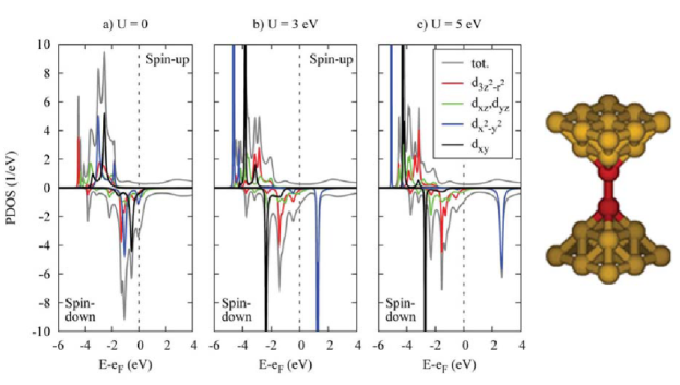
Indeed, as can be seen from Figs. 5a,b, for 3 eV four of the minority -orbitals are now well below the Fermi energy and completely occupied, while the minority −orbital is completely empty. Thus the magnetic moment of the tip atom is now entirely carried by the -level. This shows that a local moment can form on the tip atom which is carried by a single -orbital. The screening of the magnetic moment of this -orbital by the -conduction electrons can thus give rise to a Kondo resonance at the Fermi level.
| U | |||||
|---|---|---|---|---|---|
| 3 eV | 0.3 eV | 0.6 eV | -4.5 eV | 1.5 eV | 1.6eV |
| 5 eV | 0.3 eV | 0.6 eV | -5 eV | 3 eV | 1.0eV |
Now we estimate the exchange coupling of the −orbital of the tip atoms from the hoppings and excitation energies of the effective Hamiltonian of the LSDA+U calculation. The -orbital of the tip atom of one of the pyramids is coupled via hoppings and to the and -orbitals of the four atoms next to the tip atom in the same pyramid as detailed in Tab. 1. The total antiferromagnetic exchange coupling is given by:
| (4) |
where is the effective total hybridization with the -channels:
| (5) |
References
- Kondo (1964) J. Kondo, Prog. Theor. Phys. 32, 37 (1964).
- Fano (1961) U. Fano, Phys. Rev. 124, 1866 (1961).
- Goldhaber-Gordon et al. (1998) D. Goldhaber-Gordon, H. Shtrikman, D. Mahalu, D. Albusch-Madger, U. Meirav, and M. A. Kastner, Nature 391, 156 (1998).
- Cronenwett et al. (1998) S. M. Cronenwett, T. H. Oosterkamp, and L. P. Kouwenhoven, Science 281, 540 (1998).
- Park et al. (2002) J. Park, A. N. Pasupathy, J. I. Goldsmith, C. Chang, Y. Yaish, J. R. Petta, M. Rinkoski, J. P. Sethna, H. D. Abruña, P. L. McEuen, et al., Nature 417, 722 (2002).
- Liang et al. (2002) W. Liang, M. P. Shores, M. Bockrath, J. R. Long, and H. Park, Nature 417, 725 (2002).
- Nygard et al. (2000) J. Nygard, D. H. Cobden, and P. E. Lindelof, Nature 408, 342 (2000).
- Yu and Natelson (2003) L. H. Yu and D. Natelson, Nano Lett. 4, 79 (2003).
- Mandhavan et al. (1998) V. Mandhavan, W. Chen, T. Jamneala, M. F. Crommie, and N. S. Wingreen, Science 280, 567 (1998).
- Li et al. (1998) J. Li, W. D. Schneider, R. Berndt, and B. Delley, Phys. Rev. Lett. 80, 2893 (1998).
- Néel et al. (2007) N. Néel, J. Kröger, L. Limot, K. Palotas, W. A. Hofer, and R. Berndt, Physical Review Letters 98, 016801 (2007).
- Hewson (1993) A. C. Hewson, The Kondo problem to heavy fermions (Cambridge University, Cambridge, 1993).
- Agraït et al. (2003) N. Agraït, A. Levy-Yeyati, and J. M. van Ruitenbeek, Physics Reports 377, 81 (2003).
- Park et al. (1999) H. Park, A. K. L. Lim, A. P. Alivisatos, J. Park, and P. L. McEuen, Applied Physics Letters 75, 301 (1999).
- Untiedt et al. (2004) C. Untiedt, D. M. T. Dekker, D. Djukic, and J. M. van Ruitenbeek, Phys. Rev. B 69, 081401 (2004).
- Jacob et al. (2005) D. Jacob, J. Fernández-Rossier, and J. J. Palacios, Physical Review B 71, 220403 (2005).
- Calvo et al. (2008) M. R. Calvo, D. Jacob, M. J. Caturla, C. Untiedt, and J. J. Palacios, IEEE Transactions in Nanotechnology 7, 165 (2008).
- Jamneala et al. (2000) T. Jamneala, V. Madhavan, W. Chen, and M. F. Crommie, Phys. Rev. B 61, 9990 (2000).
- Keane et al. (2006) Z. K. Keane, L. H. Yu, and D. Natelson, Applied Physics Letters 88, 062514 (pages 3) (2006).
- van der Wiel et al. (2000) W. G. van der Wiel, S. D. Franceschi, T. Fujisawa, J. M. Elzerman, S. Tarucha, and L. P. Kouwenhoven, Nature 289, 2105 (2000).
- Hauptmann et al. (2008) J. R. Hauptmann, J. Paaske, and P. Lindelof, Nat. Phys. 4, 373 (2008).
- Martinek et al. (2003) J. Martinek, Y. Utsumi, H. Imamura, J. Barnaś, S. Maekawa, J. König, and G. Schön, Phys. Rev. Lett. 91, 127203 (2003).
- Martinek (2003) J. e. a. Martinek, Phys. Rev. Lett. 91, 247202 (2003).
- Choi et al. (2004) M.-S. Choi, D. Sánchez, and R. López, Phys. Rev. Lett. 92, 056601 (2004).
- Anderson (1961) P. W. Anderson, Phys. Rev. 124, 41 (1961).
- Schrieffer and Wolff (1966) J. Schrieffer and P. A. Wolff, Phys. Rev. 149 (1966).
- Wierzbowska et al. (2005) M. Wierzbowska, A. Delin, and E. Tosatti, Physical Review B (Condensed Matter and Materials Physics) 72, 035439 (2005).
- Pajda et al. (2001) M. Pajda, J. Kudrnovský, I. Turek, V. Drchal, and P. Bruno, Phys. Rev. B 64, 174402 (2001).
- Mook and Paul (1985) H. A. Mook and D. M. Paul, Phys. Rev. Lett. 54, 227 (1985).
- Kohn and Sham (1965) W. Kohn and L. J. Sham, Phys. Rev. 140, A1133 (1965).
- Anisimov et al. (1991) V. I. Anisimov, J. Zaanen, and O. K. Andersen, Phys. Rev. B 44, 943 (1991).
- Grechnev et al. (2007) A. Grechnev, I. D. Marco, M. I. Katnelson, A. I. Lichtenstein, J. Wills, and O. Eriksson, Phys. Rev. B 76, 035107 (2007).