Carbon nanotubes on partially depassivated n-doped Si(100)-(21):H substrates
Abstract
We present a study on the mechanical configuration and the electronic properties of semiconducting carbon nanotubes supported by partially depassivated silicon substrates, as inferred from topographic and spectroscopic data acquired with a room-temperature ultrahigh vacuum scanning tunneling microscope and density-functional theory calculations. A mechanical distortion and doping for semiconducting carbon nanotubes on Si(100)-(21):H with hydrogen-depassivated stripes up to 100 Å wide are ascertained from both experiment and theory. The results presented here point towards novel and local functionalities of nanotube-semiconductor interfaces.
pacs:
73.22.-f, 81.07.-b, 68.37.Ef, 68.43.-hThe modifications of the intrinsic electronic and thermal properties of single-walled carbon nanotubes (SWNTs) due to their interaction with the semiconducting surface by which they are supported have been the focal point of a sizeable number of experimentalHertel et al. (1998); Albrecht and Lyding (2003); Ruppalt et al. (2004); Albrecht and Lyding (2007a); Stobbe et al. (2006); Albrecht et al. (2007a); et al. (2008); Albrecht and Lyding (2007b); Albrecht et al. (2007b) and theoreticalAlbrecht et al. (2007a); Orellana et al. (2003); Miwa et al. (2005); Barraza-Lopez et al. (2006); Donadio and Galli (2007) studies in recent years due to the technological interest in hybrid SWNT-semiconductor devices. Dry contact transfer (DCT)Albrecht and Lyding (2003) allows for the in situ deposition of SWNTs from solid sources onto technologically relevant surfaces, such as Si(100)Albrecht and Lyding (2003, 2007a); Albrecht et al. (2007a); Albrecht and Lyding (2007b); Albrecht et al. (2007b) and the (110) surfaces of GaAs and InAsRuppalt et al. (2004), forming an atomically pristine interface. Comprehensive studies of semiconducting SWNTs (s-SWNTs) on Si(100) and Si(100)-(21):H at the density-functional theory (DFT) level have been reportedBarraza-Lopez et al. (2006); Albrecht et al. (2007a). The adsorption properties of s-SWNTs and metallic SWNTs (m-SWNTs) of similar diameter on Si(100) are remarkably differentBarraza-Lopez et al. (2006). This holds for 10 Å-diameter SWNTs with varying chiralities. Unlike m-SWNTs on Si(100), no covalent bonds are formed at the interface between Si(100) and s-SWNTs. (In recent studies of a (10,0) semiconducting SWNT on Si(100), covalent bonds between the s-SWNT and Si surface atoms were artificially inducedDonadio and Galli (2007) .) Si-C covalent bonding for SWNTs grown on Si was asserted only for a subset of the population based upon micro-Raman imaginget al. (2008), suggesting that both the electronic character of the SWNT and the local termination of the Si surface markedly influence the degree of nanotube-substrate interaction. When SWNTs are placed on the inert monohydride Si(100)-(21):H surfaceAlbrecht and Lyding (2003), the respective electronic characteristics of the nanotube and the surface are preserved and charge transfer is largely suppressedAlbrecht et al. (2007a); Miwa et al. (2005). In contrast, a shift of the Fermi level away from the nanotube midgap position has been experimentally observed for SWNTs supported by metallic surfaces (Au(111)DekkerLieber and Ag(100)Kawai ), unpassivated III-V compound semiconductors (GaAs(110) and InAs(110)Ruppalt et al. (2004)) and an ultrathin insulating film (NaCl(100)/Ag(100)Kawai ). Faithful to experimental conditions, our computational studies included dopants within the Si(100) slab. Ultrahigh vacuum scanning tunneling microscope (UHV-STM) based nanolithography on hydrogen-passivated Si(100) enables the definition of patterns of reactive depassivated SiShen et al. (1995); Foley et al. (1998) with possible consequences for the adhesion and electronic properties of the adsorbed SWNTsAlbrecht and Lyding (2007a); Albrecht and Lyding (2007b); Albrecht et al. (2007b). In this Letter, we report on the properties of isolated s-SWNTs interfaced with nanoscale regions of selectively depassivated Si as determined from room-temperature UHV-STM measurements and DFT calculations.

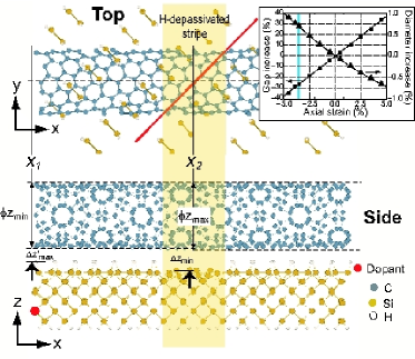
Fig. 1 summarizes the experimental observations; reproducible results were obtained for several unique s-SWNTs on partially depassivated Si(100)-(21):H. Degenerately -type doped Si(100) substrates (As, cm-3) were employed, and subjected to UHV H-passivationAlbrecht and Lyding (2003). Isolated HiPco SWNTsFN1 were deposited by DCT. The STM was operated at room temperature in constant-current mode with the bias voltage () applied to the substrate and the electrochemically etched W tip grounded through a current () preamplifier. Partial surface depassivation, as seen in the filled-states topograph of Fig. 1(a), was achieved with the methods described in Refs. Albrecht and Lyding, 2007b and Shen et al., 1995. Fig. 1(b) depicts the relative STM height along the top of the SWNT, as indicated by the blue line in Fig. 1(a). When the SWNT is on the H-passivated substrateAlbrecht and Lyding (2003) the height fluctuations are of the order of 0.2 Å, and they are directly related to the underlying honeycomb lattice of the SWNT. The dip in the apparent SWNT height stressed by the horizontal red line, beyond the 0.2 Å fluctuations, correlates with the location where the SWNT traverses the depassivated stripe (brighter region) in Fig. 1(a). Similar trends were reported beforeAlbrecht and Lyding (2007b). Given that the substrate is degenerately -doped, in the absence of a mechanical deformation, one would anticipate the negative charging of the Si surface states within the depassivated regionDujardin and a protrusion, rather than a dip, in the height profile: to maintain constant current, the tip should retract due to the higher density of states of the Si dangling bonds. Hence the data in Fig. 1(b) provides evidence for a slight conformal deformation (of the order of 0.5 Å) of the SWNT along the depassivated region. In a subsequent STM scan, the absolute current vs. bias was recorded ([] , = 20 mV) along the blue line in Fig. 1(c). In Fig. 1(c), we notice the apparent widening of the s-SWNT as the STM tip moves away from the depassivated region (the region within the two dashed vertical lines). This was previously observedAlbrecht et al. (2007b) and is consistent with the fact that the SWNT on Si(100)-(21):H only weakly interacts with the substrateAlbrecht et al. (2007a); Miwa et al. (2005). The d/d characteristics for the SWNT shown in Fig. 1(d) are consistent with those of a s-SWNT, as determined in Ref. Albrecht et al., 2007a. In Fig. 1(e), the absolute current vs bias, as a function of position along the SWNT, is shownFN2 . The white traces on Fig. 1(e) highlight the onset of the gap (upper and lower curves, at 1pA), as well as the midgap bias, equidistant from the conduction (upper) and valence (lower) band edges. The average onset biases are V and V, when an average is made from 0 to 150 Å; and V, for an average made from 150 to 250 Å in Fig. 1(e) (standard deviations are also indicated). The average values indicate a 0.06 V lowering of the band edges (and hence of the midgap) in the fully depassivated section. The presence of standard deviations of this order in our measurements at room temperature (the oscillations presented here are also seen at lower temperatures, see Ref. et. al. (2005)) calls for an independent confirmation of this effect from DFT calculations.
| Parameter | Undoped | -doped |
|---|---|---|
| 8.59 (3.0%) | 8.60 (3.1%) | |
| 8.63 (3.5%) | 8.47 (1.6%) | |
| 8.11 (2.8%) | 8.13 (2.5%) | |
| 8.09 (3.0%) | 8.22 (1.4%) | |
| 2.69 | 2.75 | |
| 1.96 | 1.94 |
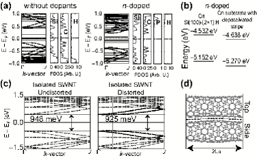
Calculations are performed for a (8,4) SWNT (diameter: 8.30 Å and length =11.29 Å). The supercell has six Si monolayers. The lowermost layer is passivated with H in the dihydride configurationNorthrup (1991). The uppermost Si layer is also H passivated, but in the monohydride configuration. The area spanned by the supercell is 43.2121.61 Å2. The supercell employed contains 1024 atoms when both Si surfaces are passivated with hydrogen, and 1012 atoms when a stripe of depassivated Si is formed. The SIESTA codeSoler et al. (2002) is employed in the local density approximation (LDA) for exchange-correlation as parametrized by Perdew and ZungerPerdew and Zunger (1981) from the Ceperley-Alder dataCeperley and Alder (1981). Double- plus polarization numerical atomic orbitals were used to expand the electronic wavefunctions, and a mesh cutoff of 220 Ry was employed to compute the overlap integrals. Si dimer rows form an angle of 45o with respect to the direction, as seen in Fig. 2. A section 10 Å wide (yellow rectangle in Fig. 2) is rendered chemically reactive by the removal of H atoms. Afterwards, the SWNT is placed on this substrate, crossing the depassivated section. A single phosphorous atom in the slab provides an -type doping density of 1020cm-3. Due to the lack of covalent bonding we find between s-SWNTs and Si(100), a better functional (i.e, that found in Ref. Dion et al. (2004)) should in principle be used. We choose LDA as it well describes (by cancellation of errors) the spacing between the s-SWNT and Si(100) better than GGA functionalsNicksuggestion . No corrections for basis set superposition error were added either. More details of the calculations can be found in Ref. Barraza-Lopez et al., 2006. Commensurability of the system required a non-negligible longitudinal contraction of the SWNT by 3.8%. As seen in the inset in Fig. 2, this entails a reduction of 30% in the semiconducting gap, and an increase in diameter by 0.75% to minimize the additional forces caused by the longitudinal contractionFN3 . The entire system shown in Fig. 2 was relaxed employing only the point until individual forces did not exceed 0.04 eV/Å. Because of periodic boundary conditions, the hydrogen stripe appears along the SWNT axis multiple times. This is to be contrasted with experiment, where a single stripe is fabricated. The SWNT displays a periodic distortion: it appears oblate with its maximum distortion occurring at and (Fig. 2). At , the major axis is parallel to the direction; while at it is the minor axis that is parallel to the direction. The reason for the distortion is that the SWNT bends towards surface depassivated Si atoms; to relieve the most stress, this vertical elongation is accompanied by a horizontal elongation at the edges of the unit cell. The Si atoms in the depassivated section also protrude towards the SWNT. Specific values are in Table I. Although smaller than experimental values in magnitude, the DFT results are consistent with a mechanical distortion of the SWNT caused by the substrate (in simulations the depassivated stripe is 10 Å wide; in experiment it is about 100 Å wide). The resulting band structure, computed with a 441 Monkhorst-Pack point meshMonkhorst and Pack (1976), with and without dopants is given in Fig. 3(a). Flat bands are due to dangling bonds in Si atoms which pin the Fermi level. The projected density of states (PDOS) of C atoms is highlighted in Fig. 3(a). For an undoped substrate, electrons from the periphery of the SWNT escape to the substrate, and as a result the SWNT becomes -doped as the carbon HOMO level moves upward towards the Fermi energy (see also Ref. Barraza-Lopez et al., 2006). Upon -doping of the Si substrate, the location of the carbon band edges in Fig. 3(a) moves downwards with respect to the system’s Fermi level, as the Coulomb repulsion caused by excess electrons in the substrate suppress to some extent electron transfer from the SWNT.
In order to provide theoretical support to the lowering of the band edges when the substrate is locally depassivated, the PDOS for the SWNT on a doped substrate with full H-coverage on its upper surface was obtained. (In this case, no further relaxation to the fully passivated H substrate was performed upon placement of the dopant atom.) The location of the SWNT conduction and valence band edges are shown in Fig. 3(b). It can be seen that the band edges shift down by 0.11 eV when the H-depassivated strip is present. The larger value than the one found in experiment may be due to the fact that in calculations the depassivated strip repeats infinitely along the nanotube’s length. Discrepancies may also be due to the approximations in the calculations. (The change in the nanotube band gap of about 10 meV lays within our precision in computing the PDOS). A similar calculation was performed for the case when the substrate was undoped. In that case the band edges remained in their original positions even when the depassivated strip was present: The band edges in this latter case were at () eV and () eV on the full H-passivated (partially depassivated) systems.
The mechanical distortion in the SWNT and its relation to the electronic band structure can be understood by introducing a parametric distortion along the and directions to an uncompressed, isolated SWNT:
| (1) |
() are the coordinates of an undistorted, uncompressed SWNT. Eq. (1) implies a periodicity in the direction over two SWNT unit cells, aimed to reduce the local distortion for C atoms, while keeping a relatively small supercell. The dissimilar amplitude of the modulation along the and directions is responsible for the lifting of the degeneracy at points, highlighted by horizontal arrows in Fig. 3(a), n-doping and Fig. 3(c). This parametric distortion results in a modest reduction of the semiconducting gap, also consistent with results from full-scale calculations (Fig. 3(a)). Fig. 3(d) schematically depicts the shape of the SWNT after a distortion as that shown in Eq. (1) is applied. The distortion also results in a shift of the nanotube’s conduction and valence band edges away from the point, as is the case in Fig. 3(a).
In conclusion, it has been shown from STM data and DFT calculations that partial depassivation of degenerately doped Si(100)-(21):H produces a mechanical distortion within an adsorbed s-SWNT that slightly modifies the magnitude of the semiconducting gap, and produces minor modifications to the band structure of the nanotube. More importantly, the partial depassivation allows for a slight local doping of the SWNT adsorbed on this substrate. We expect that an increase in the area of the clean stripe will result in a further population of electronic states at the Si(100)-SWNT interface, until the behavior described in Ref. Barraza-Lopez et al., 2006 is recovered. We thank M. Kuroda, N. A. Romero and K. Ritter for discussions. Calculations were performed on the Turing cluster and the Intel-64 Abe cluster at U of I. Support by the NCSA (grants TG-PHY090002 and TG-PHY090034) is acknowledged.
References
- Hertel et al. (1998) T. Hertel, R. E. Walkup, and P. Avouris, Phys. Rev. B 58, 13870 (1998).
- Albrecht and Lyding (2003) P. M. Albrecht and J. W. Lyding, Appl. Phys. Lett. 83, 5029 (2003).
- Albrecht and Lyding (2007a) P. M. Albrecht and J. W. Lyding, Small 3, 146 (2007a).
- Albrecht et al. (2007a) P. M. Albrecht, S. Barraza-Lopez, and J. W. Lyding, Nanotechnology 18, 095204 (2007a).
- Ruppalt et al. (2004) L. B. Ruppalt, P. M. Albrecht, and J. W. Lyding, J. Vac. Sci. Technol. B 22, 2005 (2004); L. B. Ruppalt and J. W. Lyding, Nanotechnology 18, 215202 (2007).
- Stobbe et al. (2006) A. Jensen, J. R. Hauptmann, J. Nygard, J. Sadowski, and P. E. Lindelof, Nano Lett. 4, 349 (2004); S. Stobbe, P. E. Lindelof, and J. Nygard, Semicond. Sci. Technol. 21, S10 (2006); C.-W. Liang and S. Roth, Nano Lett. 8, 1809 (2008).
- et al. (2008) Y. M. You, T. Yu, J. Kasim, H. Song, X. F. Fan, Z. H. Ni, L. Z. Cao, H. Jiang, D. Z. Shen, J. L. Kuo, and Z. X. Shen, Appl. Phys. Lett. 93, 103111, (2008).
- Albrecht and Lyding (2007b) P. M. Albrecht and J. W. Lyding, Nanotechnology 18, 125302 (2007b).
- Albrecht et al. (2007b) P. M. Albrecht, S. Barraza-Lopez, and J. W. Lyding, Small 3, 1402 (2007b).
- Orellana et al. (2003) W. Orellana, R. H. Miwa, and A. Fazzio, Phys. Rev. Lett. 91, 166802 (2003); Y.-H. Kim, M. J. Heben, and S. B. Zhang, Phys. Rev. Lett. 92, 176102 (2004); S. Berber and A. Oshiyama, Phys. Rev. Lett. 96, 105505 (2006); J.-Y. Lee and J.-H. Cho, Appl. Phys. Lett. 89, 023124 (2006); G. W. Peng, A. C. H. Huan, R. Q. Wu, L. Liu, and Y. P. Feng, Phys. Rev. B 74, 235416 (2006); W. Orellana, Appl. Phys. Lett. 92, 093109 (2008); L. Yan, Q. Sun, and Y. Jia, J. Phys.: Condens. Matter 20, 225016 (2008).
- Miwa et al. (2005) R. H. Miwa, W. Orellana, and A. Fazzio, Appl. Phys. Lett. 86, 213111 (2005).
- Barraza-Lopez et al. (2006) S. Barraza-Lopez, P. M. Albrecht, N. A. Romero, and K. Hess, J. Appl. Phys. 100, 124304 (2006).
- Donadio and Galli (2007) D. Donadio and G. Galli, Phys. Rev. Lett. 99, 255502 (2007). Results of this work apply to metalic SWNTs, which do form covalent bonds to Si(100).
- (14) J. W. G. Wildoer, L. C. Venema, A. G. Rinszler, R. E. Smalley and C. Dekker, Nature 391, 59 (1998); T. W. Odom et al., Nature 391, 62 (1998).
- (15) H.-J. Shin, S. Clair, Y. Kim, and M. Kawai, Appl. Phys. Lett. 93, 233104 (2008).
- Shen et al. (1995) J. W. Lyding, T.-C. Shen, J. S. Hubacek, J. R. Tucker, and G. C. Abeln, Appl. Phys. Lett. 64, 2010 (1994).
- Foley et al. (1998) T.-C. Shen, C. Wang, G. C. Abeln, J. R. Tucker, J. W. Lyding, Ph. Avouris, and R. E. Walkup, Science 268, 1590 (1995).
- (18) Carbon Nanotechnologies, Inc., Houston, Texas.
- (19) M. Lastapis, M. Martin, D. Riedel, and G. Dujardin, Phys. Rev. B 77, 125316 (2008).
- (20) The data is filtered below 1 pA, which is about a factor of two above the noise floor resulting from the tunneling preamplifier gain setting of V/A.
- et. al. (2005) S. Lee, G. Kim, H. Kim, B.-Y. Choi, J. Lee, B. W. Jeong, J. Ihm, Y. Kuk, and S.-J. Kahng, Phys. Rev. Lett. 95, 166402 (2005).
- Northrup (1991) J. E. Northrup, Phys. Rev. B 44, 1419 (1991).
- Soler et al. (2002) J. M. Soler, E. Artacho, J. D. Gale, A. García, J. Junquera, P. Ordejón, and D. Sánchez-Portal, J. Phys.: Condens. Matter 14, 2745 (2002).
- Perdew and Zunger (1981) J. P Perdew and A. Zunger, Phys. Rev. B 23, 5048 (1981).
- Ceperley and Alder (1981) D. M. Ceperley and B. J. Alder, Phys. Rev. Lett. 45, 566 (1980).
- Dion et al. (2004) M. Dion, H. Rydberg, E. Schröder, D. C. Langreth, and B. I. Lundqvist, Phys. Rev. Lett. 92, 246401 (2004).
- (27) R. Armiento and A. E. Mattsson, Phys. Rev. B 72, 085108 (2005).
- (28) The effect of axial strain on the electronic structure of SWNTs has been addressed beforeHeyd et al. (1997); Yang and Han (2000). We placed a (8,4) SWNT on a unit cell of dimensions 20Å20Å ( varying from % to %). Upon strain, the SWNT is let to relax until forces do not exceed 0.01 eV/Å. As a result, the SWNT diameter increases (decreases) as it is longitudinally compressed (elongated).
- Monkhorst and Pack (1976) H. J. Monkhorst and J. D. Pack, Phys. Rev. B 13, 5188 (1976).
- Heyd et al. (1997) R. Heyd, A. Charlier, and E. McRae, Phys. Rev. B 55, 6820 (1997).
- Yang and Han (2000) L. Yang and J. Han, Phys. Rev. Lett. 85, 154 (2000).