Interfaces Within Graphene Nanoribbons
Abstract
We study the conductance through two types of graphene nanostructures: nanoribbon junctions in which the width changes from wide to narrow, and curved nanoribbons. In the wide-narrow structures, substantial reflection occurs from the wide-narrow interface, in contrast to the behavior of the much studied electron gas waveguides. In the curved nanoribbons, the conductance is very sensitive to details such as whether regions of a semiconducting armchair nanoribbon are included in the curved structure – such regions strongly suppress the conductance. Surprisingly, this suppression is not due to the band gap of the semiconducting nanoribbon, but is linked to the valley degree of freedom. Though we study these effects in the simplest contexts, they can be expected to occur for more complicated structures, and we show results for rings as well. We conclude that experience from electron gas waveguides does not carry over to graphene nanostructures. The interior interfaces causing extra scattering result from the extra effective degrees of freedom of the graphene structure, namely the valley and sublattice pseudospins.
pacs:
73.63.Nm, 73.21.Hb, 73.23.Ad, 73.61.Wp,
1 Introduction
There has been tremendous interest recently in investigating carbon-based nanoelectronics, first with carbon nanotubes [1, 2, 3] and more recently with graphene [4]. In that context, researchers have intensively studied graphene “nanoribbons” – infinite, straight strips of graphene of constant width – both theoretically [5, 6, 7, 8, 9, 10, 11, 12, 13, 14, 15, 16, 17, 18, 19, 20, 21, 22, 23] and experimentally [24, 25, 26, 27, 28, 29, 30, 31]. Most of the theoretical effort has been focused on nanoribbons of essentially constant width. However, more functionality, beyond that of a mere wire, might be gained if one considers more general and realistic nanoribbons in which the width of the ribbon changes, it curves, or particular junctions of nanoribbons are formed.
On a more fundamental level, the continuing great interest in the effect of reduced dimensionality, such as electron-electron interactions in reduced dimensions, provides motivation for studying quasi-one-dimensional systems. Graphene’s unusual dispersion (massless Dirac fermions) and reduced density of states at the Fermi energy, for instance, suggest potential for novel effects. Of course, one should first understand the non-interacting system before turning to interactions.
Graphene nanoribbons are closely analogous to electron waveguides patterned out of two dimensional electron gas (2DEG), usually in GaAs or other semiconductor systems [32, 33, 34, 35, 36, 37, 38, 39, 40, 41, 42]. However, there is an important difference in how the confinement is achieved. While in 2DEG waveguides the electrons are trapped in the transverse direction of the waveguide by applying a potential by means of local gate electrodes, graphene nanoribbons are directly cut out of a larger graphene flake. This gives rise to different types of boundaries, depending on the direction in which the nanoribbons are cut with respect to the graphene lattice. If the longitudinal direction of the nanoribbon is along the direction of nearest neighbor carbon bonds, the resulting boundary is of “armchair” type, while cutting at with respect to the nearest neighbor carbon bonds results in a “zigzag” boundary (see figure 1). It has been shown that the low energy properties of nanoribbons with boundaries other than these two are equivalent to those of zigzag nanoribbons [43]. On the experimental side, there has been recent progress in controlling the edges of graphene samples [44, 45], which is essential to enable physicists to probe the influence of edge details on transport properties.
This paper is organized as follows: First we study one of the most simple systems beyond a straight nanoribbon with constant width, namely wide-narrow junctions, by which we mean two semi-infinite nanoribbons attached together to form a step. We calculate the conductance of such ribbons by numerically solving the tight binding model, and also obtain analytical results for the case of armchair boundaries. In the second part we investigate numerically the conductance of curved wires cut out of graphene. In this case the width of the nanoribbon is approximately constant, but the longitudinal direction with respect to the underlying graphene lattice and hence the transverse boundary conditions change locally. In contrast to systems with sharp kinks and abrupt changes in the direction, which have been investigated in earlier work [7, 13, 14, 19, 20, 21, 46], we focus here on smooth bends.
In both cases we find remarkable deviations from the conductance of 2DEG waveguides that are clear signatures of the sublattice and valley degrees of freedom in the effective 2D Dirac Hamiltionian describing graphene’s low energy excitations,
| (1) |
Here the matrix structure is in valley space, are Pauli matrices in pseudo- or sublattice- spin space, are the momentum operators, and m/s is the Fermi velocity. Alternatively, from a strictly lattice point of view, the deviations that we see are caused by the basis inherent in graphene’s hexagonal lattice.
For our numerical work, we use a nearest-neighbor tight binding model taking into account the -orbitals of the carbon atoms [4, 47] and solve the transport problem using an adaptive recursive Green function method [48] to obtain the conductance . Throughout the paper, lengths are given in units of the graphene lattice constant which is times the nearest-neighbor carbon-carbon length, while energies are in units of the nearest-neighbor hopping constant eV.
2 Wide-narrow junctions: Changing the width of a nanoribbon
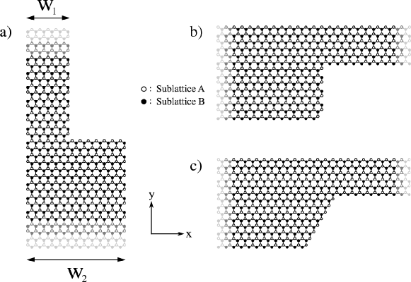
The simplest way to form an interface within a nanoribbon is to change its width. In this section we investigate the conductance of infinite nanoribbons in which the width changes from wide to narrow, which then can be viewed as a junction between a wide semi-infinite nanoribbon and a narrow one. Figure 1 shows three examples of such junctions with armchair (ac) and zigzag (zz) type edges. We denote the width of the narrower wire by and the width of the wider wire by . A naive expectation for the dependence of on the Fermi energy is the step function where is the number of occupied transverse channels in the narrow wire. This would be correct if there were no reflection at the wide-narrow interface. Realistically, however, there is scattering from this interface, and so the steps in the conductance are not perfectly sharp.
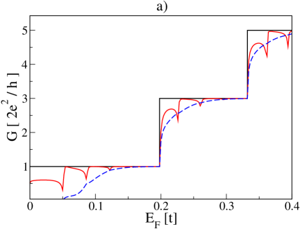
For usual 2DEGs modeled by either a square lattice of tight-binding sites or a continuum Schrödinger equation with quadratic dispersion, the detailed shape of has been studied previously. Szafer and Stone [36] calculated by matching the transverse modes of the two semi-infinite wires. The inset in figure 2 (b) compares tight-binding results (using a square grid) with mode-matching results in this case for in the one-mode regime of the narrow part. The agreement between the two is excellent. Note that the resulting conductance step is very steep.
2.1 Armchair nanoribbons

For armchair nanoribbons, the analysis proceeds in much the same way as for the usual 2DEG, square lattice case. At a fixed Fermi energy in the effective Dirac equation, the transverse wavefunctions for the various subbands are mutually orthogonal, as explained further in A. Performing a matching procedure similar to that used in Ref. [36], one calculates the conductance from the overlap of transverse wavefunctions on the two sides of the wide-narrow junction. A detailed derivation is presented in B.
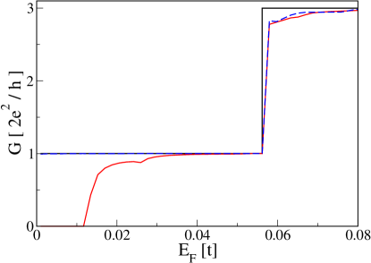
Figure 2 shows the conductance resulting from the numerical solution of the matching equations at energies for which there is one propagating mode in the narrow part. In addition, the conductance obtained from tight-binding calculations for wide-narrow junctions between armchair nanoribbons is shown (using the hexagonal graphene lattice). Figure 2 shows for different combinations of metallic and semiconducting nanoribbons (cf. A). The agreement between the two methods is extremely good: even the singularity associated with the subband threshold in the wider ribbon is reproduced in detail by the mode matching method, showing that the effective Dirac equation describes the system very well.
In figure 2, we see immediately that for the armchair nanoribbon case differs greatly from the normal 2DEG [inset of figure 2 (b)]: the rise from zero to unit conductance is much slower in graphene, taking at least half of the energy window and in some cases [see e.g. figure 2 (a)] not reaching the saturation value at all. For completely metallic nanoribbons, the lineshape is very different [panel (c)] and the conductance is suppressed at low Fermi energies (see also reference [49]).
2.2 Zigzag nanoribbons
For zigzag nanoribbons, the analysis does not proceed as simply as in the usual 2DEG or armchair nanoribbon cases: the transverse wavefunctions depend on the longitudinal momentum – similar to 2DEG wires with a magnetic field – and are not orthogonal at fixed Fermi energy (cf. A). Because this orthogonality is used in the matching method of B, we cannot apply it to the zigzag case.
Figure 3 (a) shows numerical tight binding results for in two different systems with zigzag edges: one with an abrupt change in width (red curve) and one with a gradual connection (blue curve), as depicted in figures 1 (b) and (c), respectively. Note first that the conductance is close to its maximum value only in small windows of energy, as in the armchair nanoribbon case and in marked contrast to the usual 2DEG, square lattice situation.
In the abrupt case, one sees pronounced antiresonances at the threshold energies for transverse modes in the wide nanoribbon. In order to see that this is due to the boundary conditions satisfied by the transverse modes in a zigzag nanoribbon, consider the following argument. As seen in Figures 1 (b) and (c), there is only one sublattice at each zigzag edge. In the effective Dirac equation one has a spinor with entries corresponding to the sublattices, thus the boundary condition is that one of the entries has to vanish at the edge while the other component is determined by the Dirac equation and is in general not zero at the boundary [9]. One finds from equation (25) (e. g. from a graphical solution) that the higher is above the threshold of a mode, the closer the transverse wavenumber gets to a multiple of and the closer the value of the spinor entry in question goes to zero. For our situation, then, the matching of a transverse mode in the narrow nanoribbon (which is already far above the threshold of the mode) with one in the wider nanoribbon is particularly bad at the threshold of the latter and gets better with increasing Fermi energy. This explains the observed antiresonances in .
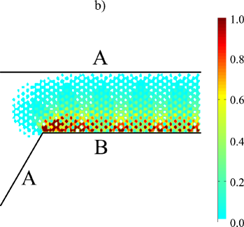
For the gradually widened junction, we insert another zigzag edge to interpolate between the wide and narrow nanoribbon [see figure 1 (c)]. In this case, the modes of the two infinitely extended parts are not directly matched and thus the sharp antiresonances are not present. Note, however, the complete suppression of at very low energies. In this regime there is only a single mode propagating in the wide nanoribbon as well as in the narrow one. This state is located mainly on the B sublattice close to the lower edge and on the A sublattice on the upper edge. Since the sublattice at the lower edge changes from A to B at the junction [cf. figure 1 (c)], this state cannot be transmitted and the conductance is zero. This is confirmed by the intensity distribution plotted in figure 3 (c). In the more realistic next-nearest-neighbor hopping model, the situation is the same for most of the single mode regime but changes for very low energies, when the so-called edge states are propagating [6, 9]. In that regime, the two states are exponentially localized at the upper and lower edge, respectively, and are independent of each other. Thus, the one localized at the A edge transmits whereas the one localized at the B edge is blocked [22].
Summarizing the results for the wide-narrow junctions, we see that the behavior of graphene nanoribbons differs substantially from that of the familiar 2DEG situation. The matching at the graphene junctions is much less good, leading to a suppression of the conductance from the expected nearly step-like structure.
3 Curved graphene nanoribbons
Curved nanoribbons are defined by cutting smooth shapes out of an infinite graphene sheet. Since the graphene lattice is discrete, the resulting boundary is not perfectly smooth but will have edges of zigzag and armchair type in certain directions as well as some intermediate edge types. However, according to Akhmerov and Beenakker [43], the intermediate boundary types behave basically like zigzag boundaries for low energies, and we thus call these boundaries “zigzag-like”.
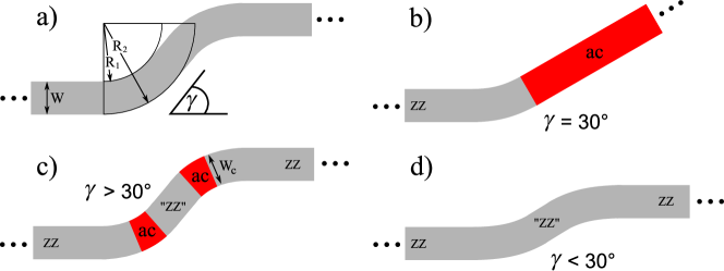
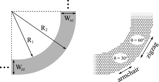
In figure 4 we show schematically several of the curved nanoribbons studied. A “sidestep nanoribbon” consists of an infinitely extended horizontal zigzag ribbon of width , followed by a curved piece with outer radius of curvature and inner radius , a second straight piece making an angle with respect to the first one, a curve in the opposite direction, and finally followed by another infinitely extended zigzag nanoribbon. The details of the system’s edge depend on : (1) If , the middle straight piece has armchair edges. (2) If the middle straight piece is zigzag-like with the dominating sublattice at the edges reversed from that for the two horizontal nanoribbons. In the curved part, there is a small region where the edges are locally of armchair type. If we denote the angle of the local longitudinal direction from the horizontal by , this happens at [see figure 4 (c)]. The inset in figure 5 shows the lattice structure of such a curved region. (3) Finally, if , the middle straight piece also has zigzag-like edges, but the dominating sublattice at the edges is the same as for the horizontal ribbons. In this case, no local armchair region forms as is always smaller than [see figure 4 (d)].
In these various cases, then, different interior interfaces are formed between zigzag and armchair nanoribbons. We will see that the type of interface is critical in determining the properties of the curved nanoribbons. In addition, the nature of the armchair nanoribbon – whether it is semiconducting or metallic – has a large effect on the conductance. Thus the width of the armchair region is an important parameter; according to equation (16) one has a metallic nanoribbon if and a semiconducting nanoribbon otherwise.
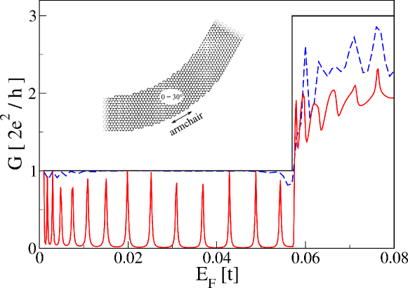
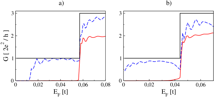
Figure 5 shows the conductance of sidestep nanoribbons with , for which a small armchair region is formed in each of the curved parts. When the width of this armchair region corresponds to a metallic nanoribbon, the conductance is basically – the maximum possible value – throughout the one-mode regime of the zigzag leads (, dashed blue line). In striking contrast, when the width is just larger (red line) the conductance is strongly suppressed. Resonance peaks result from Fabry-Perot behavior caused by scattering from the two armchair regions which define a “box” for the middle straight region. We find this behavior consistently for all sidestep wires in which armchair regions form that have a width corresponding to a semiconducting nanoribbon.
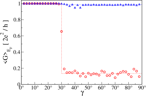
Figure 6 shows the dependence on the angle by plotting the conductance averaged over all energies for which there is one propagating mode in the zigzag leads. For there are no armchair regions in the curved parts of the structure, and the average conductance is very close to the maximum value in all cases studied. As soon as the critical angle of is surpassed and small armchair pieces form in the curves, the conductance depends strongly on the exact value of . If corresponds to a metallic ribbon, remains high and is rather independent of . On the other hand if corresponds to a semiconducting ribbon, suddenly drops by more than 80 percent and then remains approximately constant upon further increase of . The constancy of in the respective regimes supports the statement of Ref. [43] that straight boundaries that are neither exactly of armchair nor exactly of zigzag type behave like zigzag boundaries. To summarize, if a curve in a zigzag nanoribbon causes two semiconducting armchair regions to appear, then a very effective barrier is formed which causes very high reflectivity.

The simplest idea to explain this effect would be that at low energies there is by definition a gap in a semiconducting ribbon and since this means there are no propagating states in the local armchair region, one expects the conductance to be suppressed because electrons have to tunnel trough this region in order to be transmitted. However, this does not explain our findings: the energy range over which the conductance suppression occurs is much larger than the energy gap of the semiconducting region. In fact it is given by the energy range of the one-mode regime in the surrounding zigzag parts. To make this clear, we show the bandstructures of both a semiconducting armchair ribbon and a zigzag ribbon of approximately the same width in figure 7 (both nanoribbons are infinitely extended). One can clearly see that within the one-mode regime of the zigzag nanoribbon, in which the states are completely valley polarized, there can be several propagating modes in the semiconducting armchair nanoribbon, so the suppression of must be of a different origin.
Furthermore, it is not the bare zigzag-armchair junction that leads to suppressed conductance, but rather it is necessary to have two zigzag pieces differing by an angle of more than and being separated by a small armchair region. This can be seen in two stages. First, figure 8 shows the conductance of an infinitely extended zigzag nanoribbon connected to an infinitely extended armchair nanoribbon via a curve, the structure shown schematically in figure 4 (b). In the one-mode regime of the zigzag ribbon, the conductance is maximal for the case of a metallic armchair ribbon. For a semiconducting armchair ribbon, the conductance is, of course, zero for energies below the gap, but it increases rapidly up to for larger values of . Thus, a single zigzag to semiconducting-armchair interface conducts well.
For the second stage of the argument, consider a bend through from an infinite zigzag lead to an armchair one, as depicted in figure 9. In contrast to the zigzag-armchair connection just discussed, this one has three interfaces between zigzag and armchair regions. Figure 10 shows the conductance of several curved nanoribbons. As for the sidestep ribbons, the conductance is suppressed when a semiconducting armchair region is present in the curve. Note that the suppression is not due to the infinitely extended armchair lead, for which we chose a semiconducting nanoribbon in 10 (a) and a metallic one in 10 (b).
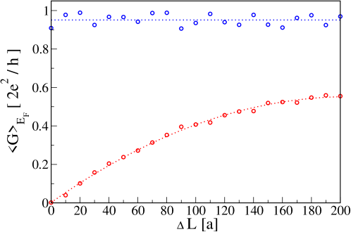
If one makes the natural assumption that the armchair region acts as a blocking barrier, one would expect the blocking to become more effective as the armchair region is lengthened. However, this is clearly not the case in the data shown in figure 11. The system is a curved nanoribbon in which the armchair region at is lengthened by ; we plot , the conductance averaged over all energies in the one-mode regime of the zigzag lead, as a function of . For a metallic armchair region in the curve, the conductance is roughly independent of , as expected. Surprisingly, for the semiconducting case, the conductance increases as a function of .This establishes, then, that conductance suppression occurs when two zigzag-armchair interfaces occur in close spatial proximity.
Our numerical results suggest that the evanescent modes in the armchair regions play an essential role. They are necessary, of course, in order to match the propagating zigzag mode to a solution in the armchair region. For short armchair pieces the evanescent modes from the two interfaces overlap. We conjecture that these evanescent modes are mutually incompatible in the semiconducting case, destroying the possibility of matching on both sides at the same time, while they are compatible for metallic armchair regions. If one has a long armchair piece, the evanescent modes decay leading to independent matching at the two ends.
4 Conclusions
We have shown in a variety of examples that interfaces within graphene nanoribbons can strongly affect their conductance, much more so than in the familiar 2DEG electron waveguides and wires. First, for wide-narrow junctions, our main results are figures 2 and 3. For both armchair and zigzag nanoribbons, changes in width act as a substantial source of scattering, reducing the conductance. Second, for curved nanoribbons, our main results are figures 6, 8, and 11. There is a strong reduction in conductance when a curve joining two zigzag regions contains a semiconducting armchair region.
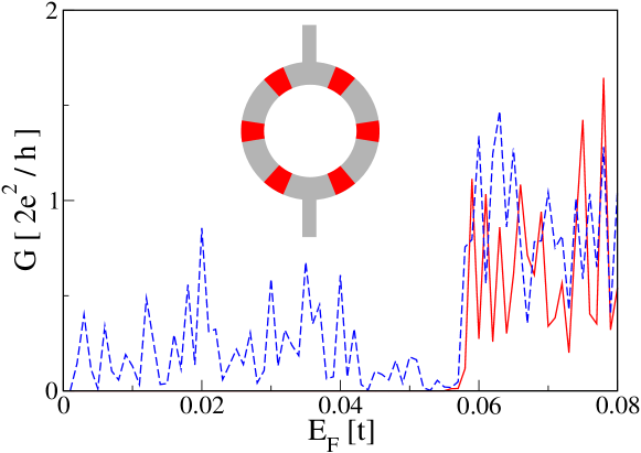
The effect of such internal interfaces will certainly be felt in more complex structures as well. As an example, consider rings for studying the modulation of the conductance by a magnetic field through the Aharonov-Bohm effect [50]. Figure 12 shows such a ring schematically together with its conductance in two cases. As for the curved nanoribbons, when semiconducting armchair regions occur in the curved part of the structure, the conductance is substantially reduced.
In considering experimental manifestations of internal interfaces, disorder, and in particular the edge disorder which has received attention recently [44, 45, 51, 52, 53, 54], may be important. The effects we observe in our calculations will most likely also be present in structures with disordered edges, provided the disorder is not too strong. Consider, for example, the suppression of the conductance in curved wires. In the inset of figure 5 as well as in figure 9, one can see that between the armchair and the zigzag regions, the edges are not perfect. We believe that when the edge disorder is weak enough to allow for pieces with armchair edges, the suppression should still be present.
The underlying reason for the impact of internal interfaces can be viewed in two ways. From the lattice point of view, it arises from the additional complexity of the hexagonal lattice with its basis compared to the standard square lattice. Equivalently, from the continuum point of view, it arises from the extra degrees of freedom inherent in the Dirac-like equation governing graphene – those of the sublattice and valley pseudospins. As development of graphene nanostructures accelerates, the impact of internal interfaces should be taken into account when considering future carbon nanoelectronic schemes.
Appendix A Wavefunctions of graphene nanoribbons in the Dirac equation
We calculate the eigenfunctions of graphene nanoribbons withing the effective Dirac model. This has been done by Brey and Fertig in [9] and Peres, et alin [10]. The effective Dirac equation taking into account contributions from both valleys is given by [4]
| (2) |
with
| (3) |
and
| (4) |
Here and are spinors with two components corresponding to contributions from the two different valleys and respectively. and are scalar wavefunctions, where the subscripts and stand for the two sublattices (see figure 13). The total wavefunction containing the fast oscillations from the -points is then
| (5) |
A.1 Armchair nanoribbons
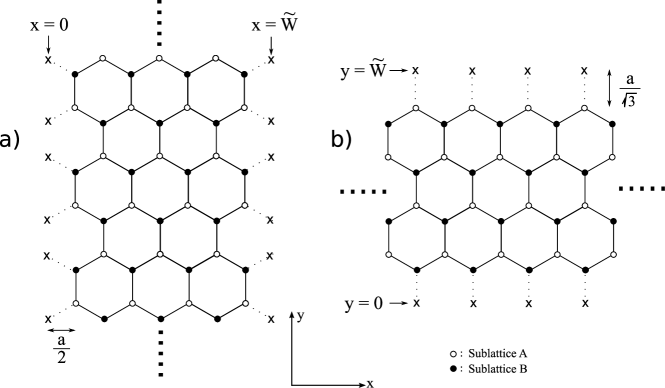
We consider an armchair nanoribbon which is infinitely extended along the -direction [see figure 13 (a)]. Using the Bloch ansatz
| (6) |
and the Dirac equation (2), one obtains
| (7) | |||
| (8) | |||
| (9) | |||
| (10) |
and, by applying the Hamiltonian twice,
| (11) |
with . According to figure 13 (a), the correct boundary condition [9] for an armchair nanoribbon is for and . (For the connection between the nanoribbon width used previously and , see the caption of figure 13.) The ansatz , solves both the B sublattice parts of equation (11) with and the boundary condition, if we require
| (12) |
where . We find that and . Using equations (7) and (9) to determine and from and , we thus find that, up to a normalization factor, the wavefunctions are
| (13) |
| (14) |
The wavefunction is, up to the spinor part, very similar to that of a 2DEG waveguide: the width of the ribbon is a multiple of half the transverse wavelength. However, here the transverse wavelength is of order the lattice constant, not the system’s width, since is of order for the energetically lowest lying modes. Nevertheless, the wavefunctions for different transverse quantum numbers are orthogonal at a fixed Fermi energy. Note that for evanescent modes we just have to consider imaginary wavenumbers and equations (12), (13), and (14) still hold.
The energy for this solution is
| (15) |
Therefore one has a metallic spectrum if there is a state with . From equation (12) it follows immediately that this is the case whenever
| (16) |
A.2 Zigzag nanoribbons
For a zigzag nanoribbon along the -direction [see figure 13 (b)], the Bloch ansatz is
| (17) |
the Dirac equation becomes
| (18) | |||
| (19) | |||
| (20) | |||
| (21) |
and one has
| (22) |
The boundary condition for a zigzag ribbon differs from that for an armchair ribbon in that the wavefunction has to vanish on only one sublattice at each edge [9]: . With the following ansatz for and ,
| (23) |
(22) yields , and the boundary condition requires and . Thus the valleys completely decouple for zigzag nanoribbons, and equations (19) and (21) yield
| (24) |
where for the and for the valley. The boundary condition for the parts of the wavefunction provides an equation that determines the allowed values for ,
| (25) |
Thus the transverse quantum number is coupled to the longitudinal momentum, as in 2DEG waveguides in the presence of a magnetic field. In order to write equation (24) in a symmetric way, we square the quantization condition (25) and use the relation to obtain
| (26) |
Using (25) and (26) in equation (24) leads to
| (27) |
with . ¿From this symmetric expression, one clearly sees that the total weight on each sublattice is the same.
The transcendental equation (25) has real solutions only for . These states correspond to bulk states: they are extended over the whole width of the ribbon. For there are only imaginary solutions , corresponding to the so-called edge states [6, 9], which are exponentially localized at the edges and live predominantly on one sublattice at each side, as can be seen from equation (24). For the special case corresponding to equation (27) results in
| (28) |
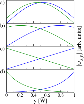
i. e. a linear profile of the transverse wavefunction. Figure (14) shows the profile of several transverse zigzag modes.
Appendix B Mode matching for wide-narrow junctions with armchair edges
We derive a set of analytic equations that determine the transmission amplitudes for wide-narrow junctions with armchair edges as introduced in section 2.1. We label the transverse modes in the narrow part of the system by and those in the wide part by . The stands for propagation in positive and negative -direction respectively. Furthermore we use latin subscripts and for and greek subscripts and for . Then we know from A that
| (29) | |||
| (30) |
Here, we define the to lie always on the positive real axes for propagating states and on the positive imaginary axes for evanescent states
| (31) |
The full scattering wavefunction for an electron incident from the wide side in mode is
| (32) | |||||
| (33) |
where the sums run over all modes, both propagating and evanescent. Matching the two parts at the junction, defined to be , we obtain
| (34) |
We can extract the scattering amplitudes by projecting this equation first on the wide side and then on the narrow side. First, multiplying the B-part of this equation by and integrating from to yields
| (35) |
for which we used and the definition
| (36) |
Since vanishes for , one can replace the upper limit of integration by .
Second, we project equation (34) onto modes of the narrow lead. Multiplying by and integrating from to yields
| (37) |
where we have introduced the definitions (note the spinor inner product)
| (38) |
and have again used orthogonality of the transverse wavefunctions, now in the form
| (39) |
Combining equations (35) and (37), we obtain
| (40) |
which can be written as a matrix equation in the form
| (41) |
This can be solved for the by introducing large enough cut-offs for and and then inverting the now finite matrix .
The total transmission for a particle incident in mode from the wide side is given by
| (42) |
Finally, the conductance of the system is connected to the transmission via Landauer’s formula
| (43) |
In these last two equations the sums run over propagating modes only.
References
- [1] R. Saito, M.S. Dresselhaus, and G. Dresselhaus. Physical Properties of Carbon Nanotubes. 2003.
- [2] J.-C. Charlier, X. Blase, and S. Roche. Electronic and transport properties of nanotubes. Rev. Mod. Phys., 79:677, 2007.
- [3] P. Avouris. Carbon nanotube electronics and photonics. Physics Today, 62(1):34, 2009.
- [4] A. H. Castro Neto, F. Guinea, N. M. R. Peres, K. S. Novoselov, and A. K. Geim. The electronic properties of graphene. Rev. Mod. Phys., 81(1):109, 2009.
- [5] K. Nakada, M. Fujita, G. Dresselhaus, and M. S. Dresselhaus. Edge state in graphene ribbons: Nanometer size effect and edge shape dependence. Phys. Rev. B, 54(24):17954–17961, 1996.
- [6] M. Fujita, K. Wakabayashi, K. Nakada, and K. Kusakabe. Peculiar localized state at zigzag graphite edge. J. Phys. Soc. Jpn., 65:1920–1923, 1996.
- [7] Katsunori Wakabayashi. Electronic transport properties of nanographite ribbon junctions. Phys. Rev. B, 64(12):125428, Sep 2001.
- [8] M. Ezawa. Peculiar width dependence of the electronic properties of carbon nanoribbons. Phys. Rev. B, 73(4):045432, 2006.
- [9] L. Brey and H. A. Fertig. Electronic states of graphene nanoribbons studied with the Dirac equation. Phys. Rev. B, 73(23):235411, 2006.
- [10] N. M. R. Peres, A. H. Castro Neto, and F. Guinea. Conductance quantization in mesoscopic graphene. Phys. Rev. B, 73(19):195411, 2006.
- [11] F. Muñoz-Rojas, D. Jacob, J. Fernández-Rossier, and J. J. Palacios. Coherent transport in graphene nanoconstrictions. Phys. Rev. B, 74(19):195417, 2006.
- [12] A. Rycerz, J. Tworzydlo, and C. W. J. Beenakker. Valley filter and valley valve in graphene. Nat. Phys., 3(3):172–175, 2007.
- [13] D. A. Areshkin and C. T. White. Building blocks for integrated graphene circuits. Nano Lett., 7(11):3253–3259, 2007.
- [14] Z. Xu, Q.-S. Zheng, and G. Chen. Elementary building blocks of graphene-nanoribbon-based electronic devices. Appl. Phys. Lett., 90(22):223115, 2007.
- [15] A. Cresti, G. Grosso, and G. P. Parravicini. Numerical study of electronic transport in gated graphene ribbons. Phys. Rev. B, 76(20):205433, 2007.
- [16] J. Fernández-Rossier, J. J. Palacios, and L. Brey. Electronic structure of gated graphene and graphene ribbons. Phys. Rev. B, 75(20):205441, 2007.
- [17] H. Zheng, Z. F. Wang, T. L., Q. W. Shi, and J. Chen. Analytical study of electronic structure in armchair graphene nanoribbons. Phys. Rev. B, 75(16):165414, 2007.
- [18] A. R. Akhmerov, J. H. Bardarson, A. Rycerz, and C. W. J. Beenakker. Theory of the valley-valve effect in graphene nanoribbons. Phys. Rev. B, 77(20):205416, 2008.
- [19] A. Rycerz. Nonequilibrium valley polarization in graphene nanoconstrictions. Phys. Stat. Sol. A, 205:1281–1289, 2008.
- [20] M. I. Katsnelson and F. Guinea. Transport through evanescent waves in ballistic graphene quantum dots. Phys. Rev. B, 78(7):075417, 2008.
- [21] A. Iyengar, T. Luo, H. A. Fertig, and L. Brey. Conductance through graphene bends and polygons. Phys. Rev. B, 78(23):235411, 2008.
- [22] M. Wimmer, İ Adagideli, S. Berber, D. Tománek, and K. Richter. Spin currents in rough graphene nanoribbons: Universal fluctuations and spin injection. Phys. Rev. Lett., 100(17):177207, 2008.
- [23] E. R. Mucciolo, A. H. Castro Neto, and C. H. Lewenkopf. Conductance quantization and transport gaps in disordered graphene nanoribbons. Phys. Rev. B, 79(7):075407, 2009.
- [24] Z. Chen, Y.-M. Lin, M. J. Rooks, and P. Avouris. Graphene nano-ribbon electronics. Physica E, 40(2):228–232, 2007.
- [25] M. Y. Han, B. Özyilmaz, Y. Zhang, and P. Kim. Energy band-gap engineering of graphene nanoribbons. Phys. Rev. Lett., 98(20):206805, 2007.
- [26] X. Li, X. Wang, L. Zhang, S. Lee, and H. Dai. Chemically derived, ultrasmooth graphene nanoribbon semiconductors. Science, 319(5867):1229–1232, 2008.
- [27] X. Wang, Y. Ouyang, X. Li, H. Wang, J. Guo, and H. Dai. Room-temperature all-semiconducting sub-10-nm graphene nanoribbon field-effect transistors. Phys. Rev. Lett., 100(20):206803, 2008.
- [28] S. S. Datta, D. R. Strachan, S. M. Khamis, and A. T. C. Johnson. Crystallographic etching of few-layer graphene. Nano Lett., 8(7):1912–1915, 2008.
- [29] L. Tapaszto, G. Dobrik, P. Lambin, and L. P. Biro. Tailoring the atomic structure of graphene nanoribbons by scanning tunnelling microscope lithography. Nature Nanotech., 3(7):397–401, 2008.
- [30] C. Stampfer, J. Güttinger, S. Hellmüller, F. Molitor, K. Ensslin, and T. Ihn. Energy gaps in etched graphene nanoribbons. Phys. Rev. Lett., 102(5):056403, 2009.
- [31] L. Kiao, L. Zhang, X. Wang, G. Diankov, and H. Dai. Narrow graphene nanoribbons from carbon nanotubes. Nature, 458:877–880, 2009.
- [32] B. J. van Wees, H. van Houten, C. W. J. Beenakker, J. G. Williamson, L. P. Kouwenhoven, D. van der Marel, and C. T. Foxon. Quantized conductance of point contacts in a two-dimensional electron-gas. Phys. Rev. Lett., 60(9):848–850, 1988.
- [33] D. A. Wharam, T. J. Thornton, R. Newbury, M. Pepper, H. Ahmed, J. E. F. Frost, D. G. Hasko, D. C. Peacock, D. A. Ritchie, and G. A. C. Jones. One-dimensional transport and the quantization of the ballistic resistance. J. Phys. C, 21(8):L209–L214, 1988.
- [34] G. Timp, H. U. Baranger, P. DeVegvar, J. E. Cunningham, R. E. Howard, R. Behringer, and P. M. Mankiewich. Propagation around a bend in a multichannel electron wave-guide. Phys. Rev. Lett., 60(20):2081–2084, 1988.
- [35] Y. Takagaki, K. Gamo, S. Namba, S. Ishida, S. Takaoka, K. Murase, K. Ishibashi, and Y. Aoyagi. Nonlocal quantum transport in narrow multibranched electron wave guide of gaas-algaas. Solid State Commun., 68(12):1051–1054, 1988.
- [36] A. Szafer and A. D. Stone. Theory of quantum conduction through a constriction. Phys. Rev. Lett., 62(3):300–303, 1989.
- [37] F. Sols, M. Macucci, U. Ravaioli, and K. Hess. Theory for a quantum modulated transistor. J. Appl. Phys., 66(8):3892–3906, 1989.
- [38] H. U. Baranger. Multiprobe electron waveguides: Filtering and bend resistances. Phys. Rev. B, 42(18):11479–11495, 1990.
- [39] A. Weisshaar, J. Lary, S. M. Goodnick, and V. K. Tripathi. Analysis and modeling of quantum wave-guide structures and devices. J. Appl. Phys., 70(1):355–366, 1991.
- [40] E. Tekman and P. F. Bagwell. Fano resonances in quasi-one-dimensional electron wave-guides. Phys. Rev. B, 48(4):2553–2559, 1993.
- [41] Z. A. Shao, W. Porod, and C. S. Lent. transmission resonances and zeros in quantum wave-guide system with attached resonators. Phys. Rev. B, 49(11):7453–7465, 1994.
- [42] J. B. Wang and S. Midgley. Electron transport in quantum waveguides. J. Comput. Theor. Nanosci., 4(3):408–432, 2007.
- [43] A. R. Akhmerov and C. W. J. Beenakker. Boundary conditions for Dirac fermions on a terminated honeycomb lattice. Phys. Rev. B, 77(8):085423, 2008.
- [44] X. Jia, M. Hofmann, V. Meunier, B. G. Sumpter, J. Campos-Delgado, J. M. Romo-Herrera, H. Son, Y.-P. Hsieh, A. Reina, J. Kong, M. Terrones, and M. S. Dresselhaus. Controlled formation of sharp zigzag and armchair edges in graphitic nanoribbons. Science, 323:1701, 2009.
- [45] C. O. Girit, J. C. Meyer, R. Erni, M. D. Rossell, C. Kisielowski, L. Yang, C.-H. Park, M. F. Crommie, M. L. Cohen, S. G. Louie, and A. Zettl. Graphene at the edge: Stability and dynamics. Science, 323:1705, 2009.
- [46] J. Wurm, A. Rycerz, İ. Adagideli, M. Wimmer, K. Richter, and H. U. Baranger. Symmetry classes in graphene quantum dots: Universal spectral statistics, weak localization, and conductance fluctuations. Phys. Rev. Lett., 102(5):056806, 2009.
- [47] P. R. Wallace. The band theory of graphite. Phys. Rev., 71(9):622–634, 1947.
- [48] M. Wimmer and K. Richter. Optimal block-tridiagonalization of matrices for coherent charge transport. arXiv:0806.2739, 2008.
- [49] H. Li, L. Wang, Z. Lan, and Y. Zheng. Generalized transfer matrix theory of electronic transport through a graphene waveguide. Phys. Rev. B, 79(15):155429, 2009.
- [50] J. Wurm, M. Wimmer, H. U. Baranger, and K. Richter. Graphene rings in magnetic fields: Aharonov-Bohm effect and valley splitting. Semicond. Sci. Tech. in press, 2009. arXiv:0904.3182.
- [51] D. A. Areshkin, D. Gunlycke, and C. T. White. Ballistic transport in graphene nanostrips in the presence of disorder: Importance of edge effects. Nano Lett., 7(1):204–210, 2007.
- [52] M. Evaldsson, I. V. Zozoulenko, H. Xu, and T. Heinzel. Edge-disorder-induced anderson localization and conduction gap in graphene nanoribbons. Phys. Rev. B, 78(16):161407, 2008.
- [53] Alessandro Cresti and Stephan Roche. Edge-disorder-dependent transport length scales in graphene nanoribbons: From klein defects to the superlattice limit. Phys. Rev. B, 79(23):233404, 2009.
- [54] Ivar Martin and Ya. M. Blanter. Transport in disordered graphene nanoribbons. Phys. Rev. B, 79(23):235132, 2009.