Bistable hysteresis and resistance switching in hydrogen-gold junctions
Abstract
Current-voltage characteristics of molecular junctions exhibit intriguing steps around a characteristic voltage of mV. Surprisingly, we find that a hysteresis is connected to these steps with a typical time scale ms. This time constant scales linearly with the power dissipated in the junction beyond an off-set power . We propose that the hysteresis is related to vibrational heating of both the molecule in the junction and a set of surrounding hydrogen molecules. Remarkably, by stretching the junction the hysteresis’ characteristic time becomes days. We demonstrate that reliable switchable devices can be built from such junctions.
The central idea behind molecular electronics is that novel devices can be created using intelligently designed functional molecules. The simplest example is a molecular junction that exhibits conductance switching. Chemists have synthesized various types of bistable molecules, many of which have subsequently been applied in devices feringa ; dulic ; he ; meyer ; molen . Surprisingly, however, conductance switching has also been observed in junctions that incorporate passive molecules only weiss ; blum ; emanuel ; lathaNN . Understanding the fascinating physics behind the latter phenomenon may lead to a novel design philosophy of switchable molecular devices. Here, we present detailed transport studies on molecular junctions. We demonstrate that if I(V)-curves are taken by fast data acquisition, hysteretic behavior is observed. Moreover, we can manipulate our junctions such that the hysteresis’ characteristic time scale grows from 10 ms to days. The resulting junctions are arguably the smallest switchable devices around. The physics behind these fascinating phenomena forms the main subject of this Letter.
Molecular junctions incorporating hydrogen molecules have a number
of remarkable properties
Nature_Roel ; gupta ; thijssenprl ; halbritter ; temirov . Perhaps
most striking is that differential conductance (dI/dV) curves
exhibit sharp features at a well-defined voltage
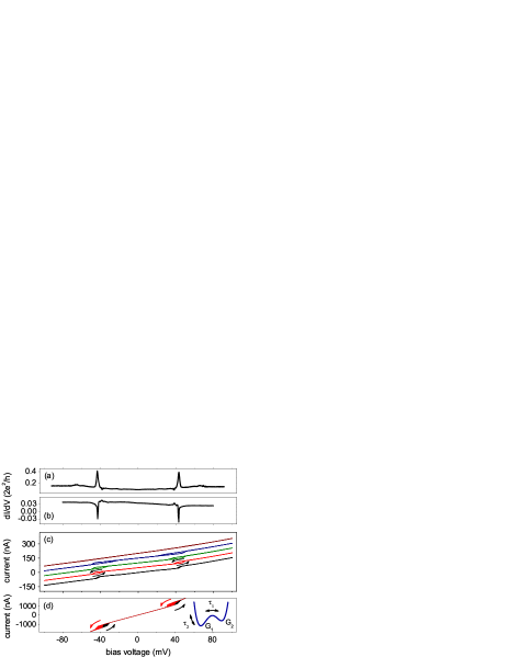
gupta ; thijssenprl ; halbritter ; temirov . In Fig.1,
we show two typical measurements for a contact. In one
case, two sharp peaks are observed (Fig.1a), whereas
in the other, two dips are seen (Fig.1b). Both curves
are symmetric with respect to voltage. Remarkably, the dip in
Fig.1b) is so deep that the differential conductance
around 43 mV becomes negative. Recently, Thijssen and
Halbritter et al. measured curves similar to Fig.
1a) and b) and put forward a two-level model
thijssenprl ; halbritter . The two levels (1, 2), most likely
representing different geometries of the contact, give
rise to two specific conductance values (, )
barnett . Hence, if transitions between level 1 and level 2
are induced at , the conductance changes discontinuously
from to an average of and (the weighing being
dependent on the degeneracy of the levels halbritter ). This
naturally results in a dip (if ) or peak (if )
in dI/dV, or analogously, in a step down or up in an I(V)-curve.
The latter is illustrated by the lowest I(V)-characteristic
presented in Fig. 1c). In both models proposed, a
double potential well is assumed to describe the two-level system
(schematized in Fig.1d), inset). However, there is
disagreement on the question how a transition between the levels
occurs. Halbritter et al. relate to the energy
difference between the two levels. Furthermore, they explain the
negative differential conductance by proposing that level 2 is
highly degenerate. In contrast, Thijssen et al. propose
that a transition is only possible if a molecular vibration is
excited with high enough energy to assist a jump
over the barrier. Hence, they conclude that , a statement for which they provide significant
experimental evidence. Regardless of the exact model, however, the
transition between states 1 and 2 is anticipated to be fast around
, with time scales ns, determined by tunnelling or
electron-phonon interaction. The results we present here, strongly
contradict this expectation. In Fig.1c), we show
I(V)-curves taken with various sweeping times. When slowly
ramping V, one obtains the lower curve discussed above. However,
when sweeping faster than 1 s per curve, a pronounced hysteresis
appears around . In other words, there is a macroscopic
time scale connected to the system’s return from the high
conductance state to the low one. Moreover, for even faster
voltage sweeps, Hz, the system does not have enough time
to relax back to state 1; it keeps the ’high’ conductance value
for all V. Not only does this not agree with the two-level models,
it also rules out the possibility that the steps in the I(V)’s are
due to resonant tunnelling. Hence, this intriguing
hysteresis forms the central item of this study.
To obtain stable molecular junctions, we employ mechanically
controllable break junctions agrait . Basically, a gold wire
is broken in cryogenic vacuum (at 5 K), and the electrode
tips are sharpened by a ”training” procedure PRL_G0loop .
Subsequently, a small volume of (99.999 pure) is
introduced and the junction is opened with 5 pm/s
vrouwe . Meanwhile, I(V)-curves are recorded by sweeping V
between and mV at Hz. After several
minutes, nonlinear I(V)-curves are observed with pronounced
conductance steps thijssenprl ; halbritter . During this
procedure, we do not observe a jump out of contact. In total, we
have used 6 break junctions on which 56 different
contacts were studied. To obtain geometrically different
junctions for one single device, we use the following procedure.
First, the junction is broken, resulting in a jump out of
contact. Then, the electrodes are pushed back into contact to
conductance values (where ). Finally, the
gentle pulling process is started again until a new
contact forms. To connect to previous work, we have first
investigated the I(V) curves of all these junctions at low voltage
scan rates. In Fig. 2a) we present a statistical
analysis of the on-set voltage . Interestingly, is
positioned around 40 meV, rather independent of the conductance of
the contact. Indeed, the zero bias conductances show a broad
variation between 0.003 and 0.3 . Since we did not observe a
jump out of contact while creating the junctions, this may point
to chain formation as reported in Ref. csonka5 . These authors find
conductance values in the same range as observed here. In Fig.
2b), we present a histogram of all values. The
average position is mV. This is in good agreement
with Thijssen et al, who found mV
thijssenprl . As explained above, they relate to a
phonon, which induces transitions between levels 1 and 2.
Experimentally, they provide two pieces of evidence.
First, they show that shifts down by a factor when is replaced by (deuterium). Second,
they show that upon pulling a junction, a step down in a
dI/dV-curve can evolve into a peak. Since a step in dI/dV is
related to the excitation of a phonon oren ; Thygesen , this confirms
their assertion. We have performed similar pulling experiments. In
some cases, peaks in dI/dV grew larger. In other cases, they would
virtually disappear, leaving a step as the dominant feature. This
confirms the result by Thijssen.

As we increase the scan velocity of our I(V)-scans, a hysteresis develops around (Fig.1c). Generally, we observe a smooth transition from one conductance state to the other. However, this is not always the case. The I(V)-scan in Fig.1d) for example, shows pronounced two levels fluctuations (TLFs) in combination with hysteresis. A comparison of Figs.1c) and d) leads to a number of important observations. First, the hysteresis is not an artifact of our electronics: TLFs much faster than the time scale of the hysteresis are easily observed. Second, the occurrence of TLFs confirms a two-level model. Halbritter et al. could not resolve the actual TLFs. Also in our case, most curves show an apparently smooth step around . This is due to the TLF frequency exceeding the bandwidth of the electronics ( kHz). Third, we see that the TLF-amplitude around is approximately equal to the difference between the ’low’ and ’high’ conductance states far away from . This indicates that for , the system is in state 2 most of the time. Hence, state 2 is either relatively stable or highly degenerate halbritter . Finally, we deduce from Fig. 1d) that despite continuous communication between both levels (through the TLFs), the hysteresis is still present. This suggests that the exact shape of the double potential well (at ) differs for the upward and downward voltage scans. We deduce that there are two time scales in our system: a time corresponding to fast switching between states (TLFs) and connected to changes in the effective potential landscape, resulting in hysteresis.
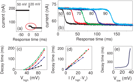
To gain more insight in , we have recorded response times using well-defined voltage pulses. An example is given in Fig.3a). First, V is set to a value , i.e. beyond the conductance step. The system’s conductance is ’high’. After 1 s, long enough to reach equilibrium, the voltage is instantly dropped to a value (in this case 20 mV). Interestingly, the current responds to this decrease within 20 , consistent with our bandwidth. However, the conductance does not. It is still ’high’ after 20 . Only after 10 ms, it starts to drop to a lower value. We define as the time in which the conductance drops halfway (dotted line in Fig.3b). Remarkably, we find larger for higher (see Fig.3b), which implies that depends on the history of the junction. We have systematically investigated vs. for 4 different contacts, as depicted in Fig.3c) 111Only voltage pulses 100 mV could be used since higher voltages led to irreversible changes in the molecular contact.. Clearly, increases more than linearly with , with an onset around 40 meV. In fact, if we plot as a function of we find a linear relation for all 4 samples (see Fig. 3d). Hence, there is a direct connection between and the power that was being dissipated before the voltage step, corrected for an onset value . From this interesting result, we deduce that heating effects (multiple phonon excitations) are at the basis of the hysteresis. The fact that mV serves as a threshold in all cases points to the pivotal role of a hydrogen phonon in this process thijssenprl . A second experiment that demonstrates this connection is shown in Fig. 3e). This measurement is similar to that in Fig. 3b). However, now is kept constant at 80 mV, whereas is systematically varied. We find that increases dramatically as approaches .
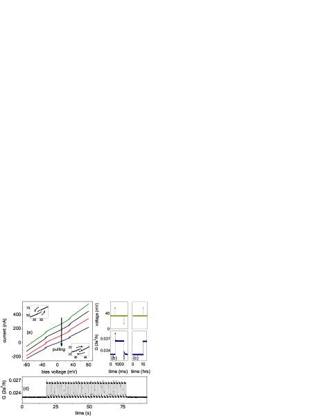
Remarkably, when slowly stretching the contact, a special type of hysteresis appears for the majority of the junctions. In general, a contact is stretched in steps of 10 pm while for each position an I(V) curve is measured (in 1 min). Fig.4a) shows 4 I(V)’s with 50 pm intervals. The upper curve is measured right after the contact is formed. With further stretching a hysteresis appears, which is most pronounced after 2 (lower curve). Interestingly, this type of hysteresis does not show any time dependence, contrasting the data above. Therefore, we can use it as a stable memory element. For this, we first apply an offset voltage . Subsequently, we switch conductance by applying positive (low G high G) or negative voltage pulses (v.v.). This is demonstrated in Fig.4b. The switch is remarkably stable in time. Even after 14 hours, no degradation is observed (see Fig. 4c). Furthermore, no deterioration is seen after multiple switching events (see Fig. 4d). We have performed over 5000 switching events, and saw no changes to the sample. Hence, we have created a switchable molecular device from the smallest molecule nature provides.
To discuss our observations, we first return to Fig.3. Here we concluded that heating, i.e. electron-phonon excitation, plays a pivotal role in the hysteresis. Furthermore, the molecular phonons are crucial in this process. We never observed heating effects on bare gold electrodes, which is consistent with the relatively low dissipation in our junctions (cf. Ref. kolesnychenko ). Recently, Galperin et al. and Chen theoretically studied the temperature of molecular junctions under a bias voltage galperin3 ; chenn . It is not trivial, however, to define a temperature for a single molecule. Galperin et al. approach this problem as follows. First, they assume that an external phonon bath is weakly coupled to the active mode of the molecule in the junction. Then, they calculate the ensuing heat flux between mode and bath. The bath temperature at which the heat flux vanishes is finally assigned to the molecular junction. For -junctions, a temperature increase K was predicted, exactly when the voltage reaches the phonon energy galperin3 ; chenn . From this, one might naively expect a hysteresis between upward and downward I(V)-scans. Going up in V, the molecule is ’cold’ and in state 1; coming down, the molecule is ’hot’, i.e. in a combination of states 1 and 2. However, it is highly unlikely that a single molecule will remain excited on time scales as large as ms. For the most likely relaxation mechanism, electron phonon coupling, typical time scales are ns, depending on the vibration mode pecchia . We propose that there is a larger phonon bath that preserves the energy for a relatively long time (cf. Galperin). A good candidate is formed by the large set of molecules that likely surround the actual molecule in the junction. At , these molecules will be excited by efficient phonon-phonon coupling from the junction outwards. After V is dropped below , it will take a relatively long time before this bath (and the molecule in the junction) is at the base temperature again. It may well be that heating of surrounding molecules actually induces a phase transition, although this is not essential to explain Figs. 1-3. In fact, we have only observed current steps at experimental temperatures below K. A phase transition has been proposed by Gupta and Temirov et al. to explain non-linear IV curves gupta ; temirov . Such a transition could indeed explain the time-independent hysteresis observed in Fig. 4. Upon a phase transition, the hydrogen phonon energy will most likely change. If it assumes a lower value than before (), the hydrogen molecule(s) will still be excited if the voltage drops below , provided that . This situation may be quasi-permanent, since the system is continuously excited. Only when V is decreased further, a transition back is expected. Our work may thus represent the first experimental case in which molecular heating is directly distinguished in a single junction galperin3 ; chenn .
In summary, we demonstrate that the presence of in a Au junction leads to two-level fluctuations, steps in I(V)-curves and hysteresis. Moreover, by carefully stretching the junctions, a reversible and stable molecular switch can be created. Interestingly, similar features have been reported for a large variety of molecular junctions, with molecules ranging from larger organic molecules to CO weiss ; blum ; emanuel ; thijssenprl ; gaudioso ; danilov . Since such switching effects are general phenomena in molecular electronics, there may be one basic mechanism behind them. In parallel, our work stresses the requirement to work in a hydrogen-free environment if one focuses on a different molecular system. Finally, we note that the steps in I(V)-curves (explained by a two-level model) may easily be confused with resonant tunnelling. To distinguish the two, fast I(V)-scanning is an efficient tool, since resonant tunnelling should not lead to hysteresis.
This work is financed by the Nederlandse Organisatie voor Wetenschappelijk onderzoek, NWO (Pionier grant), and the FOM program Atomic and Molecular nanophysics. We thank Frank Bakker, Simon Vrouwe, Siemon Bakker and Bernard Wolfs for technical support and Jan van Ruitenbeek and Roel Smit for discussions.
References
- (1) Feringa, B.L. (Ed.). Molecular Switches (Wiley-VCH, Weinheim, Germany, 2001).
- (2) D. Dulic et al., Phys. Rev. Lett. 91, 207402 (2003).
- (3) J. He et al., Nanotechnology 16, 695 (2005).
- (4) P. Liljeroth, J. Repp, and G. Meyer, Science 317, 1203-1206 (2007).
- (5) S.J. van der Molen et al., Nano Lett. 9, 76 (2009).
- (6) Z.J. Donhauser et al., Science 292, 2303 (2001).
- (7) A.S. Blum et al., Nature Mat. 4, 167 (2005).
- (8) E. Lörtscher et al., Small 2, 973 (2006).
- (9) S.Y. Quek et al., Nature Nanotech. 4, 230 (2009).
- (10) R.H.M. Smit et al., Nature 419, 906 (2002).
- (11) W.H.A. Thijssen et al., Phys. Rev. Lett. 97, 226806 (2006).
- (12) A. Halbritter et al., Phys. Rev. B 77, 075402 (2008).
- (13) J.A. Gupta et al., Phys. Rev. B 71, 115416 (2005).
- (14) R. Temirov et al., New journal of Phys. 10, 053012 (2008).
- (15) R.N. Barnett et al, Nano lett. 4, 1845 (2004)
- (16) N. Agraït, A.L. Yeyati and J.M. van Ruitenbeek, Physics Reports 377, 81 (2003).
- (17) M.L. Trouwborst et al., Phys. Rev. Lett. 100, 175502 (2008).
- (18) S.A.G. Vrouwe et al., Phys. Rev. B 71, 035313 (2005).
- (19) Sz. Csonka, A. Halbritter and G. Mihály, Phys. Rev. B 73, 075405 (2006).
- (20) O. Tal et al., Phys. Rev. Lett. 100 196804 (2008).
- (21) I.S. Kristensen et al, Phys. Rev. B 79, 235411 (2009).
- (22) O.Yu. Kolesnychenko et al., Appl. Phys. Lett. 79 2707 (2001).
- (23) M. Galperin, M.A. Ratner and A. Nitzan, J. Phys.: Condens. Matter 19 103201 (2007).
- (24) Yu-Chang Chen, Phys. Rev. B 78, 233310 (2008).
- (25) A. Pecchia, G. Romano, and A. Di Carlo, Phys. Rev. B 75, 035401 (2007).
- (26) J. Gaudioso, L.J. Lauhon and W. Ho, Phys. Rev. Lett. 85, 1918 (2000).
- (27) A.V. Danilov et al. Nano lett. 6, 2184 (2006).