Resistive switching in nanogap systems on SiO2 substrate
Abstract
Voltage-controlled resistive switching is demonstrated in various gap systems on SiO2 substrate. The nanosized gaps are made by different means using different materials including metal, semiconductor, and metallic nonmetal. The switching site is further reduced by using multi-walled carbon nanotubes and single-walled carbon nanotubes. The switching in all the gap systems shares the same characteristics. This independence of switching on the material compositions of the electrodes, accompanied by observable damage to the SiO2 substrate at the gap region, bespeaks the intrinsic switching from post-breakdown SiO2. It calls for caution when studying resistive switching in nanosystems on oxide substrates, since oxide breakdown extrinsic to the nanosystem can mimic resistive switching. Meanwhile, the high ON/OFF ratio (105), fast switching time (2 s, test limit), durable cycles demonstrated show promising memory properties. The intermediate states observed reveal the filamentary conduction nature.
Resistive switching in various materials such as metal oxidesszot ; yang , chalcogenideshirose and organic materialsouyang ; scot ; weitz has been intensively studied as candidates for future nonvolatile memorieswaser . Recently, it also extends to new quasi-one dimensional (1D) and 2D materials such as encapsulated nanowirescui , multi-walled carbon nanotubes (MWNTs)desh , and graphene sheetsst . In these nanostructures, the constriction in one dimension but less in the other(s) facilitates the observation of the switching events. The direct observations of nanosized gap or void structures in these systems come to similar switching mechanisms attributing to the electric close-and-break motion of the material at the gap/void region. Less attention has been paid on the substrate material of SiO2 due to its good dielectric (insulating) property. Meanwhile, the amorphous form of SiOmorgan ; simmons ; dear ; dear2 ; thurs ; shatzkes or a defected SiOx surfaceyao can exhibit memory phenomena, in which structural defects induced by high local field is one of the proposed causesmorgan . For a gap system at nano size, it is expected that a high local field is built up during the switches between high-impedance (OFF) and low-impedance (ON) states. It therefore carries the significance to investigate the local field effect on the commonly used substrate material of SiO2. In the following context, we demonstrate resistive switching phenomena in various nanogap systems on SiO2 substrate, made by different materials and means. The similar switching characteristics in all the systems point to the most likely cause: SiO2 breakdown (BD) induced filaments, possibly through Si-Si wire formation.
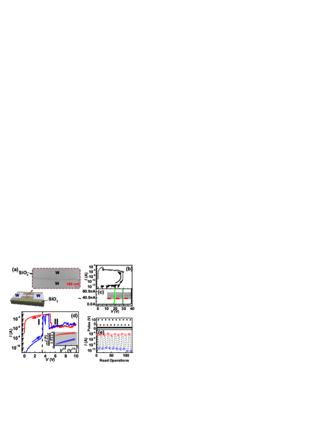
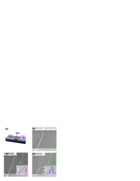
Shown in Fig. 1a, an initial gap system is a pair of tungsten (W) electrodes separated by 50 nanometers (nm) on a thermal-oxidized Si surface (the SiO2 thickness is 200 nm, and same thickness is used for all the following devices), defined by standard electron beam lithography (EBL) and lift-off process. Electrical characterizations were performed using an Agilent 4155C semiconductor parameter analyzer in vacuum environment ( 10-2 mTorr). Bias voltage was applied between the two electrodes by sweeping from 0 V to 30 V and then back to 0 V (see Fig. 1b). The device shows no conduction during the initial forward sweep from 0 V to 25 V (e.g., the current is at the noise level of the instrumentation of 10-12 A). Substantial conduction begins at 25 V with a sudden current rise at 30 V, indicating a SiO2 breakdown (BD). An irreversible resistance change takes place in the post-BD device, indicated by the increased current level during the subsequent backward sweep from 30 V to 6 V. The sudden current (or conductance) rise at 6 V in this backward sweep indicates the initiation of hysteretic current-voltage curves (I-Vs) essential for memory switching. Fig. 1d shows the two characteristic I-Vs of the post-BD device: In a forward sweep (0 V 10 V, blue curve), beginning with an OFF statestar , the device jumps to an ON state at 3.5 V and goes back to OFF at 5 V; in the backward sweep (10 V 0 V, red curve), it jumps from an OFF state to an ON state at 5 V and keeps the ON state below 5 V. Consequently, a current hysteresis is produced in the bias range below 3.5 V (region ”I” in Fig. 1d). The underlying information about the two I-Vs is that a fast voltage drop edge above 3.5 V (region ”II” in Fig. 1d) can set the conductance of the device into a value corresponding to that set voltagemorgan . For example, a +4 V pulse ”writes” the device into an ON state, while a +10 V pulse ”erases” the device to an OFF state. The set states can be read out in the lower bias region I without being destroyed, featuring the nonvolatile memory property. Fig. 1e shows the corresponding memory cycles by pulses as narrow as 2 s (our instrumentation limit) in the device, with an ON/OFF ratio approaching 105.
The SiO2 BD induced conduction is supported by the linear dependence of BD threshold voltage on the electrode-electrode spacing. Gap spacings of 30, 50, and 70 nm result in BD threshold values of 18 V, 29 V, and 39 V, respectively (see Fig. 1c). The corresponding averaged electric field is 6 MV/cm, which falls into the typical BD values of SiO2find (surface region is also expected to induce BD more easily than bulk given the less likeliness of defect free). The sudden current increase during the first sweep is accompanied by observable SiO2 substrate damage in the gap region. Subsequent forward or backward sweeps, usually undergo gradual current increases and fluctuations having the characteristics more and more alike those of the forward or backward I-Vs depicted in Fig. 1d. This electroforming precess, resembles that observed in vertical M/SiO/M (”M” denotes conducting electrodes) switching systemsmorgan , in which the amorphous form of SiO is the conducting and switching medium. The non-ohmic I-Vs, both for ON and OFF states, are dominated by Poole-Frenkel conduction having the characteristic of (see Inset in Fig. 1d). The calculatedcal Poole-Frenkel field-lowering coefficient () from the OFF state is very close to the theoretical one of and other experimental values in SiOxgould .
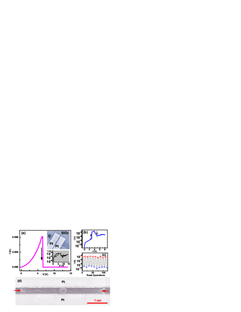
The electric field assisted BD in conducting materialsst ; naitoh ; tour offers another means for gap generation. A lift-off process was used to define an amorphous carbon (-C) stripe (50 nm thick, by sputtering from a carbon graphite target) on SiO2 substrate. Two platinum (Pt) electrodes, with a comparatively large spacing (0.4 m), were then defined (see top Inset in Fig. 2a). Bias voltage was applied between the two electrodes. The sudden current drop at 6.5 V (see Fig. 2a) indicates a BD in the -C stripe. Corresponding scanning electron microscope (SEM) image reveals a cracked region perpendicular to the current direction in the -C stripe (see Fig. 2d). The reduced conduction right after the -C BD (see the subsequent backward sweep in bottom Inset in Fig. 2a) has similar Poole-Frenkel feature, indicating the disruption of the -C layer and simultaneous BD in SiO2 in the gap region. The conductance jump at 7 V (bottom Inset in Fig. 2a) during this backward sweep, initiates the similar electroforming process as discussed above in the W-W gap (see Fig. 1b). The characteristic forward I-V (Fig. 2b) and switching (Fig. 2c) show similar features to those in the W-W gap (Fig. 1d-e) such as current levels, writing/erasing voltages, ON/OFF ratio, and switching time. While the threshold BD voltage in -C tends to be proportional to the electrode-electrode spacing, the writing/erasing voltages for switching tend to be independent of it, consistent with the local switching nature within the gap region (consider that the collective resistance of contacts and -C layer is considerably smaller than that of the gap region, the bias voltage largely drops across the gap).
Compared to the EBL defined W-W gap, the -C BD induced gap reduces the initial BD and electroforming voltage of SiO2 in the gap region, since the narrowest part is expected to be smaller than, e.g., 30 nm. On the other hand, it also offers an better way to investigate the details of the gap region by removing the -C layer without destruction to the SiO2 substrate. Ultra-violet ozone exposure (4 hours) was used to remove the -C in the same switching device. SEM image shows substantial damage to the SiO2 part corresponding to the gap region (compare Fig. 2d and e). Further control tests were performed in devices with same -C thicknesses and electrode spacings to investigate how the damage to SiO2 forms. In one group, we produced BD in the -C layer by one single sweep to a voltage above the -C BD threshold value, while in the other we performed multiple sweeps up to a voltage slightly below the -C BD threshold value (thus no gap generation). After the -C was removed, observable damage to the SiO2 substrate at the gap region in the first group was found, compared to no damage to the SiO2 substrate in the second group. The results reveal that: 1) gap generation in the above -C layer simultaneously induces SiO2 BD within the gap region, which is consistent with the reduced conduction (through post-BD SiO2) having the Poole-Frenkel feature right after the -C BD discussed above; 2) the damage to SiO2 is mainly through local electric-field induced BD, as opposed to local heating, since a great reduction in current local heating is expected after the disruption of -C layer in the gap region due to the sudden current drop. We also found that electroformed and switching devices tend to have more apparent damage in the SiO2 substrate than the ones having initial -C BD. These results indicate the role of SiO2 in switching in the gap region.
The post-BD SiO2 switching nature is further emphasized by using a different material as the gap generation medium. Electrical BD in a titanium nitride (TiN) stripe on SiO2 substrate leads to similar gap structure and switching (see supplementary material Fig. 7 at the end of the article). Compared to that in -C stripe, the gap in a TiN stripe is usually located at the TiN-electrode interface, instead of in between the electrodes. The possible reason is that the Schottky barrier at the TiN-electrode interface (since TiN is semiconducting) enhances the local field and facilitates the TiN BD there, as opposed to a good C-Pt electric contact in the -C stripe, where C BD is likely to happen at the least heat-dissipation region far away from both electrodes.

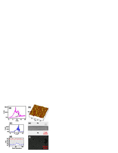
Gap by electric-field BD is less likely to form in metal stripes because the high current density usually melts the metal before a BD and the surface tension of liquid metal tends to form droplets, preventing a narrow and well aligned gap. However, thin metal film tends to form discreet islandsmetalislands , and nano gaps may form naturally between individual islands. For this purpose, aluminum (Al) thin film (10 nm thick) was deposited by sputtering on SiO2 between two Pt electrodes. The surface morphology of the deposited Al studied by atomic force microscope (AFM) shows discontinuous grained feature (Fig. 3b). Voltage sweep was applied between the two electrodes for the as-made device. Unlike that in -C or TiN stripes, the initial forward sweep (0 V 20 V) here shows much lower conductance and no sudden current drop (see Fig. 3a). This further indicates the discontinuity of the Al film. The subsequent backward sweep (20 V 0 V), with similar conductance jump, indicates the initiation of hysteretic behavior. The SEM image of the electroformed device shows grained Al surface between the electrodes (Fig. 3f) with no such apparent gap (Fig. 3e) as that produced by BD in -C or TiN stripes, which is consistent with the I-V feature of the initial sweep discussed and in support of the idea of switching in as-formed island-island gaps. Although the actual switching site is unknown due to numerous indistinguishable gaps between islands, it is expected that the relatively high resistance of Al film reduces both the current and effective voltage drop across the switching site. Therefore, the switching device has lower ON current (Fig. 3d) and higher writing/erasing voltages (Fig. 3c).
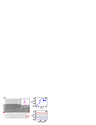
From the device part, one interesting question is how small the device can go. On the other hand, a small and constricted switching size may offer clearer view of the switching event, while it is relatively difficult to distinguish the actual switching site in a wide stripe, e.g., whether the switching happens uniformly along the entire gap region or locally. The electrical BD in MWNTschiu ; huang provides a potential means for further reduction in gap size. For this purpose, a MWNT with diameter 60 nm was patterned between two Pt electrodes (see Fig. 4a for illustration). Fig. 4b shows the SEM image of the pristine device. Electrical BD begins at a voltage 5 V indicated by a sudden current drop (see bottom Inset in Fig. 4c). The corresponding SEM image right after this BD shows a broken gap region (see Fig. 4c and top Inset). The subsequent sweeps electroform the device, showing the characteristic switching I-V (bottom Inset in Fig. 4d) similar to those observed in all the above devices. The SEM image of the electroformed device shows clear damage to the SiO2 at the gap region, extending outside (see Fig. 4d and top Inset). It is necessary to point out that switching in electrical BD MWNTs was reported beforedesh . The ON and OFF states were achieved by close-and-break motion of the carbon nanotube shells from the two broken ends, and were stable up to only several cyclesdesh . The switching here is attributed to the post-BD SiO2 at the gap region and can be stable against cycling (see Fig. 5c). The non-mechanical switching is also supported by the high yield in our devices (e.g. 10 out 10 MWNTs tested show similar switching), regardless of the actual details of the broken ends. This is in contradictory to mechanical switching as we expect both the broken gap size and morphology of broken ends would affect the switching.
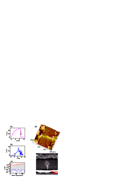
Single-walled carbon nanotubes (SWNTs) provide the candidates for ultra-small constrictions. Electrical BD in metallic SWNTs was reported and used as a means for semiconducting SWNTs sortingavouris . Metallic SWNT with a diameter 2 nm was patterned between two Ti/Pt electrodes. Electrical BD takes place at 8.5 V (see Fig. 5a). Fig. 5b-c show the characteristic I-V and switching after BD and electroforming. The AFM image of the electroformed device shows broken region in SWNT (Fig. 5d). The corresponding SEM image in Fig. 5e shows a dark dot at the gap region, indicating hole-like damage to the SiO2 substrate, which is also inferred from the AFM image. The comparatively small ON current (see Fig. 5c) in the SWNT device is mainly attributed to the contact resistance between the broken nanotube ends and the post-BD SiO2 in the gap region, as a good electric contact to metallic SWNTs with diameter below 2 nm usually requires specific metalsdai2 . This contact resistance also reduces the effective voltage drop across the gap, resulting in higher writing/erasing voltages (see Fig. 5b).
All the above devices share the similarities once operational. These include similar writing/erasing voltages and currents (the reduced ON currents and increased writing/erasing voltages in Al-island and SWNT devices are due to high film or contact resistances), switching time, and noise distributions. The comparatively large current fluctuation in the erasing bias region observed in all the devices is another characteristic of SiOx conductionmorgan . The largely independence of switching on the (effective) electrode materials ranging from metal (W, Al), metallic nonmetal (C), semiconductor (TiN), to carbon nanotubes, along with the electroforming processes and observable damage to the SiO2 substrate in the gap regions, bespeaks the intrinsic post-BD SiO2 switching nature. This is confirmed by making similar stripes and nanotube structures on Si3N4 substrate, in which switching was not observed after the gap generation (severe substrate damage is usually observed in the gap region by an attempt of electroforming). Another common feature observed in all the above devices is the various intermediate conduction states. As shown in Fig. 6a, for an initially established characteristic forward (0 7 V) I-V (green curve), an OFF state with a current level of 10-6 A can be set by a +7 V pulse (see cycles in the left column in Fig. 6b). By sweeping to a higher voltage above 7 V (black crossed curve), a lower conduction state appears, signatured by a sudden current drop at 7.5 V (see black arrow). In the subsequent sweep, a new I-V featuring a lower OFF state establishes (see blue curve), and the same +7 V pulse now sets the OFF state to a current level of 10-8 A (see cycles in the middle column in Fig. 6b). The OFF current can be further reduced by sweeping to an even higher voltage (see magenta crossed curve) during which a second conduction reduction appears at 12 V (magenta arrow). This leads to a third I-V (cyan curve) with an OFF current level of 10-10 A that can be set by the same erasing pulse of +7 V (see cycles in the right column in Fig. 6b). Multiple intermediate conduction states is an indication of filamentary conduction in oxideskim , in which different states can be viewed as formation/termination of new/existent percolation pathskim ; chen . To an extent, the current fluctuations in the erasing region (see cyan curve in Fig. 6a) can be viewed as various meta-stable states or excitons, e.g., same erasing voltages can produce different OFF currents if they encounter current fluctuations of different magnitudes. This is well reflected in a 103 cycles, in which the OFF states undergo various conductances (see Fig. 6c). We attribute this to be the main cause of instability in the current device performance.
In summary, we have demonstrated reproducible memory switching in various nanogap systems on SiO2 substrates. The lack of dependence of the switching behaviors on electrode materials points to a common mechanism, post-BD SiO2 switching in the gap region. It is therefore important to exercise caution when building resistive switching nanosystems on SiO2 substrate. Effects should be taken to distinguish the switching cause. The high ON/OFF ratio, fast switching time, and durable cycles demonstrated here show interesting memory properties. In particular, the small switching site demonstrated in a SWCNT shows the feasibility of high-density SiO2-based memory arrays if a vertical embodiment could be realized. The observed intermediate states reveal the filamentary conduction nature in post-BD SiO2 switching which is likely Si-Si wire formation, although a further investigation of the individual filamentary path is needed. The post-BD SiO2 conduction suggests another possible mechanistic scenario for the switching that was observed in our graphitic nanocablestour .
References
- (1)
- (2) K. Szot, W. Speier, G. Bihlmayer, and R. Waser, Nature Mater. 5, 312 (2006).
- (3) J. J. Yang, M. D. Pickett, X. Li, D. A. A. Ohlberg, D. R. Stewart, and R. S. Williams, Nature Nanotech. 3, 429 (2008).
- (4) Y. Hirose and H. Hirose, J. Appl. Phys., 47, 2767 (1976).
- (5) J. Y. Ouyang, C. W. Chu, C. R. Szmanda, L. P. Ma, and Y. Yang, Nature Mater. 3, 918 (2004).
- (6) R. C. Scott and L. D. Bozano, Adv. Mater. 19, 1452 (2007).
- (7) R. T. Weitz, A. Walter, R. Engl, R. Sezi, and C. Dehm, Nano Lett. 6, 2810 (2006).
- (8) R. Waser and M. Aono, Nature Mater. 6, 833 (2007).
- (9) meister S. Meister, D. T. Schoen, M. A. Topinka, A. M. Minor and Y. Cui, Nano Lett. 8, 4562 (2008).
- (10) V. V. Deshpande, H.-Y. Chiu, H. W. Ch. Postma, C. Miko, L. Forro, and M. Bockrath, Nano Lett. 6, 1092 (2006).
- (11) B. Standley, W. Bao, H. Zhang, J. Bruck, C. N. Lau and M. Bockrath, Nano Lett. 8 3345, (2008).
- (12) G. Dearnaley, A. M. Stoneham, and D. V. Morgan, Rep. Prog. Phys. 33, 1129 (1970).
- (13) J. G. Simmons and R. R. Verderber, Proc. Roy. Soc. A. 301, 77 (1967).
- (14) G. Dearnaley, D. V. Morgan, and A. M. Stoneham, J. Non-cryst. Solids 4, 593 (1970).
- (15) G. Dearnaley, Thin Solid Films 3, 161 (1969).
- (16) R. E. Thurstans, P. C. Wild, and D. P. Oxlety, Thin Solid Films 20, 281 (1974).
- (17) M. Shatzkes, M. Av-Ron, and R. M. Anderson, J. Appl. Phys. 45, 2065 (1974).
- (18) J. Yao, L. Zhong, D. Netelson, and J. M. Tour, Appl. Phys. Lett. 93, 253101 (2008).
- (19) A fast voltage drop edgemorgan is expected at the end of each forward sweep, which sets the device state. So the beginning conduction state for a forward sweep is determined by the previous forward sweep. Here the characteristic forward IV was obtained after at least another forward sweep prior to it in the same voltage range. So it begins with an OFF state. All the following characteristic forward IVs were obtained in this way, unless otherwise specified.
- (20) Y. Satoh, Y. Murakami, H. Furuya, and T. Shingyouji, Appl. Phys. Lett. 64, 303 (1994).
- (21) The Poole-Frenkel expressiongould is , where is the Boltzmann constant, the temperature, and the electric field. We used the room temperature and a gap width nm () for fitting.
- (22) R. D. Gould and M. G. Lopez, Thin Solid Films, 433, 315 (2003).
- (23) Y. Naitoh, Y. Morita, M. Horikawa, H. Suga, and T. Shimizu, Appl. Phys. Express, 1, 103001 (2008).
- (24) Y. Li, A. Sinitskii, and J. M. Tour, Nature Mater., 7, 966 (2008).
- (25) A. Wokaun, J. G. Bergman, J. P. Heritage, A. M. Glass, P. F. Liao, and D. H. Olson, Phys. Rev. B, 24, 849 (1981).
- (26) H. Y. Chiu, V. V. Deshpande, H. W. Postma, C. N. Lau, C. Miko, L. Forro, and M. Bockrath, Phys. Rev. Lett. 95, 226101 (2006).
- (27) J. Y. Huang, S. Chen, S. H. Jo, Z. Wang, D. X. Han , C. Chen, M. S. Dresselhuas, and Z. F. Ren, Phys. Rev. Lett., 94, 236802 (2005).
- (28) P. G. Collins, M. S. Arnold, and P. Avouris, Science, 292, 706 (2001).
- (29) W. Kim, A. Javey, R. Tu, J. Cao, Q. Wang, and H. Dai, Appl. Phys. Lett. 87, 173101 (2005).
- (30) D. C. Kim, S. Seo, S. E. Ahn, D.-S. Suh, M. J. Lee, B.-H. Park, I. K, Yoo, I. G. Baek, H.-J. Kim, E. K. Yim, J. E. Lee, S. O. Park, H. S. Kim, U-In Chung, J. T. Moon, and B. I. Ryu, Appl. Phys. Lett. 88, 202102 (2006).
- (31) T. P. Chen, M. S. Tse, and X. Zeng, Appl. Phys. Lett. 78, 492 (2001).