Optical study on the spin-density wave properties in single crystalline Na1-δFeAs
Abstract
We report an optical investigation on the in-plane charge dynamics for Na1-δFeAs single crystal. A clear optical evidence for the spin-density wave (SDW) gap is observed. As the structural/magnetic transitions are separated in the Na1-δFeAs case, we find the SDW gap opens in accordance with the magnetic transition. Comparing with the optical response of other FeAs-based parent compounds, both the gap value 2 and the energy scale for the gap-induced spectral weight redistribution are smaller in Na1-δFeAs. Our findings support the itinerant origin of the antiferromagnetic transition in the FeAs-based system.
pacs:
78.20.-e, 75.30.FvThe interplay between different instabilities, such as structural distortions, magnetic orderings, and superconductivity, is of central interest in condensed matter physics. The discovery of superconductivity in FeAs based layered materials Kamihara08 offers a new opportunity to study the intriguing interplay between those instabilities. The undoped FeAs-based compounds commonly display the structural and magnetic phase transitions, which, depending on materials, could occur either at the same temperature or separately.Cruz ; Rotter2 ; Chu The magnetic order has a collinear spin structure with a (, ) wavevector in the folded Brillioun zone (two Fe ions per unit cell). Upon electron or hole doping or application of pressure, both the magnetic order and the structural transition are suppressed, and superconductivity emerges.JZhao ; Rotter2 ; Torikachvili It is widely believed that the structural distortion is driven by the magnetic transition,Yildirim ; FangXu however, there have been much debate on whether the parent compounds belong to the local or itinerant category of antiferromagnets. One pool of theories invoke an itinerant electron approach to the systems in which the commensurate antiferromagnetic (AFM) order originates from a spin-density wave (SDW) instability due to the the nesting of the electron and hole Fermi surfaces which are separated by a (, ) wavevector.Dong ; Mazin ; Ran ; Tesanovic ; SinghReview The itinerant electrons and holes are removed by the gapping of the Fermi surface (FS) in the SDW ordered state. Alternatively, a Heisenberg magnetic exchange model is suggested to explain the AFM structure.Yildirim ; Si ; Ma ; FangXu ; Wu In this picture, the AFM order is a signature of local physics. On the other hand, Igor Mazin recently argued that neither the itinerant nor the local moment pictures are fully correct. The moments are largely local, driven by the Hund’s coupling rather than by the on-site Hubbard repulsion, while the ordering is driven mostly by the gain of the one-electron energies of all occupied states.Mazin3
The advantage for spectroscopic techniques is detecting the energy gap in the broken symmetry state. Previous optical investigations provide clear evidence for the formation of the SDW partial gap in the magnetic phase in polycrystalline ReFeAsO (Re=La, Ce, Nd, etc)Dong ; ChenPRLCe ; HuReview ; Boris and single crystalline AFe2As2 (A=Ba, Sr)Hu122 ; DWu which, therefore, support the itinerant picture that the energy gain for the AFM ground state is achieved by the opening of an SDW gap on the Fermi surface. Quantum oscillation experiment revealed three Fermi surfaces with area much smaller than those in the paramagnetic phase predicted by the local density approximation calculation,Sebastian thus agree with optical observation of a large reduction of effective carrier density in the SDW state. However, angle-resolved photoemission spectroscopy (ARPES) experiments did not yield consistent results.Kaminski ; Feng ; Hsieh ; GDLiu On the other hand, the iron chalcogen-based parent compound, Fe1+xTe, which also exhibits structural and magnetic phase transition near 65 K, shows no signature of gap opening for the magnetic ordered state from infrared spectroscopy measurement.Chen2 As neutron experiments revealed that the low-T magnetic phase has a bi-collinear spin structure with a (, 0) wavevector,Bao ; Li which is different from the (, ) wavevector that connects the electron and hole pockets, the absence of gap opening below TSDW is not surprising. Anyhow, further spectroscopic studies are required to find out whether the gap formation is a common feature for different types of Fe-based parent compounds. Another important question is whether the gap emerges after the structural distortion or below the magnetic transition. As the magnetic and structural transitions occur simultaneously in AFe2As2 (122-type), while no single crystal with sufficient size for optical measurement is obtained for ReFeAsO (1111-type), finding a new type of FeAs-based parent compound with well separated structural/magnetic transitions from which sizeable single crystals can be easily obtained is highly required.
Recently, high quality single crystals are synthesized for almost stoichiometric Na1-δFeAs, a 111-type FeAs-based parent compound. Two separated structural/magnetic transitions at 52 and 41 K, together with a superconducting transition at 23 K are found by transport measurements.ChenNaFeAs Here we report the in-plane optical properties for Na1-δFeAs single crystal. Clear optical evidence for the SDW gap is found, and the gap emerges in accordance with the magnetic transition. Moveover, the gap value 2 has a smaller energy scale than 122-type compounds with higher SDW transition temperatures. The ratio of 2/4.2 is close to the expectation of mean field theory for an itinerant SDW order. Like the 122 systems, a residual Drude term (free-carrier response) is seen in the SDW ordered phase, thus Na1-δFeAs is still metallic when the SDW gap develops. Then, metallic response and the SDW gap appear to be a common feature for the undoped FeAs-based materials.
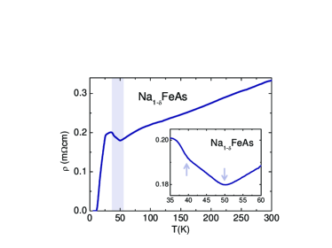
Single crystalline Na1-δFeAs samples were grown by the self-flux method.ChenNaFeAs The obtained crystals can be easily cleaved along ab-plane. The dc resistivity is obtained by the standard four-probe method on a sample cleaved from the same crystal used in the optical measurement. The result is shown in Fig.1. Two transitions near 40 and 50 K were assigned to separated structural and magnetic transitions,ChenNaFeAs which were confirmed by recent neutron diffraction measurement.LiNaFeAs Here the dc resistivity turns up after the structural distortion, and increases more rapidly with decreasing T in the SDW state. A superconducting transition is seen with an onset temperature of 25 K, and a zero resistivity is approached when T10 K. This was interpreted as due to the slight Na deficiency (less than 1%). Since no detectable specific heat anomaly around Tc was found, the superconducting volume fraction is rather small.ChenNaFeAs We expect that the optical data are dominated by the response of the parent phase.
The optical reflectance measurements were performed on a combination of Bruker IFS 66v/s and 113v spectrometers on newly cleaved surfaces (ab-plane) in the frequency range from 40 to 25000 cm-1. An in situ gold and aluminium overcoating technique was used to get the reflectivity R(). The real part of conductivity is obtained by the Kramers-Kronig transformation of R().
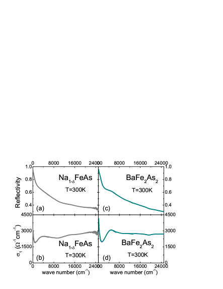
Figure 2 shows the room-temperature optical reflectivity and conductivity spectra over broad frequencies up to 25000 cm-1 . The overall spectral lineshapes are very similar to the AFe2As2 (A=Ba, Sr) single crystals. As a comparison, we have included the optical data on BaFe2As2 in the figure.Hu122 The reflectance drops almost linearly with frequency at low- region, then merges into the high values of a background contributed mostly from the interband transitions from the mid-infrared to visible regime. By fitting the conductivity spectrum with the Drude and Lorentz model in a way similar to what we did for 122-type crystals,Hu122 we get the plasma frequency 10200 cm-1 and scattering rate 650 cm-1 for Na1-δFeAs. Both are comparable to the parameters found for the 122-type materials.Hu122 ; DWu This indicates that we are measuring the charge dynamics of Fe2As2 layers.
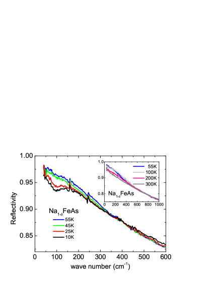
Figure 3 shows the optical reflectivity R( for Na1-δFeAs below 600 cm-1 . Two phonons around 160 and 244 cm-1 can be found. R( at low T decreases gradually below 400 cm-1 , consists with the increasing of below 50 K. In the SDW state, a suppression in R() below 150 cm-1 is observed, indicating the opening of an SDW gap on the Fermi surface. Similar cases were found for the undoped 122-typeHu122 ; DWu ; Pfuner and 1111-typeHuReview ; Boris compounds. Here the suppression exists only for T=10 and 25 K, while no clear indication for the gap is seen at T=45 K when the sample just experiences a structural distortion but without any magnetic ordering. The inset plots the low frequency R() for T=55, 100, 200 and 300 K. Here R( shows a metallic response in the far-infrared region, that the reflectivity continues to grow with lowering T in the normal state, in agreement with the metallic response as seen in the dc resistivity.
The low- temperature-dependent real part of conductivity is shown in Fig. 4. Besides two sharp phonon modes around 160 and 244 cm-1 , for both T=45 and 55 K show a Drude response without any clear evidence for the gap-induced absorption peak. For T=10 and 25 K, a peak with a clear edge-like feature is formed around 120 cm-1 . Therefore, the energy gap emerges only in the antiferromagnetic state. Meanwhile, a remaining Drude component is seen below 80 cm-1 , indicating that the Fermi surface is only partially gapped and Na1-δFeAs is still metallic in the SDW state. In our earlier study on AFe2As2 (A=Ba, Sr) single crystals, we know that the residual Drude component in the SDW state has a much smaller spectral weight and a narrower peak width, indicating the removal of both conducting carriers and the scattering channel.Hu122 Here, essentially we see the same structural feature. However, because of the limited frequency range below the energy gap, a quantitative estimation for the loss of carrier density and scattering rate could not be accurately determined.
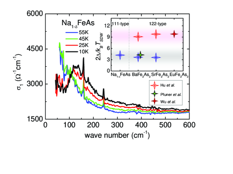
The optical conductivity shows different gap characters for the superconducting and the density wave states due to their respective coherence factors.Gruner ; Tinkham For the SDW ground state with an isotropic gap, a non-symmetric peak with clear edge-like feature emerges at 2 in the optical conductivity, so that exceeds the normal state conductivity at the gap onset,Gruner above which the loss in free-carrier (Drude) spectral weight is gradually compensated by the gap-induced absorption peak. For a multi-band system, gap anisotropy will weaken the edge-like feature at 2. Here we use the peak position (the conductivity maximum) to estimate the SDW gap. For Na1-δFeAs, the conductivity peak at 10 K is around 120 cm-1 , i.e., 215 meV. Such a gap is obviously smaller than that in AFe2As2 and ReFeAsO.Hu122 ; HuReview ; DWu ; Boris ; Pfuner
In undoped 122-type compounds AFe2As2, (A=Sr, Ba, Eu), a double-gap character is found with the 2/ 9 and 4, respectively. For Na1-δFeAs, only one energy gap feature is observed in the measurement frequency range with 2/ 4.2. From the spectral lineshape, this gap feature should correspond to the higher energy gap feature in undoped 122 compounds. It is not clear whether a second feature at lower energy scale exists beyond the lowest measurement energy. Thus, although qualitatively the energy gaps are smaller for undoped compounds with lower SDW transition temperatures, there is no scaling relation between different compounds with different . In the inset of Fig. 4 we show 2/ obtained by optical data on 111(Na1-δFeAs) and 122 (AFe2As2, A=Sr,Ba,Eu)Hu122 ; Pfuner ; DWu type parent compounds. Here the gap 2 for different FeAs systems are all defined by the peak positions in for consistency.
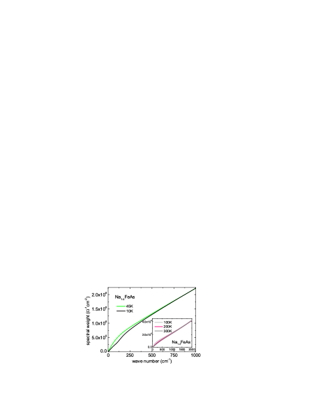
Besides the gap value, the energy scale affected by the SDW gap is also smaller for Na1-δFeAs in comparison with other FeAs-based parent compounds with higher TSDWs. Figure 5 plots the spectral weight at 10 and 45 K for Na1-δFeAs. The inset shows the spectral weight at T=100, 200 and 300 K. Note Na1-δFeAs is metallic in the normal state (Fig.1), so the spectral weight piles up at low frequencies with decreasing T, which is due to an increasing dc conductivity () thus a growing Drude peak in . Above 1700 cm-1 , the spectral weight for all temperatures merge together. In the SDW state, the spectral weight is smaller for 10 K than that of 45 K, indicating a loss in the Drude weight at 10 K, that part of the free carriers are removed from EF due to the SDW gap. The spectral weight loss in low frequencies is compensated when approaches 750 cm-1 . Such an energy scale is smaller than that of AFe2As2 (e.g. 2000 cm-1 for BaFe2As2 where TSDW140 K).Hu122
Our study clearly indicates that the metallic response and the opening of an energy gap in the magnetic ordered state are ubiquitous behaviors for all FeAs-based undoped compounds. In addition, the gap magnitude correlates with TSDW. Associated with the gapping of the Fermi surface, a large part of the Drude component is removed (indicating a reduction of the FS area) and the scattering channel is also reduced. All favor an itinerant origin of the SDW order. We noticed that some ARPES studiesFeng ; GDLiu on BaFe2As2 did not reveal any gap in the SDW state, therefore failed to see a dramatic reduction of Fermi surface areas. As the optics probes the bulk properties, while the ARPES is mainly a surface probe, it remains to clarify if there is a surface reconstruction which would affect the results. Considering the multi-band/orbital character for FeAs-based compounds, the entire band structure might be reconstructed when parts of them were modified by FS nesting instability. In this sense, our optical data do not conflict with the band reconstruction picture.
Finally, we comment on the upturn behavior of the dc resistivity below the structural/magnetic phase transition. Note turns up for Na1-δFeAs but drops more steeply with decreasing T for AFe2As2 and ReFeAsO. From the semi-classic Boltzmann transport theory, the resistivity is determined by the complex function of Fermi velocity, the scattering rate, and their weighted integral over the whole FS.Dressel In the case of electron gas, it could be simplified to the Drude form for which the resistivity is determined by carrier density and scattering rate. So apparently, whether shows an upturn or a fast drop depends on the subtle balance of those quantities which experience substantial changes across the transition.
To summarize, we studied the in-plane optical properties for Na1-δFeAs, a FeAs-based parent compound with separated structural and magnetic transitions. It shares similar optical response over broad frequencies with other FeAs-based systems. A clear energy gap in is observed below the magnetic phase transition, accompanied by a spectral weight transfer from the free-carrier Drude term to above this gap energy. Both the gap 2 and the energy scale associated with the spectral weight redistribution are smaller in comparison with other undoped FeAs-based compounds with higher TSDW. The results favor an itinerant origin for the SDW transition.
This work is supported by the NSFC, CAS, and the 973 project of the MOST of China.
References
- (1) Y. Kamihara, T. Watanabe, M. Hirano, and H. Hosono, J. Am. Chem. Soc. 130, 3296 (2008).
- (2) Clarina de la Cruz, Q. Huang, J. W. Lynn, Jiying Li, W. Ratcliff II, J. L. Zarestky, H. A. Mook, G. F. Chen, J. L. Luo, N. L. Wang, and Pengcheng Dai, Nature 453, 899 (2008).
- (3) M. Rotter, M. Tegel, D. Johrendt, Phys. Rev. Lett. 101, 107006 (2008).
- (4) J.H. Chu, J.G. Analytis, C. Kucharczyk, and I.R. Fisher, Phys. Rev. B 79 014506 (2009).
- (5) Jun Zhao, Q. Huang, Clarina de la Cruz, Shiliang Li, J. W. Lynn, Y. Chen, M. A. Green, G. F. Chen, G. Li, Z. Li, J. L. Luo, N. L. Wang, Pengcheng Dai, Nature Materials 7, 953 (2008).
- (6) M. S. Torikachvili, S. L. Bud’ko, N. Ni, P. C. Canfield, Phys. Rev. Lett. 101, 057006 (2008).
- (7) T. Yildirim, Phys. Rev. Lett. 101, 057010 (2008).
- (8) C. Fang, H. Yao, W.-F. Tsai, J. P. Hu, S. A. Kivelson, Phys. Rev. B 77, 224509 (2008); C. Xu, M. Mueller, S. Sachdev, Phys. Rev. B 78, 020501(R) (2008).
- (9) J. Dong, H. J. Zhang, G. Xu, Z. Li, G. Li, W. Z. Hu, D. Wu, G. F. Chen, X. Dai, J. L. Luo, Z. Fang, N. L. Wang, Europhys. Lett. 83, 27006 (2008).
- (10) I.I. Mazin, D.J. Singh, M.D. Johannes, M.H. Du, Phys. Rev. Lett. 101, 057003 (2008).
- (11) Ying Ran, Fa Wang, Hui Zhai, Ashvin Vishwanath, Dung-Hai Lee, Phys. Rev. B 79, 014505 (2009).
- (12) V. Cvetkovic and Z. Tesanovic, Europhysics Letters 85, 37002 (2009).
- (13) D. J. Singh, Physica C 469, 418 (2009) and references therein.
- (14) Q. Si and E. Abrahams, Phys. Rev. Lett. 101, 076401 (2008).
- (15) F. J. Ma, Z.Y. Lu, and T. Xiang, Phys. Rev. B 78, 224517 (2008).
- (16) J. Wu, P. Phillips and A. H. Castro Neto, Phys. Rev. Lett. 101, 126401 (2008).
- (17) M. D. Johannes and I. I. Mazin, Phys. Rev. B 79, 220510(R) (2009).
- (18) G. F. Chen, Z. Li, D. Wu, G. Li, W. Z. Hu, J. Dong, P. Zheng, J. L. Luo, and N. L. Wang, Phys. Rev. Lett. 100, 247002 (2008).
- (19) W. Z. Hu, Q. M. Zhang, and N. L. Wang, Physica C 469, 545 (2009).
- (20) A.V. Boris, N. N. Kovaleva, S. S. A. Seo, J. S. Kim, P. Popovich, Y. Matiks, R. K. Kremer, and B. Keimer, Phys. Rev. Lett. 102, 027001 (2009).
- (21) W. Z. Hu, J. Dong, G. Li, Z. Li, P. Zheng, G. F. Chen, J. L. Luo, and N. L. Wang, Phys. Rev. Lett. 101, 257005(2008).
- (22) D. Wu, N. Barišić, N. Drichko, S. Kaiser, A. Faridian, M. Dressel, S. Jiang, Z. Ren, L. J. Li, G. H. Cao, Z. A. Xu, H. S. Jeevan and P. Gegenwart, Phys. Rev. B 79, 155103 (2009).
- (23) Suchitra E. Sebastian, J. Gillett, N. Harrison, P. H. C. Lau, D. J. Singh, C. H. Mielke and G. G. Lonzarich, J. Phys.: Condens. Matter 20, 422203 (2008).
- (24) C. Liu, G. D. Samolyuk, Y. Lee, N. Ni, T. Kondo, A. F. Santander-Syro, S. L. Bud’ko, J. L. McChesney, E. Rotenberg, T. Valla, A. V. Fedorov, P. C. Canfield, B. N. Harmon, and A. Kaminski, Phys. Rev. Lett. 101, 177005 (2008).
- (25) L. X. Yang, Y. Zhang, H. W. Ou, J. F. Zhao, D. W. Shen, B. Zhou, J. Wei, F. Chen, M. Xu, C. He, Y. Chen, Z. D. Wang, X. F. Wang, T. Wu, G. Wu, X. H. Chen, M. Arita, K. Shimada, M. Taniguchi, Z. Y. Lu, T. Xiang, and D. L. Feng, Phys. Rev. Lett. 102, 107002 (2009).
- (26) D. Hsieh, Y. Xia, L. Wray, D. Qian, K. K. Gomes, A. Yazdani, G. F. Chen, J. L. Luo, N. L. Wang, and M. Z. Hasan, arXiv:0812.2289.
- (27) Guodong Liu, Haiyun Liu, Lin Zhao, Wentao Zhang, Xiaowen Jia, Jianqiao Meng, Xiaoli Dong, G. F. Chen, Guiling Wang, Yong Zhou, Yong Zhu, Xiaoyang Wang, Zuyan Xu, Chuangtian Chen, and X. J. Zhou, arXiv:0904.0677v2.
- (28) G. F. Chen, Z. G. Chen, J. Dong, W. Z. Hu, G. Li, X. D. Zhang, P. Zheng, J. L. Luo, and N. L. Wang, Phys. Rev. B 79, 140509(R) (2009).
- (29) W. Bao, Y. Qiu, Q. Huang, A. Green, P. Zajdel, M.R. Fitzsimmons, M. Zhernenkov, M. Fang, B. Qian, E.K. Vehstedt, J. Yang, H.M. Pham, L. Spinu, and Z.Q. Mao, arXiv:0809.2058.
- (30) Shiliang Li, Clarina de la Cruz, Q. Huang, Y. Chen, J. W. Lynn, Jiangping Hu, Yi-Lin Huang, Fong-chi Hsu, Kuo-Wei Yeh, Maw-Kuen Wu, and Pengcheng Dai, Phys. Rev. B 79, 054503 (2009).
- (31) G. F. Chen, W. Z. Hu, J. L. Luo, and N. L. Wang, Phys. Rev. Lett. 102, 227004 (2009).
- (32) Shiliang Li, Clarina de la Cruz, Q. Huang, G. F. Chen, T.-L. Xia, J. L. Lou, N. L. Wang, Pengcheng Dai, arXiv:0905.0525 (Phys. Rev. B, Rapid Commun.(in-press, 2009)).
- (33) F. Pfuner, J.G. Analytis, J.-H. Chu, I.R. Fisher, and L. Degiorgi, Eur. Phys. J B 67, 513 (2009).
- (34) G. Grüner, Density Waves in Solids (Addison-Weslsy, Reading, MA, 1994).
- (35) M. Tinkham, Introduction to Superconductivity(2nd Ed.), (McGraw-Hill, New York, 1996).
- (36) M. Dressel, and G. Grüner, Electrodynamics of Solids, Cambridge University Press (2002).