Band-like transport and trapping in TMTSF Single Crystal Transistors
Abstract
We perform a combined experimental and theoretical study of tetramethyltetraselenafulvalene (TMTSF) single-crystal field-effect transistors, whose electrical characteristics exhibit clear signatures of the intrinsic transport properties of the material. We introduce a simple, well-defined model based on physical parameters and we successfully reproduce quantitatively the device properties as a function of temperature and carrier density. The analysis allows its internal consistency to be checked, and enables the reliable extraction of the density and characteristic energy of shallow and deep traps in the material. Our findings indicate that shallow traps originate from electrostatic potential fluctuations generated by charges fixed in the deep traps.
Despite impressive progress in the use of organic semiconductors for the realization of practical circuits and devices, our fundamental understanding of these materials remains limited. In this context, the recent observation of an anisotropic carrier mobility increasing with lowering temperature in organic single-crystal field-effect transistors (FETs)Review establishes a breakthrough, because it opens the possibility to investigate intrinsic transport properties of molecular materials at finite and tunable carrier densitySundar04 ; Podzorov04 . Surprisingly, a systematic, in-depth analysis of the intrinsic transport phenomena observed in single-crystal FETs has not been attempted yet. In large part, this is due to the lack of a well-defined model enabling a quantitative study to be performed. In fact, past work on the intrinsic transport properties of organic semiconductors –based on time-of-flight measurements– has relied on the so-called trap-and-release modelKarl ; Horowitz , which, despite being helpfulCalhoun , cannot be applied to the systematic analysis of systems at finite carrier density. This poses a clear problem, because a quantitative analysis of the properties of organic semiconductors is essential to characterize devices and materials unambiguously, to perform comparative studies, and to reach a true microscopic understanding, which is essential for the efficient long-term development of practical applications.
We address this issue through a combined experimental and theoretical study of transport through tetramethyltetraselenafulvalene (TMTSF, C10H12Se4, see Fig. 1a) single-crystal FETs. We first show that these devices exhibit the characteristic signature of the intrinsic transport properties. We then introduce a simple model based on physically transparent quantities and assumptions, with which we analyze in detail the temperature and density dependence of the mobility, and the temperature dependence of the threshold voltage. Our analysis reproduces the observations systematically and quantitatively, it gives consistent results on different devices, it enables the reliable determination of the concentration and characteristic energy of traps, it allows the check of its internal consistency to be performed, and it points to the physical origin of the shallow traps. These results clearly indicate that the model represents an appropriate framework for the analysis through high-quality organic FETs.
So far, rubrene crystals have been the only ones to unambiguously show the expected signatures of intrinsic transport at finite carrier density in a FET configurationReview . We have explored crystals of different molecules, and here we discuss TMTSF transistorsChaikin , realized by laminating a single-crystal grown from vapor phase transport onto a polydimethylsiloxane (PDMS) support as shown in Fig. 1b,c (the fabrication procedure is identical to that described in Ref. Menard ). Immediately after fabrication, the devices were transferred into the vacuum chamber ( mbar) of a flow cryostat where all transport measurements were done. Most measurements were made using a HP 4156A parameter analyzer, in a four-terminal configuration (Fig. 1 (c)), to eliminate the effects of the contact resistance. We discuss data taken on three different FETs, representative of the approximately 10 devices studied.

Fig. 2(a) shows the source-drain current (ISD) measured at different temperatures, as a function of gate voltage (VG), and the inset measured on the same device as a function of at T=300 K, for different values of . The measurements exhibit the characteristic behavior of high-quality devices (e.g., absence of hysteresis, stability and reproducibility). The charge carrier mobility is extracted from the linear part of ISD-VG characteristics, using the relation (with separation between voltage probes, crystal width, Ci gate capacitance per unit area, and V voltage difference measured between the two voltage probes). At room temperature, cm2/Vs reproducibly (the same value is obtained from the characteristics in the saturation regime). From the curves we extract the full temperature dependence of the mobility, as well as the threshold voltage (by extrapolating the curves to zero current).
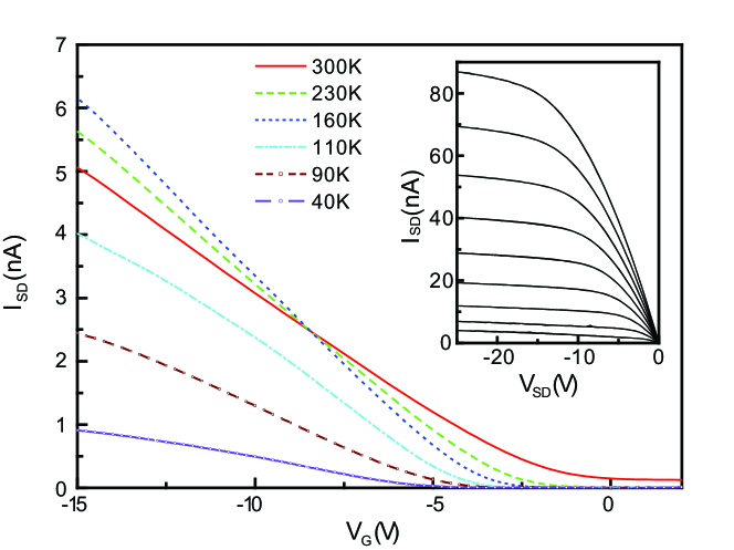
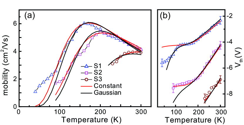
Fig. 3a and b show the mobility and threshold voltage as a function of temperature measured on three different samples. The mobility tends to increase, exhibiting an identical temperature dependence down to a sample-dependent temperature value, after which decreases with further lowering . The temperature interval where is ”metallic-like” reflects the intrinsic material properties, and the different extents of this interval in the three samples indicate that different amount of disorder is present. Interestingly, the decrease of the mobility at low is very slow. In our best sample, reaches a value above 6 cm2/Vs at K, and it is still close to 2 cm2/Vs at 50 K. The behavior of the threshold voltage is qualitatively similar in different devices –exhibiting a linear decrease with lowering at first, and a tendency to saturate at lower . The magnitude of depends on the sample, and it is systematically smaller in higher mobility devices (i.e., the experiments indicate that the temperature dependence of correlates with the values of ).
To analyze quantitatively the data we introduce a model based on the assumption that transport of holes in TMTSF occurs in a band (with density of states for energy ), and that disorder-induced trap states are present (for )(see also Merlo ). These consist of shallow traps (with density of states ) and deep traps located much deeper in energy (described by a density of states ). The mobility of carriers occupying states in the band is the intrinsic mobility in the material, and, following existing theories, is assumed to depend on temperature as Troisi ; Hannewald ; exponent . Carriers occupying trap states are assumed not to carry current.
In practice, we fix the shape of the density of states and calculate the position of the Fermi level (numerically) as a function of the total density of accumulated charge () through the relation:
| (1) | |||||
that defines . Having determined , it is straightforward to obtain the source-drain current in terms of the density of charge carriers occupying states in the band () as:
| (2) |
From Eq. 2 we extract all quantities that are measured in the experiments, by applying to the calculated curves the same procedures used for the measured ones. For instance, the mobility measured from the FET characteristics is simply given by (which corresponds to ). For our calculations we use, for the shallow traps, a constant density of states ( const, if , and otherwise), and a gaussian density of states (), and compare the results obtained imposing that the total number of shallow traps is the same for the two distributions. For the deep traps we use a ”square” distribution ( constant if and zero otherwise) to analyze the role of the trap depth () and of the distribution width (). The density of states in the band at the surface of the TMTSF crystal – cm-2 eV-1– is estimated by taking one state per molecule distributed in energy over the bandwidth of the valence band ( eV Silinsh ). The parameter (in the expression ) represents an intrinsic property of TMTSF crystals, and it is taken to be the same for all samples.
A strategy similar to the one adopted here –i.e., ”fixing” a density of states to analyze transport through FETs– is used to describe transport in FETs based on amorphous materialsBrutting . In that case, however, transport is due to carriers occupying localized states, whose mobility is strongly energy dependent, and material inhomogeneity requires percolation effects to be taken into accountMatters . This significantly increases the complexity of the analysis, as well as the unambiguous extraction of parameters in the model. These problems are absent in high-quality single-crystal FETs. Only at low temperatures, such that most carriers occupy trap states, the model starts to deviate from the experiments, mainly because our assumption that carriers in the shallow traps do not carry any current is too restrictive. For this reason, we limit our analysis to a temperature range where a significant fraction of carriers populate states in the band. In this temperature range (between approximately 100 and 300 K for the best device) we find that the behavior of the temperature dependence of the mobility measured at high carrier density curve depends only on the properties of the shallow traps (Fig. 3a), whereas the behavior of the is determined only by the deep traps. This considerably simplifies the analysis.

Best fits to the temperature dependence of the mobility are shown in Fig. 3(a), using both the gaussian and the constant distributions of shallow traps. With both distributions the agreement is satisfactory for the temperature range discussed aboveexponential . Table 1 summarizes the parameters extracted from the fits. Note that the energies and satisfy the relation to a 10% precision (or better) for all samples, which can be easily understood since the integral of the gaussian trap distribution between and gives 99% of the shallow trap states. Since different distributions lead to nearly identical temperature dependencies of the mobility, the precise energy distribution of the shallow traps cannot be extracted from the analysis. On the contrary, the total density of shallow traps and of their characteristic energy () are not sensitive to the details of the model, and the values extracted have therefore physical meaning.
The microscopic analysis of the threshold voltage is meaningful, because in our FETs the single-crystals are suspended on top of the gate, which eliminates extrinsic effects due to phenomena taking place in the gate insulator. We find that the curve is sensitive to both the energy and the width of the deep trap distribution. Specifically, very deep traps (whose energy is larger than roughly 0.5 eV) contribute to the threshold voltage, but do not cause a shift in the temperature range considered. In this same range, a sizable contribution to the threshold voltage shift originates from traps with energy between 100 and 400 meV, approximately, with the largest contribution coming from traps between 150-200 meV. This fact –that deep traps at different energies affect differently and its shift with temperature– makes it possible to extract information on the energy distribution of deep traps from the experimental curves. With the parameter values listed in Table 1, the model leads to an excellent quantitative agreement with the data (again, below approximately 100 K, where the majority of carriers occupies shallow traps, the results depend on the details of the shallow trap distribution). Note that the center of the deep trap distributions is approximately the same in the three devices. This is expected if deep traps originate from a well-defined chemical impurity hosted in the crystal. Indeed, the values of and of extracted from our analysis are in the same range energies and widths of other deep traps recently found in different molecular materialsdeeptraps .
| Sample1 | Sample2 | Sample3 | |
| NC(cm-2 eV-1) | 1.97*1014 | 8.5*1013 | 9.3*1012 |
| EC(meV) | 38.5 | 54.1 | 111 |
| Ng(cm-2 eV-1) | 3.04*1014 | 1.36*1014 | 1.42*1013 |
| Eg(meV) | 14.1 | 19.1 | 40.8 |
| (cm-2) | 7.6*1012 | 4.6*1012 | 1.03*1012 |
| ND(cm-2 eV-1) | 6*1010 | 1.08*1011 | 1.08*1011 |
| ED(meV) | 225 | 235 | 270 |
| ED(meV) | 95 | 95 | 130 |
| (meV) | 10.3 | 13.7 | 16.1 |
With the model reproducing successfully the experimental observations, it is important to critically ask whether the quantitative agreement is not simply due to the introduction of a sufficient number of free parameters. To show that this is not the case, we have analyzed the full dependence of the mobility on carrier density, at different temperature values. This comparison provides a stringent test of the validity of the model and of its consistency, because all parameters are fixed by the analysis discussed above, and no other free parameters can be introduced. Fig. 4a and b show that the curves calculated with the model are in excellent quantitative agreement with the data, as long as the temperature is such that enough charge carriers are present in the band. This result confirms the internal consistency of our analysis, and illustrates that the model does describe well the interplay between band-like transport and trapping as a function of carrier density.
Having established the internal consistency of our analysis, we address the origin of the observed correlation between the temperature dependence of mobility and of threshold voltage. Since the temperature dependence of the mobility is determined only by the shallow traps and that of the threshold voltage only by the deep traps, this correlation implies that a physical mechanism exists, that links the origin of the two kinds of traps. We propose that this mechanism is due to simple electrostatics. Individual charge carriers frozen in the deep traps generate random electrostatic potential fluctuations , and the resulting electrostatic potential landscape causes regions of lower energy in which a large density of charge carriers can be trapped. The characteristic energy scale associated to the potential fluctuations can be estimated as , where is the average distance between deep traps and is the average of the relative dielectric constant of the TMTSF crystal and of vacuum. By estimating the magnitude of from the total density of deep traps extracted from the fit of , we obtain the values of reported in Table 1, whose magnitude compares well with the characteristic energy scale of the shallow traps. This scenario explains why the density of states of shallow traps at is comparable to the density of states in the band itself. In fact, shallow traps consist of states in the band whose energy is lowered by the local, slowly varying electrostatic potential. It also explains why carriers in shallow traps contribute significantly to the conductivity (as we noticed earlier), since these carriers are not tightly bound to a defect and can move over rather large distances.
In conclusion, we have developed a well-defined framework to analyze the interplay between intrinsic band-like transport and trapping in organic single-crystal transistors and used it to describe the behavior of newly developed TMTSF FETs. The model permits to understand in detail the physical origin of the different aspects of the device characteristics, and to extract microscopic parameters reliably. This combination of experimental investigation on high-quality devices and systematic quantitative analysis is important to reach a true understanding of molecular semiconductors at finite density of charge carriers.
We are grateful to S. Fratini for discussions and comments, and we acknowledge financial support from NanoNed, the Swiss NCCR MaNEP, NEDO, and FCT.
References
- (1) R. W. I. de Boer, M. E. Gershenson , A. F. Morpurgo and V. Podzorov, Phys. Status Solidi (a) 201, 1302 (2004); M.E. Gershenson, V. Podzorov, and A.F. Morpurgo, Rev. Mod. Phys. 78, 973 (2006).
- (2) V. C. Sundar, et al., Science 303, 1644 (2004)
- (3) V. Podzorov et al., Phys. Rev. Lett. 93, 086602 (2004)
- (4) W. Warta and N. Karl, Phys. Rev. B 32, 1172 (1985)
- (5) G. Horowitz, M.E. Hajlaoui, and R. Hajlaoui, J. Appl. Phys. 87, 4456 (2000)
- (6) M.F. Calhoun, C. Hsieh, and V. Podzorov, Phys. Rev. Lett. 98, 096402 (2007)
- (7) M.S. Nam et al., Appl. Phys. Lett. 83, 4782 (2003)
- (8) E. Menard et al., Adv. Mat. 16, 2097 (2004)
- (9) J.A. Merlo et al., J. Am. Chem Soc. 127, 3997 (2005)
- (10) A. Troisi and G. Orlandi, Phys. Rev. Lett. 96, 086601 (2006)
- (11) K. Hannewald and P.A. Bobbert, Appl. Phys. Lett. 85, (2004)
- (12) Presently, our analysis cannot discriminate between small differences in the value of the exponent, which depend on details of the theoretical models.
- (13) E.A. Silinsh and V. Capek, ”Organic Molecular Crystals”, AIP (1994)
- (14) For a general overview see Chapter 12 of ”Physics of Organic Semiconductors”, Wiley 2005, and references therein.
- (15) M.C.J.M. Vissenberg and M. Matters, Phys. Rev. B 57, 12964 (1998)
- (16) We have obtained similar and consistent results also with an exponential distribution. With such a distribution, however, the threshold voltage below 100-150 K is suppressed much more rapidly than with the constant or gaussian distributions.
- (17) D.V. Lang et al., Phys. Rev. Lett. 93, 086802 (2004); O. Mitrofanov et al, Phys. Rev. Lett. 97, 166601 (2006); C. Krellner et al., Phys. Rev. B 75, 245115 (2007)