Current Driven tri-stable Resistance States in Magnetic Point Contacts
Abstract
Point contacts between normal and ferromagnetic metals are investigated using magneto-resistance and transport spectroscopy measurements combined with micromagnetic simulations. Pronounced hysteresis in the point-contact resistance versus both bias current and external magnetic field are observed. It is found that such hysteretic resistance can exhibit, in addition to bi-stable resistance states found in ordinary spin valves, tri-stable resistance states with a middle resistance level. We interpret these observation in terms of surface spin-valve and spin-vortex states, originating from a substantially modified spin structure at the ferromagnetic interface in contact core. We argue that these surface spin states, subject to a weakened exchange interaction, dominate the effects of spin transfer torques on the nanometer scale.
Spin Transfer Torques (STT) slon ; berger between the conduction electrons and the magnetic lattice in a ferromagnet can cause a rotation of the magnetization when the electron current density is sufficiently high and spin-polarized. The most common geometry for using this effect is a spin-valve with two closely spaced ferromagnetic layers, where one is magnetically hard and acts as the current polarizer, and the other is magnetically soft and can magnetically precess or switch from the action of the polarized current. It has recently been demonstrated that similar in origin magnetization excitations occur for single ferromagnetic films and interfaces polianski ; stiles ; Ji , where the STT is intra-layer and is mediated by impurity scattering yansonPRL . We have recently shown yansonNL using ultra thin Co films that STT driven switching can occur in atomically thin spin layers at nonmagnetic/ferromagnetic (N/F) interfaces, which form spin-valve like states with respect to the interior spins, within the same ferromagnetic film. Here we present experimental results indicating that such surface spin states can form stable spin vortices, and the current driven STT switching in the system can involve parallel, anti-parallel, and vortex spin states, yielding three stable resistance states of the ferromagnetic interface.
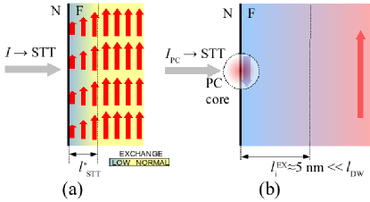
The STT literature to date ralph_stiles has essentially ignored the fact that the spin states at a ferromagnetic interface can have distinctly different properties from those of the interior spins. This fact should be of crucial importance since the STT effect is in nature a surface effect slon99 . In the ideal case, universally assumed to be valid in the STT studies, the fundamental characteristics of the magnetic interface - the exchange strength, magnetization magnitude, and anisotropy strength and direction – are assumed to be identical to those in the interior of the ferromagnet. In this case the interface and the interior spins respond as one system to a current driven STT, which is known to be concentrated in an atomically thin layer at the ferromagnetic surface slon99 . In the realistic case shown in the Fig. 1(a), the exchange, magnetization, and anisotropy can be significantly different at the interface from those in the bulk. For example, recent surface versus bulk magnetization measurements for Co and Fe gruyters ; jonker show different anisotropy and coercivity for the surface and interior spins. This should significantly modify the response of the N/F interface to a current driven STT, which we indeed observe yansonNL .
In this paper we study point contacts (PC’s) between Co films of different thickness and sharpened wires of normal metal (Ag, Cu). The films and PCs were prepared as described in yansonPRL ; yansonNL . Fig. 2 shows the data for one of our smallest PC’s, with the resistance of about 80 and the radius of the contact core estimated at 1.5 nm using the well-known Sharvin formula. The PC resistance shows pronounced hysteresis, which has two distinct stable states at zero bias and appears indistinguishable from the STT hysteresis frequently reported for three-layer spin-valves Albert .
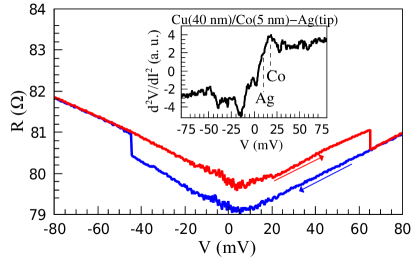
The data for our nanometer scale PCs, of the kind shown in Fig. 2, allow us to draw the following important conclusions. First, the presence of the Co 111The poorly resolved Ag phonon maximum in Fig. 2(inset) is due to a few times weaker electron-phonon interaction in Ag compared to that in Co (see, e. g., Naid ), and possibly due to a smaller partial-volume of the PC core occupied by Ag. phonon maximum indicates that the PC consists of the ferromagnetic metal of good crystalline quality. Secondly, the rather high resistance of this PC means that the size of the contact core is in fact smaller than the exchange length in Co (4–5 nm), and much smaller than any domain wall that can be created in the ferromagnet (domain wall length typically 5–10 times the exchange length Rave ). Fig. 1(b) illustrates these fundamental ferromagnetic length scales in comparison to our experimental results. In the case of our thinner 5 nm-Co film (Fig. 2) the thickness is approximately the same as the bulk exchange length in Co, so any volume-like domain walls along the current can be excluded. In the case of our thicker ferromagnetic films (100 nm thick Co, Fig. 3), possible domain walls would be far outside the PC core and thus make essentially no contribution to the measured resistance. Based on this principal comparisons we can rule out the interpretation of the resistance hysteresis as due to a bulk-like domain-wall magnetoresistance (MR) ChenStilesBiasExch , and conclude that the observed STT switching must be due to the spins in the surface layer of the ferromagnet, changing their orientation with respect to the interior spins yansonNL .
In order to make such surface versus bulk spin re-orientations possible either the exchange interaction or anisotropy, or both must be of different strength at the interface compared to the interior of the ferromagnet gruyters ; jonker . The data and the micromagnetic simulations below demonstrate these surface magnetism effects in the current and field driven MR of N/F interfaces.
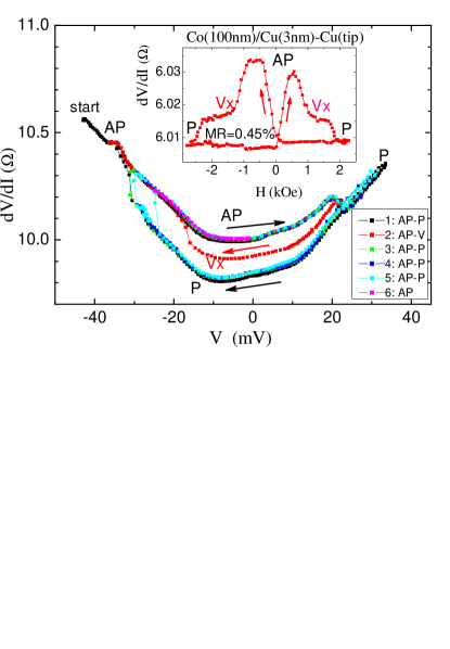
Fig. 3 shows resistance versus bias voltage data for a Co–Cu PC. Five out of six sweeps recorded follow the major hysteresis loop, designated as the P–to–AP switching loop. This current driven P–AP MR of approximately 1.8% is essentially the same as the field driven P–AP MR of 1.6% (not shown), which shows the high reproducibility of the micromagnetic states involved. One sweep (No. 2, red curve) shows a third resistance state, found at the mid-point between the P and AP resistances. This intermediate resistance position means that effectively only one half of the surface spins participating in the magneto-transport are in the AP state – the configuration expected for a spin vortex state. Indeed, if the spins at the interface, within the contact core, could form a stable vortex, the MR of the interface should have form shown in Fig. 3, with three approximately equidistant levels.
Of the PCs showing 3-level hysteresis, which is a 10% subset of the PC’s showing hysteretic , some contacts display a very characteristic field dependence of MR 222The correlation between the field and current induced magneto-resistance is normally taken as a confirmation of an STT effect (see e. g. Albert ). Obviously, a homogeneous external magnetic field does not favor spin vortex states, which makes them much less probable than the uniform spin states.. An example of this is shown in the inset to Fig. 3 for another Co–Cu contact. Sweeping the external field from the saturated P state of the PC through zero induces a switching in the softer underlying Co film with respect to the surface magnetic layer, 333According to gruyters :”For pure Co film the reversal of the bulk magnetization is preceded by a complete reversal of the surface magnetization”, however Fig. 2e from this paper displays that in the case of the less perfect Co film noticeable part of surface requires higher than for a bulk field for a complete reversal. In our case the surface layer under study is restricted within a nanoscale PC size, therefore it is pinned strongly compared to the bulk and needs higher field for reversal of magnetization. thereby placing the interface/bulk into the AP state. As the field is increased further, the intermediate-resistance state appears at 1–2 kOe, and is subsequently saturated in still higher fields. The shape of the curves has a striking similarity to the three-level hysteresis recently reported in yangVRTX (see their Figs. 2,3), where a spin-vortex state was intentionally created in one of the ferromagnetic layers (ring-shaped in fabrication) of a 100 nm scale spin-valve nanopillar. Similar to yangVRTX , we can transform our 2-level P–AP hysteresis loops into 3-level P–V–AP loops by suitably limiting the field sweep amplitude. The same three-level hysteresis is found also in zero field sweeps for this contact, with the same magnitude (0.5%) of the P–AP MR (not shown). These vortex-no vortex transformations are fully reversible. The high similarity between our three-fold hysteresis data and the vortex-based spin-valves of yangVRTX provides further support for our interpretation of the observed switching behavior in nano-sized PCs in terms of surface spin-valve and spin-vortex states, which can be reoriented by current-induced STT or external magnetic field.
It is informative to note that non-uniform magnetization states, such as magnetic vortices, were suggested to explain spin dynamics in larger, 100 nm scale point contacts Puffal ; Mistral , where the vortex core would oscillate at relatively low-frequency (500MHz), driven by a spin-polarized current. In Balk09 we observed a peak in for 10 nm scale Co-Cu point contacts stimulated by external RF fields, which we interpreted as excitations of resonant magnetization precession. The typical resonant frequencies observed in our experiments were in the range 1-10 GHz, which is relatively low compared to the FMR frequency expected for a uniformly magnetized film or particle in a field of about 1 T (10 GHz). Therefore, we cannot exclude that the spin-torque dynamics effects we observed previously originate from spin dynamics in non-uniformly magnetized nano-objects, such as spin vortices, where the characteristic frequencies are typically lower than those for uniform spin systems.
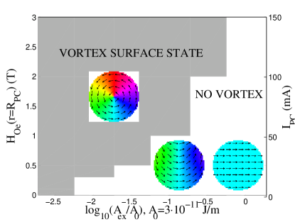
The fact that the nanopillars of yangVRTX and our PCs differ in size by an order of magnitude is important. In our case, in order to produce the relatively large MR observed, the spin-vortex must be of the similar small size as the contact core. Our numerical micromagnetic analysis metlov shows that such 10 nm scale spin-vortex states can only be produced if the exchange interaction strength is assumed to be significantly lower at the interface compared to that in the bulk. To illustrate this, we simulate stable spin configurations in a 1 nm thin disk of radius 10 nm. The disk is discretized into a 3D mesh of cubic cells having the magnetization and anisotropy typical for Co, and varying exchange stiffness from to the bulk value of J/m. We assume that the bias current is uniformly distributed across the PC, and the Oersted field it produces within the contact core to be , where . The resulting vortex phase diagram obtained by the micromagnetic minimization oommf is shown in Fig. 4. The results of this qualitative simulation are quite intuitive - no nano-sized vortex states can be formed unless the exchange is allowed to decrease substantially, and that the Oersted field of the driving current strongly promotes the vortex state.
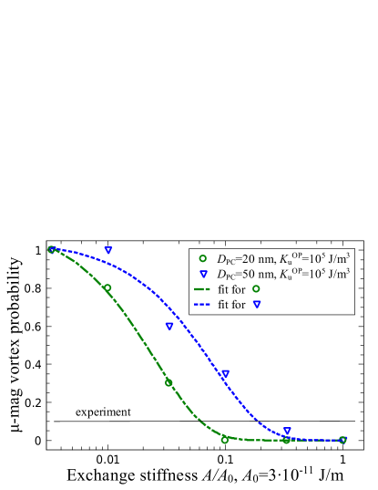
To further investigate the vortex stability in the PC we have determined the vortex nucleation probability from micromagnetic simulations where in each run the initial magnetization randomized and subsequently equilibrated. The results of these simulations for 1 nm thin disks of 10 nm and 25 nm in radius are shown in Fig. 5. The probability for each data point is an average of 20 runs and is a function of the relative exchange stiffness in the ferromagnet. The following material parameters were used: saturation magnetization A/m, anisotropy energy density J/m3, micromagnetic mesh size of 1 nm. The value of the out-of-plain uniaxial anisotropy does not change the probability significantly. The out-of-plain nature of this anisotropy can originate due to mechanical stress in the contact core, discussed in detail previously stressJAP . This simulation indicates that the experimentally observed fraction of the vortex-like PCs of 10% (black horizontal line in Fig. 5.) corresponds to a reduction in the exchange stiffness in Co of approximately one order of magnitude (5-20%, depending on the specific parameters chosen in the simulation).
We conclude that energetically distinct surface spin states play the key role in the STT effect in nano-scale magnetic PCs. These states can be uniform-spin or vortex-spin states at the surface or interface of the ferromagnet, and can be manipulated by combining the STT effects and the field of the driving current through the interface, as well as the externally applied field. Our results highlight the importance of the magnetic nature of the N/F interface, and especially the strength of the interface versus bulk exchange interaction, for the spin-dependent transport on the nanoscale.
The support of FP7 programm of EU under project STEELE 225955 and ”HAHO”-programm NAS of Ukraine under project 02/09–H is acknowledged.
References
- (1) L. Berger, Phys. Rev. B 54, 9353 (1996).
- (2) J. Slonczewski, J. Magn. Magn. Mater. 159, L1 (1996).
- (3) Y. Ji, C. L. Chen, and M. D. Stiles, Phys. Rev. Lett. 90, 106601 (2003).
- (4) M. L. Polianski and P. W. Brouwer, Phys. Rev. Lett. 92, 026602 (2004).
- (5) M. D. Stiles, J. Xiao, and A. Zangwill, Phys. Rev. B 69, 054408 (2004).
- (6) I. K. Yanson, Yu. G. Naidyuk, D. L. Bashlakov, V. V. Fisun, O. P. Balkashin, V. Korenivski, A. Konovalenko, and R. I. Shekhter, Phys. Rev. Lett. 95, 186602 (2005).
- (7) I. K. Yanson, Yu. G. Naidyuk, V. V. Fisun, A. Konovalenko, O. P. Balkashin, L. Yu. Triputen, and V. Korenivski, Nano Letters, 7, 927 (2007).
- (8) D. C. Ralph, M. D. Stiles, J. Magn. Magn. Mater. 320, 1190 (2008).
- (9) J. C. Slonczewski, J. Magn. Magn. Mater. 195, L261 (1999).
- (10) M. Gruyters, T. Bernhard, H. Winter, Phys. Rev. Lett. 94, 227205 (2005).
- (11) H. B. Zhao, D. Talbayev, G. L pke, A. T. Hanbicki, C. H. Li, and B. T. Jonker, Appl. Phys. Lett. 91, 052111 (2007).
- (12) F. J. Albert, N. C. Emley, E. B. Myers, D. C. Ralph, and R. A. Buhrman, Phys. Rev. Lett. 89, 226802 (2002).
- (13) Yu. G. Naidyuk and I. K. Yanson, Point-Contact Spectroscopy, Springer Series in Solid-State Sciences, Vol.145 (Springer Science+Business Media, Inc, 2005).
- (14) W. Rave, K. Fabian, and A. Hubert, J. Magn. Magn. Mater. 190, 332 (1998).
- (15) T. Y. Chen, Y. Ji, C. L. Chien and M. D. Stiles, Phys. Rev. Lett. 93, 026601 (2004).
- (16) M. J. Donahue and D. G. Porter, OOMMF User’s Guide, ver. 1.0, (1999); http://math.nist.gov/oommf.
- (17) T. Yang, M. Hara, A. Hirohata, T. Kimura, and Y. Otani, Appl. Phys. Lett. 90, 022504 (2007).
- (18) M. R. Pufall, W. H. Rippard, M. L. Schneider, and S. E. Russek, Phys. Rev. B 75, 140404 (2007).
- (19) Q. Mistral, M. van Kampen, G. Hrkac, Joo-Von Kim, T. Devolder, P. Crozat, C. Chappert, L. Lagae, and T. Schref, Phys. Rev. Lett. 100, 257201 (2008).
- (20) O. P. Balkashin, V. V. Fisun, I. K. Yanson, L. Yu. Triputen, A. Konovalenko, and V. Korenivski, Phys. Rev. B 79, 092419 (2009).
- (21) Details to be published elsewhere; see also K. Yu. Guslienko and K. L. Metlov, Phys. Rev. B 63, 100403 (2001); K. L. Metlov and K. Yu. Guslienko, J. Magn. Magn. Mater. 242–245 1015 (2002).
- (22) A. Konovalenko, V. Korenivski, I. K. Yanson, Yu. G. Naidyuk, V. V. Fisun, O. P. Balkashin, and L. Yu. Triputen, J. Appl. Phys. 101, 09A513 (2007)