Selecting a single orientation for millimeter sized graphene sheets
Abstract
We have used Low Energy Electron Microscopy (LEEM) and Photo Emission Electron Microscopy (PEEM) to study and improve the quality of graphene films grown on Ir(111) using chemical vapor deposition (CVD). CVD at elevated temperature already yields graphene sheets that are uniform and of monatomic thickness. Besides domains that are aligned with respect to the substrate, other rotational variants grow. Cyclic growth exploiting the faster growth and etch rates of the rotational variants, yields films that are 99 % composed of aligned domains. Precovering the substrate with a high density of graphene nuclei prior to CVD yields pure films of aligned domains extending over millimeters. Such films can be used to prepare cluster-graphene hybrid materials for catalysis or nanomagnetism and can potentially be combined with lift-off techniques to yield high-quality, graphene based electronic devices.
Graphene potentially constitutes a new material for electronic circuitry with vastly improved transport properties over traditional silicon novoselov . A large scale application of graphene crucially hinges on a fabrication method that yields perfect graphene sheets, that is low-cost and reliable. CVD growth of graphene on metals has recently been demonstrated to yield large graphene sheets of uniform monatomic thickness alpha1 ; johann ; sutter ; loginova . This form of epitaxial CVD, which occurs through ethylene decomposition on the uncovered parts of the metal substrate, is self-limiting since the nature of the process limits the thickness of the graphene sheets to a single atomic layer, in contrast to e.g. graphene formed on heated SiC substrates tromp ; emtsev . Metal CVD thus appears to be the route of choice for fabrication of large graphene sheets. In situ growth studies with LEEM and PEEM have however, highlighted a new problem. The orientation of the domains that make up the graphene sheet is not always in registry with the substrate. For the case of e.g. Ir(111), four different orientations have been observed loginova2 . The electronic properties of graphene sheets depend sensitively on the relative orientation with respect to the substrate zagreb ; kellyprl ; kellyprb . Also, applications of cluster superlattices of magnetically or catalytically active materials grown on the graphene sheets alpha2 require full control over the orientation of the domains. Here, we address this problem by tailoring the epitaxial process to grow a millimeter sized, monatomic thickness graphene sheet of single, aligned orientation.
An Ir(111) single crystal was heated to 1123 K and exposed to a mbar partial pressure of O2 to remove residual carbon contamination. CVD grwoth of graphene sheets was performed by exposing the surface to ethylene at elevated temperatures. Growth of the graphene ceases when the fractional surface coverage of graphene approaches 1 ML. Threshold PEEM images using a Hg discharge lamp yield a high intensity from the graphene flakes and very low intensity from the bare Ir(111) surface. Contrast between the different rotational domains is achieved in LEEM mode at various electron energies.
First, growth of a graphene sheet was studied at a temperature of 1411 K by exposing to an ethylene partial pressure of mbar. The formation of the graphene is shown in Fig. 1.
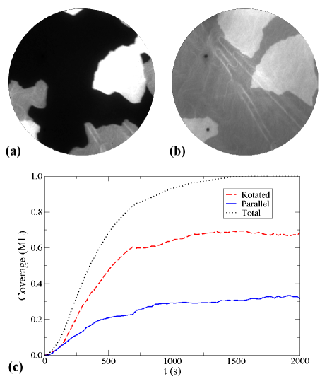
Initially, only a single phase forms that has its lattice vectors parallel to the substrate lattice. Later, graphene domains that are rotated with respect to the substrate lattice are observed to form at the edges of the original nuclei and grow at a rate that is substantially faster. In what follows, we shall refer to these as aligned and rotated domains, respectively. The structure of the graphene sheet after it has completed is shown in Fig. 1(b). From the simple observation that contrast between different domains is observed in these threshold PEEM images, we conclude that there is a significant variation of the electronic structure of the film between different domains. Even though the sheet thickness is very uniform and could already be characterized as a high quality graphene film, further control over the rotational orientation of the domains is desired.
One way to produce a high quality graphene film of a single rotational phase is done by exploiting the higher reactivity of the edges of the rotated domains. Not only do the three types of rotated domains grow at a rate that is higher than that of aligned domains, they are also etched away by oxygen at an increased rate fjmzh . Fig. 2 highlights this experimental approach.
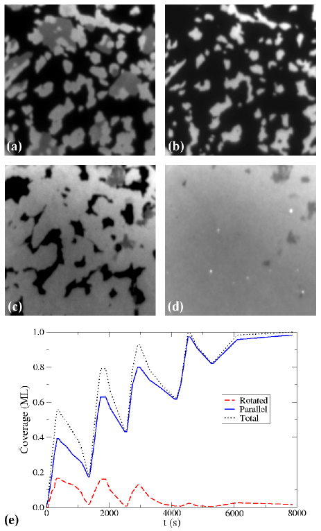
The Ir(111) surface was alternatingly exposed to ethylene and O2 at partial pressures of mbar. Exposure to ethylene leads to the formation of new nuclei and continued growth of aligned domains. It also gives rapid growth of any rotated domains that have formed. Exposure to O2, shown in Fig. 2(b), then preferentially etches away the rotated domains until only parallel domains remain. Cyclic repetition of this procedure yields a monolayer thick, near uniform graphene sheet. A relative fraction of 99 % of the sheet consists of aligned domains. The drawback of this method is that closure of the film to produce a “perfect” graphene sheet is not possible. The last step in the growth process always has to be a growth step, implying that the nucleation of rotated domains can not be fully prevented.
The nucleation of rotated domains occurs at the edges of parallel domains loginova2 . In our measurements, we also observe that growth of aligned domains and the nucleation of rotated domains occurs predominantly at those edges that do not run parallel to the substrate lattice vectors. This observation was exploited to further improve the quality of the films beyond what was demonstrated in Fig. 2 with the cyclic recipe. A monolayer of ethylene was preadsorbed on the surface at room temperature. Upon heating the substrate to the growth temperature this leads to the formation of a high density of small aligned graphene domains that have edges parallel to the substrate lattice johann . This effectively forces any graphene domains that impinge on existing nuclei to maintain their aligned orientation. Fig. 3 highlights the subsequent growth when the substrate is exposed to an ethylene partial pressure of mbar.
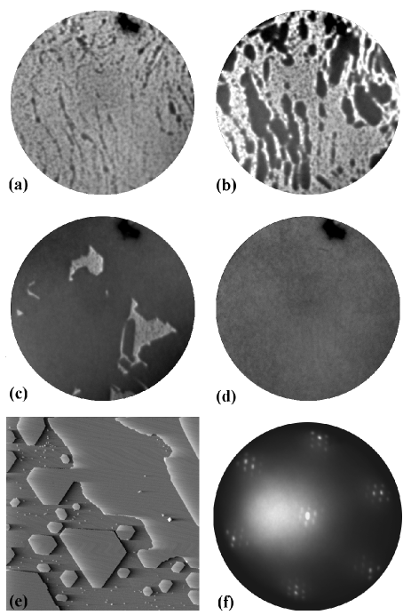
Figs. 3(b) and (c) illustrate that growth of aligned domains is observed only in those locations where domain edges are rough, having an orientation deviating from the dense packed substrate directions. Small domains with edges oriented parallel to substrate lattice vectors are not observed to grow, illustrated by the STM image shown in Fig. 3(e). Rotated domains do not form. The LEED pattern that is shown in Fig. 3(f) is measured over several millimeters of our 6 mm wide sample. Defects are sporadically found, but always in locations where we have to presume that they were induced by features present on the Ir(111) substrate. The graphene sheet that is formed through this recipe has the added advantage that its orientation is uniquely determined by the orientation of the Ir(111) substrate.
In conclusion, we have grown millimeter sized, graphene films of a single orientation. Cyclic growth of the graphene film exploiting the different growth and O2 etching speeds of the domain variants yields films that are aligned to the substrate dense packed orientation up to a fraction of 99 %. The final approach, using preadsorption of ethylene on the Ir(111) surface at room temperature, followed by CVD growth at elevated temperatures yields perfectly aligned sheets that are ready for application.
Acknowledgements.
Financial support through Deutsche Forschungsgemeinschaft is gratefully acknowledged.References
- (1) K.S. Novoselov, A.K. Geim, S.V. Morozov, D. Jiang, Y. Zhang, S.V. Dubonos, I.V. Grigorieva and A.A. Firsov, Science 306, 666 (2004).
- (2) X.K. Lu, M.F. Yu, H. Huang and R.S. Ruoff, Nanotechnology 10, 269 (1999).
- (3) A.T. N’Diaye, J. Coraux, T. Plasa, C. Busse and T. Michely, New J. Phys. 10, 043033 (2008).
- (4) J. Coraux, A.T. N’Diaye, M. Engler, C. Busse, D. Wall, N. Buckanie, F.-J. Meyer zu Heringdorf, R. van Gastel, B. Poelsema and T. Michely, New J. Phys. 11, 023006 (2009).
- (5) P.W. Sutter, J.-I. Flege and E.A. Sutter, Nat. Mater. 7, 406 (2008).
- (6) E. Loginova, N.C. Bartelt, P.J. Feibelman and K.F. McCarty, New J. Phys. 10, 093026 (2008).
- (7) R.M. Tromp and J.B. Hannon, Phys. Rev. Lett. 102, 106104 (2009).
- (8) K.V. Emtsev, A. Bostwick, K. Horn, J. Jobst, G.L. Kellogg, L. Ley, J.L. McChesney, T. Ohta, S.A. Reshanov, J. Röhrl, E. Rotenberg, A.K. Schmid, D. Waldmann, H.B. Weber and T. Seyller, Nat. Mat. 8, 203 (2009).
- (9) E. Loginova, S. Nie, K. Thürmer, N.C. Bartelt and K.F. McCarty, submitted to Phys. Rev. B (2009).
- (10) L. Pletikosić, M. Kralj, P. Pervan, R. Brako, J. Coraux, A.T. N’Diaye, C. Busse and T. Michely, Phys. Rev. Lett. 102, 056808 (2009).
- (11) G. Giovannetti, P.A. Khomyakov, G. Brocks, V.M. Karpan, J. van den Brink and P.J. Kelly, Phys. Rev. Lett. 101, 026803 (2008).
- (12) P.A. Khomyakov, G. Giovannetti, P.C. Rusu, G. Brocks, J. van den Brink and P.J. Kelly, Phys. Rev. B 79, 195425 (2009).
- (13) A.T. N’Diaye, S. Bleikamp, P.J. Feibelman and T. Michely, Phys. Rev. Lett. 97, 215501 (2006).
- (14) F.-J. Meyer zu Heringdorf et al., to be published.