Confinement of electrons in size modulated silicon nanowires
Abstract
Based on first-principles calculations we showed that superlattices of periodically repeated junctions of hydrogen saturated silicon nanowire segments having different lengths and diameters form multiple quantum well structures. The band gap of the superlattice is modulated in real space as its diameter does and results in a band gap in momentum space which is different from constituent nanowires. Specific electronic states can be confined in either narrow or wide regions of superlattice. The type of the band lineup and hence the offsets of valence and conduction bands depend on the orientation of the superlattice as well as on the diameters of the constituent segments. Effects of the SiH vacancy and substitutional impurities on the electronic and magnetic properties have been investigated by carrying out spin-polarized calculations. Substitutional impurities with localized states near band edges can make modulation doping possible. Stability of the superlattice structure was examined by ab initio molecular dynamics calculations at high temperatures.
pacs:
73.63.Nm, 73.22.-f, 75.75.+aI Introduction
Rod-like Si nanowires (SiNW) have been synthesized down to 1 nm diameter.Ma They are attractive one-dimensional (1D) materials because of the well-known silicon fabrication technology that make them directly usable on the Si-based chips. Even if unsaturated dangling bonds on the outer surface usually attribute a metallic character to SiNWs, they become insulator (or semiconductor) upon saturation of these dangling bonds by hydrogen atoms.Singh SiNWs display diversity of electronic properties depending on their diameter, as well as their orientation. In particular, the band gap of semiconductor SiNWs varies with their diameters. They can be used in various electronic, spintronic and optical applications, such as field effect transistors Cui , light emitting diodes Huang , lasers Duan and interconnects. The conductance of these semiconductor nanowires can be tuned easily by dopingdopex ; Serra during the fabrication process or by applying a gate voltage. Recent studies have shown that 3d transition metal doped Si nanowires become half-metallic.halfmetal
This letter demonstrates that SiNWs of different diameters can form stable superlattices. The electronic band structure of the superlattice is different from the constituent SiNWs and is modulated in real space leading to a multiple quantum structure and/or to a series of quantum dots. In these size induced quantum wells, specific states are confined. One dimensional multiple quantum well structures generated by compositional modulation of nanowires were examined previously. For example, superlattices of GaAs/GaP gudiksen , InAs/InP bjork and Si/SiGe wu nanowires were fabricated. Moreover, superlattices of Si and Ge were investigated theoretically.nurten In these structures multiple quantum wells are formed because of the different nature of materials that constitute the nanowire superlattice. In the present work however, multiple quantum wells are formed because of the quantum size effect, which is a diversification of the electronic structure of the same material with a change in its size.
Our results are obtained by performing first-principles plane wave calculations within Density Functional Theory (DFT)kohn using ultrasoft pseudopotentials.vander ; vasp The exchange correlation potential has been approximated by Generalized Gradient Approximation using PW91 functionalgga . A plane-wave basis set with kinetic energy cutoff of up to 250 eV has been used. All atomic positions and lattice constants are optimized. The convergence for energy is chosen as 10-5 eV between two steps, and the maximum force allowed on each atom is 0.02 eV/Å. More details about calculations can be found in Ref[halfmetal, ].
II Size Modulated Silicon Nanowires
Here Si nanowires (i.e. Si with diameter and having Si atoms in the primitive unit cell) are first cut from the ideal bulk crystal along desired direction. Then in every alternating segment comprising unit cell the diameter is kept fixed, but in the adjacent segment comprising unit cell (each having Si atoms) the diameter is reduced to . The latter part can be identified as the segment of Si nanowire. At the end, the segments of Si and Si have made a smooth junction and hence formed an ideal superlattice SiN so that its diameter is modulated in real space. Note that , because some surface atoms attaching with a single bond to the surface were removed at the beginning. Subsequently we relaxed the atomic structure of this bare SiN. Upon relaxation, the dangling bonds on the surface are saturated by H atoms and SiNHM superlattice is further relaxed for final atomic structure and the lattice constant. The resulting superlattice can be described by a Si rod with alternating diameters or a nanowire with alternating wide and narrow parts. Here we consider two superlattice structures, namely Si138H42 and Si157H64, which are grown in [111] and [100] directions, respectively. For the latter we investigate the surface defect and also boron, B and phosphorus, P substitutional impurities.
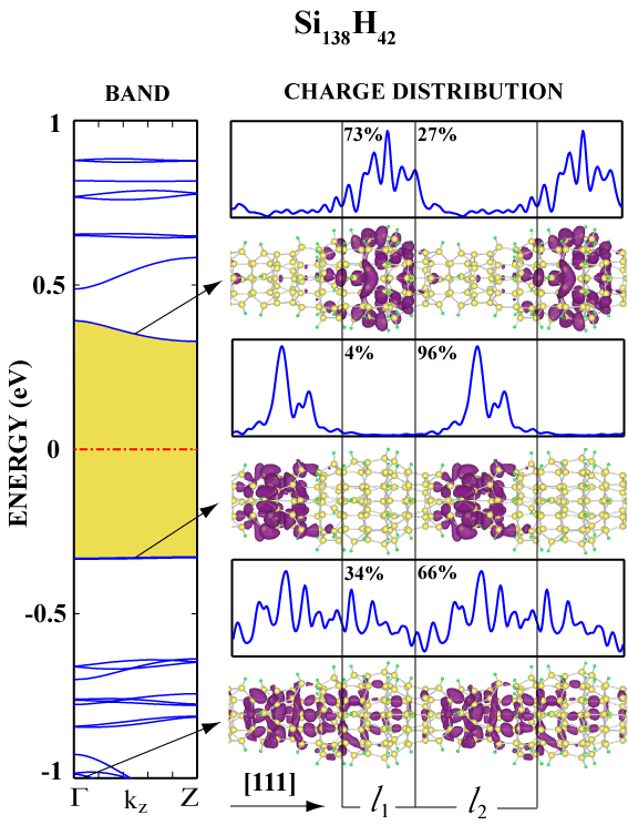
II.1 Si138H42 Superlattice
To form the superlattice, Si138H42, we took unitcell of Si68 and unitcell of Si38 cut in [111] direction of the bulk silicon crystal. The combined structure had six Si atoms attached to the surface by only one bond. These atoms were removed at the beginning and the structure was optimized. After the relaxation, all Si atoms were at least triply coordinated. The dangling bonds of triply coordinated Si atoms were saturated with hydrogen atoms and the structure was relaxed again. The band structure and isosurface charge densities of the resulting superlattice is shown in Fig. 1. Propagating states, with dispersive bands have charge densities distributed everywhere in the superlattice rod. For example, a state near -1 eV is a propagating state. The states of flat degenerate band at the top of the valence band are confined in the narrow segment. The integral of the planarly averaged charge, indicates a rather strong confinement. The states of the lowest conduction band with low dispersion are localized in the wide segment with relatively weaker confinement. This situation implies the staggered band alignment with confined hole states in the narrow part and confined electrons in the wide part. Confinement may increase with the size (length) of the confining segment since the energy of the state relative to the barrier varies. For perfect localization, i.e. 100 confinement in or , where coupling between confined states are hindered, the segment or behaves as a quantum dot. Confinement and band edge alignment in the present superlattice are reminiscent of the 2D pseudomorphic or commensurate semiconductor superlattices.Esaki
II.2 Pristine Si157H64 Superlattice and Vacancy
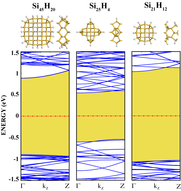
Here we presents the superlattice formation and confined states in a different structure, namely Si157H64. To form this structure we took unitcell of Si45 and unitcell of Si25 cut in [100] direction of the bulk silicon crystal. The combined structure had eight silicon atoms that were attached to the surface by only one bond. We have removed these atoms at the beginning and relaxed the resulting structure. Then we have passivated the dangling bonds of the final structure and relaxed the whole structure again. As a result, the wide part of the nanowire superlattice had unitcell of Si45H20 with 14 and the narrow part had unitcell of Si25H4 and Si21H12 mixture with 7 . Figure 2 presents the band structure of the corresponding infinite periodic nanowires which constitute the Si157H64 superlattice structure. To compare with the band structure of the superlattice (presented in Fig. 3 as pristine), the band structure of these nanowires were folded times. One can see that the band gap of the superlattice is close to the lowest band gap of its constituents. This is expected for the superlattice structures having normal band lineup. The band gaps of structures shown in Fig. 2 do not obey the well-known trend, , occurring due to the quantum confinement effectconfine at small . We ascribe this result to the surface reconstructions which differ in accordance with the procedure of atomic relaxation. Quantum confinement trend occurs when Si nanowires, cut from ideal bulk, are directly passivated with H atoms and subsequently relaxed. In the present study, however, the ideal structures are first relaxed, then passivated with H atoms and then relaxed again to obtain the final structure.halfmetal Such Si nanowire structures with D1 nm may not obey the quantum confinement trend. The decline of the gap values from the behaviour has been also reported for other types of SiNWs and was attributed to surface effects.ponomareva
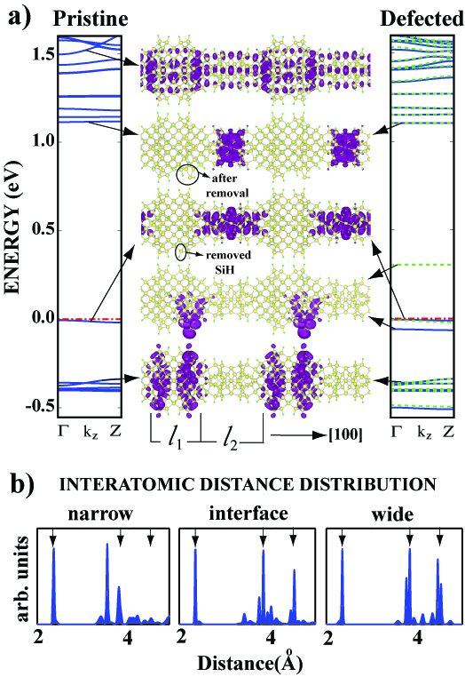
Figure 3(a) presents the band structure and the projected charge density isosurface plots of pristine Si157H64 and defected Si156H63 nanowire superlattices. Flat minibands of Si157H64 structure near the edge of conduction and valence bands are distinguished.Esaki In contrast to propagating states of dispersive bands near 1.5 eV, the states of these flat mini bands are confined in the narrow segments of the superlattice. This situation also implies a normal band lineup. We are aware of the fact that fabrication of nanowire superlattices having ideally tapered as in our case is impossible. So we examined the effect of an imperfection on the behavior of the system by removal of a Si-H atom pair, which was normally attached to the surface. The location of this defect and structural change after relaxation is given in Figure 3(a). The resulting structure has odd number of electrons, so we made spin polarized calculation. One can see that the valence and conduction band edges are not affected by defect formation, while one empty and one filled state localized around the defected area appear near the valence band edge. The magnetic moment induced by the defect formation is 1 . The vacancy states in bulk Si are located deep in the band gap. In the superlattice structure, this vacancy state is located near the valence band, since the defect is formed on the surface at the interface between two segments having different diameters.
In Figure 3(b) the distribution of interatomic distances shows significant reconstruction and deformation. In particular, owing to increased surface/volume ratio the deviation of the second and third nearest neighbour distances from the bulk crystal is rather large at the narrow and interface regions. We note that in both short periodicity superlattices discussed above the electronic structures are significantly different from the constituent SiNWs. As and/or increases, the superlattice effects and confined states may become more pronounced, and band-offset converges to a well-defined value. When the lengths of and (Broglie wavelength), the electronic properties in each segment becomes close to those in constituent nanowires. In addition to and , and and also the direction of growth are also critical parameters, since the electronic structure of the constituent SiNWs is strongly dependent on these parameters. As and increases, the surface effects decrease and the density of states becomes more bulk like. The discontinuities of valence and conduction bands of the superlattice is expected to diminish, since the band gap of the constituent nanowires converge to the bulk Si value. However for a significant the superlattice effects, in particular confinement of specific states are expected to continue. In contrast, smooth interfaces leading to hornlike profiles can be used for focused electron emission.ciraci Recently, transport properties of size modulated SiNWs have been shown to depend on the growth direction.nanoletter
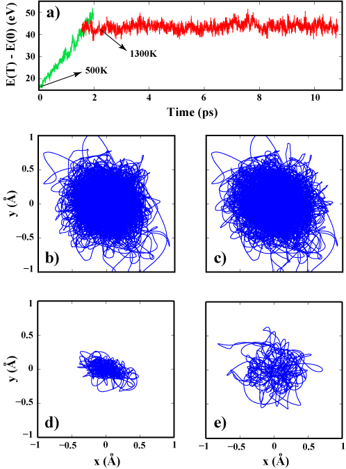
The stability of the Si157H64 structure was analyzed using the finite temperature ab initio molecular dynamics calculations with time steps of seconds. Figure 4(a) presents the total energy difference of the system with respect to the ground state energy at 0 K as a function of time. In the first calculation we have raised the temperature of the system from 500 K to 1400 K in 2 ps. During this calculation there was no major change in the structure and the interface region was not destroyed by diffusion. In the second calculation we took atomic positions and velocities of the system from the first calculation when the system was at 1300 K and kept the temperature constant for 9 ps. This calculation also resulted in no major change in the structure of the superlattice. Figure 4(b) and (c) present the path of Si atoms during the second calculation at the surfaces of wide and narrow parts respectively. The range of the thermal fluctuations are nearly the same and span a diameter of about 1 . Figure 4(d) and (e) present the path of Si atoms at the center of the wide and narrow parts respectively. As seen the range of thermal fluctuations in the narrow part () is larger than that in the wide part (). It should be noted that, the temporal trajectories of 9 picoseconds in the present ab initio molecular dynamics calculations are rather long as compared to ones usually carried out in the stability tests, but may not be long enough to accumulate necessary statistics. However, the temporal trajectories at temperature as high as 1300 K in the present study are long enough to eliminate the existence of any atomic configuration in a weak local minimum of the Born-Oppenheimer surface, which is prone to structural instability. Therefore, based on the accurate structure optimization and temporal trajectories as long as 9 picoseconds carried out at 1300 K, we believe that superlattice structure under study is stable at least at a temperature higher than the usual operation temperature (425 K) of a device.
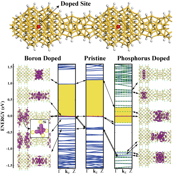
II.3 B and P doping of Si157H64 Superlattice
Next we examine the effect of doping of the Si157H64 superlattice by substitutional B and P impurities. Both structures have odd number of electrons and hence spin polarized calculations have been carried out. Nevertheless, B doped structure resulted in a nonmagnetic state with half filled band edge. P doped structure resulted in a magnetic state with a magnetic moment of 1. In Fig. 5 the electronic structure of pristine and doped superlattices are shown to follow the effect of the doping on the states at the band edges. Owing to the small diameter of the superlattice, the band structure is affected by the impurity. Since the band gap of the wide part is larger than that of the narrow part, the state associated with the impurity, which occurs normally either near the valence or conduction band, falls in the bands of the narrow part.
It is known that substitutional B doping of bulk silicon crystal results in an acceptor state 45 meV above the valence band edge.handbook In the substitutional doping of the superlattice by B similar situation occurs and the acceptor state is located above the valence band edge corresponding to the wide part, but falls in the valence band of the narrow part. The filled first and the lower lying three valence bands at about -0.4 eV undergo changes: The filled first valance band having states confined in the narrow part becomes half-filled. Three lower lying valence bands of the pristine superlattice are raised towards the edge of the valence band edge. The states of these bands mix with the tetrahedrally coordinated hybridized orbitals of B and form a triply degenerate state, just below the half filled valence band edge. Charge density isosurfaces of these states around boron atom presented in Fig. 5 clearly indicates hybridization in tetrahedral directions. As a result, the ”hole like states” becomes confined in the narrow part. As for the conduction band is slightly shifted down, but its states preserve their character.
In P doping of the superlattice at the center of the wide part, the impurity state localized at P atom occurs in the conduction band of the superlattice. This state, in fact, the donor state occurring 200 meV below the conduction band corresponding to the wide part. This energy is in good agreement with the energy calculated recently for the ionization energy of P donor states in the Si nanowires.doping Below this donor state, all conduction band states are confined either in the narrow part or at the interface, but not in the wide part. Energy shifts of the band edge states are more pronounced in structure having substitutional P doping. Conduction band edge is shifted down by 0.75 eV, but the charge density profile remains the same. One spin-up and one spin-down bands split by 0.2 eV are formed near the conduction band edge with charge densities localized in the narrow part. The triply degenerate state in the valance band near the edge are shifted down. That states localized around substitutional P impurity appear in the conduction band continua, while a filled spin up band states are localized in the defect free narrow part, indicate the possibility of modulation doping. In closing this section we note that the electronic structure associated with the doping of the small diameter superlattices is complex and has aspects different from that in the doping of bulk Si. The small size and dimensionality of the doped superlattices hinders the application of the effective mass approximation leading to hydrogenic impurity model. For the same reason, the relative positions of band edges can be affected by the presense of a substitutional impurity.
III Conclusion
In conclusion, we considered two specific superlattices grown in different crystallographic directions as a proof of concept. Each superlattice can be viewed to form the periodically repeating junctions of two hydrogen saturated silicon nanowires of different diameters. Since the band gaps of the constituent Si nanowires are different, the band gaps of these superlattices are modulated in real space. As a result, one dimensional multiple quantum well structures with states confined in different (wide or narrow) parts are formed. At strong confinement or localization, the superlattice structures can be viewed as a series of quantum dots. We believe that the bad gap modulation and resulting quantum well structure and confinement can occur as long as the band gap differences are maintained between adjacent region at both sides of the junction. Furthermore, we showed that the electronic structure resulting from the substitutional doping of the superlattice interesting and give rise to modulation doping. We finally note that, the band gaps of SiNWs at both sides of junction forming the superlattice structure are underestimated by DFT/GGA calculations. Since the systems under study are too large, these bands cannot be improved by GW calculations. Nevertheless, our work is just a proof of concept. According to our results, if the band gaps are different in different parts of the heterostructure, confined states can occur and modulation doping of these quantum structures can be achieved. Details of energy band structure and location of impurity states in the gap should only be taken qualitatively.
Various types of electronic devices, such as resonant tunnelling double barriers generated from these superlattices, can be arranged on a single rod, where they can be connected by the metallic segments of unsaturated Si nanowires. The character of these devices can be engineered by varying their growth direction and structural parameters, such as , , , . Even if the diameters of superlattices we treated in this study are small ( 1 nm) and hence in the range where band gaps vary significantly with diameter, they are still in the range of those fabricated recently.Ma
IV Acknowledgement
Part of the computations have been carried out by using UYBHM at Istanbul Technical University through a grant (2-024-2007). This work is partially supported by TÜBA, Academy of Science of Turkey.
References
- (1)
- (2) D. D. D. Ma, C. S. Lee, F. C. K. Au, S. Y. Tong and S. T. Lee, Science 299, 1874 (2003).
- (3) A. K. Singh, V. Kumar, R. Note and Y. Kawazoe, Nano Lett. 6, 920 (2006).
- (4) Y. Cui, Z. Zhong, D. Wang, W. U. Wang and C. M. Lieber, Nano Lett. 3, 149 (2003).
- (5) Y. Huang, X. F. Duan and C. M. Lieber, Small 1, 142 (2005).
- (6) X. F. Duan, Y. Huang, R. Agarwal and C. M. Lieber, Nature (London) 421, 241 (2003).
- (7) Y. Cui, X. F. Duan, J. Hu, and C. M. Lieber, J. Phys. Chem. B, 104, 5213-5216 (2000).
- (8) M. V. Fernandez-Serra, Ch. Adessi and X. Blase, Phys. Rev. Lett. 96, 166805 (2006).
- (9) E. Durgun, D. Cakir, N. Akman, and S. Ciraci, Phys. Rev. Lett. 99, 256806 (2007); E. Durgun, N. Akman, and S. Ciraci, Phys Rev. B 78, 195116 (2008).
- (10) M. S. Gudiksen, L. J. Lauhon, J. Wang, D. C. Smith and C. M. Lieber, Nature 415, 617 (2002).
- (11) M. T. Bjork, B. J. Ohlsson, T. Sass, A. I. Persson, C. Thelander, M. H. Magnusson, K. Deppert, L. R. Wallenberg, and L. Samuelson, Nano Lett.2, 87 (2002).
- (12) Y. Wu, R. Fan, and P. Yang, Nano Lett.2, 83 (2002).
- (13) N. Akman, E. Durgun, S. Cahangirov and S. Ciraci, Phys. Rev. B 76, 245427 (2007).
- (14) W. Kohn and L. J. Sham, Phys. Rev. 140, A1133 (1965); P. Hohenberg and W. Kohn, Phys. Rev. B 76, 6062 (1964).
- (15) D. Vanderbilt, Phys. Rev. B 41, R7892 (1990).
- (16) G. Kresse, J. Hafner, Phys Rev. B 47, R558 (1993); G. Kresse, J. Furthmuller, Phys Rev. B 54, 11169 (1996).
- (17) J. P. Perdew, J. A. Chevary, S. H. Vosko, K. A. Jackson, M. R. Pederson, D. J. Singh, and C. Fiolhais, Phys. Rev. B 46, 6671 (1992).
- (18) L. Esaki and L. L. Chang, Phys. Rev. Lett. 33, 495 (1974); Highlights in Condensed Matter Physics and Future Prospects, Edited by L. Esaki, Nat. Science Forum Series B, Volume 285, Plenum Press 1991.
- (19) X. Zhao, C.M. Wei, L. Yang and M.Y. Chou, Phys. Rev. Lett. 92, 236805 (2004); M. Bruno, M. Palummo, A. Marini, R. DelSole and S. Ossicini, Phys. Rev. Lett. 98, 036807 (2007); R. Rurali, B. Aradi, Th. Frauenheim and A. Gali, Phys. Rev. B 76, 113303 (2007)
- (20) I. Ponomareva, E. Richter, A.N. Andriotis and Madhu Menon, Nano Lett. 7, 3424 (2007).
- (21) S. Ciraci and I. P. Batra, Phys. Rev. B 36, 6194 (1987); E. Tekman, S. Ciraci and A. Baratoff, Phys. Rev. B 42, 9221 (1990).
- (22) M. P. Persson, A. Lherbier, Y. Niquet, F. Triozon and S. Roche, Nanoletters, DOI: 10.1021/nl801128f (2008).
- (23) Handbook of Semiconductor Silicon Technologi, Edited by W.C. O’Mara, R.B. Herring, and L.P. Hunt, Noyes Publications (1990).
- (24) M. Diarra, Y-M. Niquet, C. Delerue and G. Allan, Phys. Rev. B 75, 045301 (2007);T.-L. Chan, M.L. Tiago, E. Kaxiras and J.R. Chelikowsky, Nano Lett. 8, 596 (2008);C.R. Leao, A. Fazzio and a.J.R. daSilva, 8 1866 (2008).