Monolayer honeycomb structures of group IV elements and III-V binary compounds
Abstract
Using first-principles plane wave calculations, we investigate two dimensional honeycomb structure of Group IV elements and their binary compounds, as well as the compounds of Group III-V elements. Based on structure optimization and phonon mode calculations, we determine that 22 different honeycomb materials are stable and correspond to local minima on the Born-Oppenheimer surface. We also find that all the binary compounds containing one of the first row elements, B, C or N have planar stable structures. On the other hand, in the honeycomb structures of Si, Ge and other binary compounds the alternating atoms of hexagons are buckled, since the stability is maintained by puckering. For those honeycomb materials which were found stable, we calculated optimized structures, cohesive energies, phonon modes, electronic band structures, effective cation and anion charges, and some elastic constants. The band gaps calculated within Density Functional Theory using Local Density Approximation are corrected by GW0 method. Si and Ge in honeycomb structure are semimetal and have linear band crossing at the Fermi level which attributes massless Fermion character to charge carriers as in graphene. However, all binary compounds are found to be semiconductor with band gaps depending on the constituent atoms. We present a method to reveal elastic constants of 2D honeycomb structures from the strain energy and calculate the Poisson’s ratio as well as in-plane stiffness values. Preliminary results show that the nearly lattice matched heterostructures of these compounds can offer new alternatives for nanoscale electronic devices. Similar to those of the three-dimensional Group IV and Group III-V compound semiconductors, one deduces interesting correlations among the calculated properties of present honeycomb structures.
pacs:
73.22.-f, 61.48.De, 63.22.-m, 62.23.KnI introduction
Last two decades, nanoscience and emerging nanotechnologies have been dominated by honeycomb structured carbon based materials in different dimensionality, such as fullerenes, single and multi walled carbon nanotubes, graphene and its ribbons. In particular, graphene, a two dimensional (2D) honeycomb structure of carbon, has been an active field of research.novo Because of unique symmetry, electron and hole bands of graphene show linear band crossing at the Fermi levelwallace resulting in a massless Dirac Fermion like behavior of charge carriers. As a result, Klein paradox, an interesting result of quantum electrodynamics was expected to be observed in graphene.kats ; novo2 ; itzykson and zuber ; calogeracos Moreover, it was shown that half-integer quantization of Hall conductancenovo2 ; zhang ; berger can be observed in graphene. Unusual electronic and magnetic properties of graphene, such as high carrier mobility, ambipolar effect, have promised variety of applications. In addition to some early works on crystalline order in planar structures,mermin ; doussal possibility of very large one-atom-thick two dimensional (2D) crystals with intrinsic ripples is reported theoreticallykastnelson-nature and experimentally.meyer Not only extended 2D graphene sheets but also quasi-one-dimensional graphene ribbons with armchair or zigzag edges have shown unusual electronic,son ; barone ; areshkin ; sasaki ; abanin ; ezawa magnetickobayashi ; fujita ; nakada1 ; wakabayashi1 and quantum transport properties.graphene_applications2 ; graphene_applications4 ; jie ; hasan
All these experimental and theoretical studies on graphene created significant interest in one-atom-thick honeycomb lattices of other Group IV elements and compounds of III-V and II-VI Group elements. Recently, the boron-nitride (BN) honeycomb sheet was reported as a stable ionic monolayer.bn-synthesis BN has the same planar structure as graphene with a nearest neighbor distance of 1.45 Å. However, its ionic character causes a gap opening at the K-point. Thus, instead of being a semimetal, BN honeycomb structure is a wide band gap insulator with an energy gap of 4.64 eV. Soon after its synthesis, several studies on nanosheets bn-nanosheets1 and nanoribbonsGuo ; louie-nanoletter ; barone2 ; bn-mehmet of BN have been reported.
Hexagonal monolayer of Zinc Oxide (ZnO) is a II-VI metal-oxide analogue of graphene and BN. Previously, works on nanostructures of ZnO such as nanosheets,znosheet nanobelts,znobelt nanotubes,znotube nanowiresznowire and nanoribbonsznomehmet were reported and recently the synthesis of ZnO bilayer honeycomb structure was also achieved.znobilayer In contrast to graphene, ZnO nanoribbons have ferromagnetic order in their ground state due to electronic states at the zigzag edges dominated by oxygen atoms.mendez1 ; mendez2
Two dimensional SiC honeycomb sheet is another Group IV binary compound displaying interesting properties. While the infinite periodic 2D form of SiC is a semiconductor with 2.55 eV band gap, and its zigzag nanoribbons are magnetic metals, the armchair ribbons are nonmagnetic semiconductors.sic Half-metallicity is also predicted for narrow SiC zigzag nanoribbons without any chemical decoration or applied external field. Furthermore, functionalization of SiC single sheets upon formation of various types of vacancies and adatom decoration was also predicted.erman-sic
Very recently, we have reported that among Group IV elements, not only C but also Si and Ge can form stable honeycomb structures.Si It is found that for Si and Ge planar (PL) geometry is not the lowest energy configuration and it is not stable. Alternatively, it was shown that a low-buckled (LB) (or puckered) geometry corresponds to a stable local minimum on the Born-Oppenheimer surface. Buckled honeycomb structure of Si was pointed out even in some earlier studies.takeda ; durgun ; zhang Surprisingly, in spite of their puckered geometrical structure, Si and Ge monolayers have electronic band structures which are similar to graphene. As a result, linear crossing of - and -bands at K- and K’-points of the hexagonal BZ attributes a massless Dirac fermion character to the charge carriers. Quasi 1D honeycomb structures, namely nanoribbons of Si and Ge, also show interesting electronic and magnetic properties depending on their width and orientation. Successful realization of single crystal silicon monolayer structuresnakamura ; krishnan through chemical exfoliation shows that 2D silicon monolayers with their low resistivity and extremely thin structures can be quite promising for nanoelectronics.
| (eV) | C (J/m2) | ||||||||||||
| LDA | |||||||||||||
| Graphene | PL | 120.0 | - | 1.42 | 2.46 | 20.08 | semimetal | 0.0/0.0 | 0.16 | 335 | |||
| Si | LB | 116.4 | 0.44 | 2.25 | 3.83 | 10.32 | semimetal | 0.0/0.0 | 0.30 | 62 | |||
| Ge | LB | 113.0 | 0.64 | 2.38 | 3.97 | 8.30 | semimetal | 0.0/0.0 | 0.33 | 48 | |||
| SiC | PL | 120.0 | - | 1.77 | 3.07 | 15.25 | 2.52/KM-3.89/KM | 1.53/6.47 | 0.29 | 166 | |||
| GeC | PL | 120.0 | - | 1.86 | 3.22 | 13.23 | 2.09/KK-3.56/KK | 2.82/5.18 | 0.33 | 142 | |||
| SnGe | LB | 112.3 | 0.73 | 2.57 | 4.27 | 8.30 | 0.23/KK-0.41/KK | 3.80/4.20 | 0.38 | 35 | |||
| SiGe | LB | 114.5 | 0.55 | 2.31 | 3.89 | 9.62 | 0.02/KK-0.00/KK | 3.66/4.34 | 0.32 | 57 | |||
| SnSi | LB | 113.3 | 0.67 | 2.52 | 4.21 | 8.72 | 0.23/KK-0.69/KK | 3.89/4.11 | 0.37 | 40 | |||
| SnC | PL | 120.0 | - | 2.05 | 3.55 | 11.63 | 1.18/K-6.01/K | 2.85/5.15 | 0.41 | 98 | |||
| BN | PL | 120.0 | - | 1.45 | 2.51 | 17.65 | 4.61/KK-6.57/K | 0.85/7.15 | 0.21 | 267 | |||
| AlN | PL | 120.0 | - | 1.79 | 3.09 | 14.30 | 3.08/M-5.74/M | 0.73/7.27 | 0.46 | 116 | |||
| GaN | PL | 120.0 | - | 1.85 | 3.20 | 12.74 | 2.27/K-4.58/K | 1.70/6.30 | 0.48 | 110 | |||
| InN | PL | 120.0 | - | 2.06 | 3.57 | 10.93 | 0.62/K-5.35/ | 1.80/6.20 | 0.59 | 67 | |||
| InP | LB | 115.8 | 0.51 | 2.46 | 4.17 | 8.37 | 1.18/K-2.68/K | 2.36/5.64 | 0.43 | 39 | |||
| InAs | LB | 114.1 | 0.62 | 2.55 | 4.28 | 7.85 | 0.86/-1.92/ | 2.47/5.53 | 0.43 | 33 | |||
| InSb | LB | 113.2 | 0.73 | 2.74 | 4.57 | 7.11 | 0.68/-1.71/ | 2.70/5.30 | 0.43 | 27 | |||
| GaAs | LB | 114.7 | 0.55 | 2.36 | 3.97 | 8.48 | 1.29/K-2.77/K | 2.47/5.53 | 0.35 | 48 | |||
| BP | PL | 120.0 | - | 1.83 | 3.18 | 13.26 | 0.82/KK-1.67/KK | 2.49/5.51 | 0.28 | 135 | |||
| BAs | PL | 120.0 | - | 1.93 | 3.35 | 11.02 | 0.71/KK-1.14/KK | 2.82/5.18 | 0.29 | 119 | |||
| GaP | LB | 116.6 | 0.40 | 2.25 | 3.84 | 8.49 | 1.92/K-3.50/KM | 2.32/5.68 | 0.35 | 59 | |||
| AlSb | LB | 114.8 | 0.60 | 2.57 | 4.33 | 8.04 | 1.49/KM-2.01/KK | 1.58/6.42 | 0.37 | 35 | |||
| BSb | PL | 120.0 | - | 2.12 | 3.68 | 10.27 | 0.39/KK-0.23/KK | 3.39/4.61 | 0.34 | 91 |
Motivated by the recent experimental developments and theoretical investigations on 2D monolayer honeycomb structures, in this paper we carried out a systematic study of similar structures of Group IV elements and III-V binary compounds based on first principles calculations within Density Functional Theory (DFT). Our objective is to reveal whether monolayer honeycomb structures can be found as a local minimum on the Born-Oppenheimer surface. We hope that the predictions of our work will guide further experimental studies towards the synthesis of new materials having honeycomb structure. The present work, which considers a total of 26 elemental and binary compounds in 2D honeycomb structure and reveals whether they are stable, is an extension to our preliminary work on Si and Ge puckered honeycomb structures. Si Based on extensive analysis of stability, 22 different materials out of 26 are found to be stable in a local minimum on the Born-Oppenheimer surface either in finite size or in infinite periodic form. We hope that interesting properties predicted by this study will promote efforts towards synthesizing new materials and heterostructures, which will constitute a one-dimensional analogue of 3D family of tetrahedrally coordinated semiconductors.
The organization of this paper is as follows; In Sec. II the methods together with parameters used in our calculations are outlined. In Sec. III, we determine the atomic structure and related lattice constants of the honeycomb structures via total energy minimization. We also discuss how the stability of the structure is maintained through puckering. In the same section, we present our results regarding the calculation of phonon modes and our analysis of stability based on these results. The mechanical properties of these structures are investigated in Sec. IV. We discuss the electronic band structure of various stable materials calculated within DFT in Sec. V. The underestimated band gaps are corrected by using GW0 calculations. As a proof of concept for a possible future application of these materials we consider semiconductor superlattices formed from the periodically repeating pseudomorphic heterostructure in Sec VI. We showed that the superlattices have an electronic structure different from those of constituent materials and behave as multiple quantum well structures with confined states. In Sec. VII, our conclusions are presented.
II Methods
We have performed self-consistent field, first-principles plane-wave calculationsvasp1 ; vasp2 within DFT for total energy and electronic structure calculations. Projector augmented wave (PAW) potentialsblochl and exchange-correlation potentials approximated by local density approximationlda (LDA) are used in our calculations. In the self-consistent field potential and total energy calculations a set of (25x25x1) k-point sampling is used for Brillouin Zone (BZ) integration in k-space. Kinetic energy cutoff for plane-wave basis set is taken as 500 eV . The convergence criterion of self consistent calculations is eV for total energy values. By using the conjugate gradient method, all atomic positions and unitcell were optimized until the atomic forces were less than 0.05 eV/Å. Pressures on the lattice unit cell are decreased to values less than 0.5 kB. To prevent interactions between the adjacent supercells a minimum of 10 vacuum spacing is kept.
To correct the energy bands and band gap values obtained by LDA, frequency-dependent GW0 calculations are carried out.gw Screened Coulomb potential, W, is kept fixed to initial DFT value W0 and Green’s function, G, is iterated five times. Various tests are performed regarding vacuum level, kinetic energy cut-off potential, number of bands, k-points and grid points. Final results of GW0 corrections are obtained by using (12x12x1) k-points in BZ, Å vacuum spacing, default cut-off potential for GW0, 160 bands and 64 grid points.
Cohesive energies () per pair of atoms (see Table 1) are calculated by using the expression
| (1) |
where is the total energy per A-B pair of the optimized honeycomb structure; and are the total energies of free A and B atoms. All of them are calculated in the same cell. For graphene, Si and Ge, . For the charge transfer analysis, the effective charge on atoms are obtained by Bader method.bader In fact, various methods for charge transfer analysis give similar trends for the honeycomb structures studied in this paper. For rigorous test of the stability of fully relaxed honeycomb structures under study, we also calculated phonon modes by using force constant method.alfe Here the Dynamical Matrix was constructed from forces, resulting from displacements of certain atoms in (7x7) supercell, calculated by VASP software.
III Atomic Structure
We first present a detailed analysis of two-dimensional (2D) hexagonal structure of binary compounds of Group IV elements, their binary compounds and Group III-V compounds all forming honeycomb structure. In our study, we also include the discussion of graphene, Si and Ge in honeycomb structure for the sake of comparison.
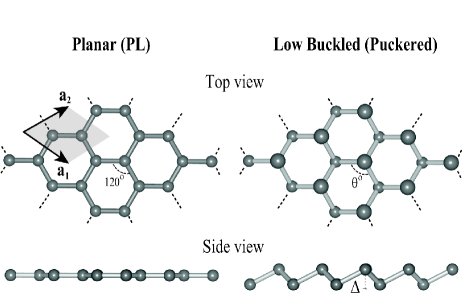
Graphene has a 2D hexagonal lattice in which C atoms are arranged to form a planar (PL) honeycomb structure as shown in Fig.1. Accordingly, it has a six fold rotation axis, at the center of the hexagon, which is perpendicular to the atomic plane. Hexagonal lattice has a two-atom basis in the primitive unit cell, corresponding to A- and B-sublattices. That is three alternating atoms of each hexagon belong to one of the two sublattices. In graphene planar geometry is assured by the formation of strong -bonding between two nearest neighbor -orbitals perpendicular to the graphene plane. The resulting - and -bands determine also relevant electronic properties. In addition, there are strong yet flexible, covalent -bonds derived from the planar hybrid orbitals between adjacent C atoms. Nearest C atoms are separated by 1.42 Å and the magnitude of the hexagonal Bravais lattice vector is 2.46 Å. Briefly, the planar hybridization and perpendicular orbitals underlie planar geometry, unusual mechanical strength and electronic structure of graphene.
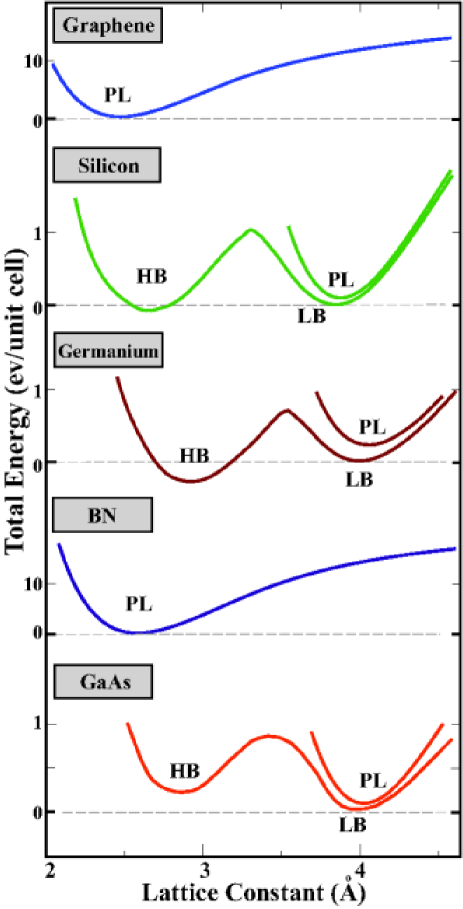
In Fig. 2 we show the variation of the total energy with respect to the lattice constant of the 2D hexagonal Bravais lattice. We see that C and BN stayed planar and have a single minimum. The situation with Si, Ge and GaAs is different, since they have two other minima corresponding to low buckled (LB) and high buckled (HB) geometries in addition to planar geometry. In fact, the total energies corresponding to the minimum of the planar geometry are already higher than those of LB and HB geometries. In buckled geometries, while atoms of A-sublattice are rising, those of B-sublattice are lowered. At the end atoms of A- and B-sublattices lie in different planes having a buckling distance, as shown in Fig. 1. The value of in HB geometry is high and is in the ranges of 2.5Å, but it is low in LB geometry and ranges between 0.4 and 0.7Å. We note that two minima corresponding to HB and LB geometries in Fig. 2 are seperated by a significant energy barrier. As we discuss in subsection III.B the minimum of HB is not actually a local minimum on Born-Oppenheimer surface. The six-fold rotation symmetry of graphene is broken as a result of buckling and changes to the three-fold rotation symmetry . The similar symmetry breaking takes place also in Group III-V compounds having PL honeycomb structures.
In concluding this discussion, we point out that even if the calculated total energy has a minimum relative to a specific structural parameter, this may not correspond to a local minimum. Then it remains to answer which of these minima in Fig. 2 corresponds to a local minima on the Born-Oppenheimer surface. At this point, reliable tests for stability of structure have to be performed.
III.1 Phonon modes and stability
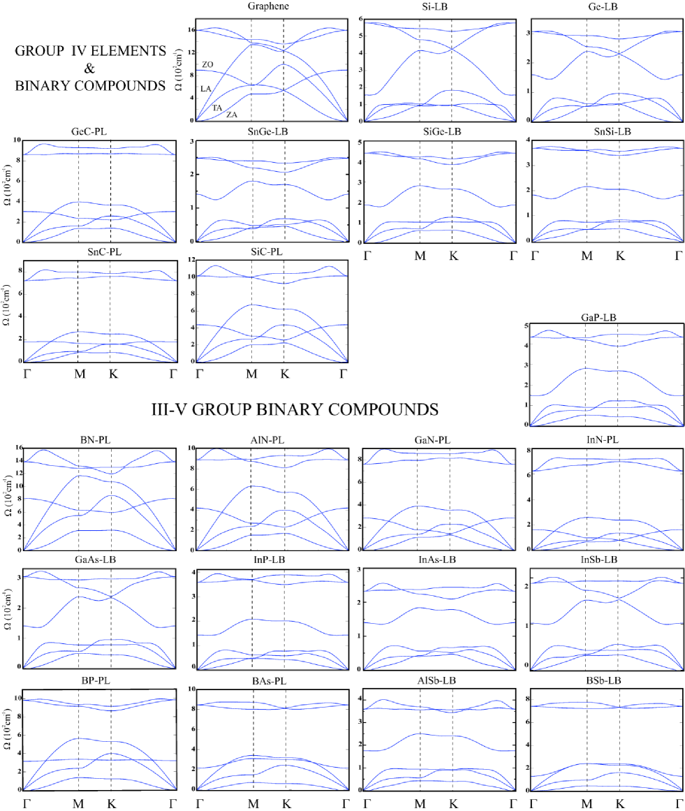
Analysis of phonon modes provides a reliable test for a structure optimized conjugate gradient method. If there is an instability related with a phonon mode with k in BZ, the square of frequency, (k) obtained from the dynamical matrix becomes negative implying an imaginary frequency. Phonon calculations are performed by taking into account the interactions in (7x7x1) large supercells consisting of 98 atoms. For all the infinite 2D honeycomb structures there are three acoustical (A) and three optical (O) modes. In Fig. 3, we present the calculated dispersions of phonon modes of various honeycomb structures; namely Group IV elements and their binary compounds, as well as Group III-V compounds. According to these results some materials, for example Sn cannot be stable in the honeycomb structure. None of the honeycomb structures are stable in the HB geometry. Only 22 honeycomb structures studied in this paper display (k) dispersions, which confirm their stability either in PL or in LB geometry.
Well known linear behavior of phonon dispersions of LA and TA branches and quadratic behavior of ZA branch around -point also exist for all 2D lattices. Among these, the LA and TA phonon branches are heat carrying modes. However, it was shown that bending branch ZA makes negligible contribution to thermal conductivity.klemens Note that only the ZA branch gets imaginary frequencies for k wave vectors in the vicinity of -point in BZ. While this indicates the structural instability for infinitely large periodic structures, it can be taken also as evidence that an infinitely large 2D hexagonal lattice can be stabilized by defects or ripples with large wave length. Our analysis for such systems treated in () supercells showed the existence of ripples. Clearly, finite patches of such structures can become stable. This argument has been confirmed by our calculation of vibration modes of finite size patches.
In our earlier paperSi we found that ZA mode of 2D periodic Ge honeycomb gets imaginary frequencies near -point of BZ. This situation has been interpreted as the instability against long wavelength transversal waves, which can be stabilized by rippling or by limiting the size of Ge sheets. An extensive analysis of phonon modes in the present study revealed that the extent of the region of imaginary frequencies around the -point also depends on the mesh size used in the calculations. Decreasing the mesh size may lead to the decreasing of their particular zone. Therefore, a tedious analysis of the right mesh size is required to determine whether or not the imaginary frequency zone of ZA mode is an artifact of the mesh size. We performed this analysis of mesh size for Ge-LB structure and found an optimum fine mesh size where imaginary frequencies of ZA mode disappeared. We also note that since the interatomic forces related with ZA modes decay rapidly, the numerical inaccuracy in calculating forces due to the transversal displacement of distant atoms may give rise to difficulties in the treatment of ZA modes. Briefly, caution has to be exercised in deciding whether the imaginary frequencies of ZA modes is an artifact of numerical calculations. Of course, if the presence of imaginary frequencies near the -point is a reality, the instability of infinite and 2D periodic structures can be stabilized by finite size or large wavelength ripplings.
Calculated phonon dispersion of graphene is in good agreement with previous LDA results and also with reported experimental data.ihlee ; narasimhan ; yan Around 1600 , LO and TO eigenmodes are degenerate at point. In-plane TA and LA eigenmodes have linear dispersion around the point. As it is mentioned in earlier works on 2D structures, out-of-plane ZA eigenmode have quadratic phonon dispersion in the vicinity of -point. Here, the calculated value for out-of-plane optical eigenmode ZO is around 900 . Existence of strong electron-phonon coupling in TO eigenmode at the -point and modes at -point is the reason of the Kohn anomaly at these points. Therefore, scattering by phonon with the energies that corresponds to these modes can cause noticeable decrease in transmission spectrum.yan ; pisanec Since force constant decreases with increasing atomic number or row number in the Periodic Table, calculated vibration frequencies exhibit the same trend.
As a result of symmetry in honeycomb structures of Group IV elements (such as graphene, Si and Ge), ZO and TO branches cross at point. We also note that the ZO branch of a binary compound comprising at least one element from the first row falls in the frequency range of acoustical vibration modes. By comparing the phonon dispersions of InN, InP, InAs and InSb samples, it is seen that ZO mode have increasing tendency to move apart from the LA and TA modes with increasing nearest neighbor distance. However, in all the samples containing first row elements, ZO mode is located between the LA and TA modes. These characteristic trends of ZO mode exists for all the 2D honeycomb structures.
III.2 Stability via Puckering
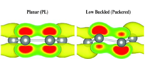
According to analysis of stability based on the calculated phonon modes, structures which do not contain first row elements occur in LB (puckered) structure corresponding to a local minimum in Born-Oppenheimer surface. Through puckering the character of the bonding changes. Different hybrid orbitals underlie the different allotrophic forms of C atom. While the bonding of diamond structure is achieved by tetrahedrally coordinated, directional hybrid orbitals, and hybrid orbitals make the bonding in graphene and cumulene (monatomic chain of carbon atoms), respectively. In forming hybrid orbitals one of two valence states is excited to state, whereby a promotion energy is implemented to the system. However, by and hybridization the hybrid orbitals yield the maximum overlap between adjacent C-C atoms and hence the strongest possible bonding. This way, the promotion energy is compensated and the system attains cohesion. In hybrid combination one orbital is combined with , and orbitals to form four orbitals directed from the central C atom towards its four nearest neighbors in tetrahedral directions. The angle between these bonds is . In one is hybridized with and orbitals to make three planar which are directed from the central C atom at the corners of the hexagons to its three nearest neighbors. For the cumulene orbital is hybridized with orbital along the chain axis. In this respect, the strengths (i.e. self-energy) of these hybrid orbitals decreases with increasing number of -type orbitals in the combination; namely is strongest whereas is least strongest. As for the the distance of C-C bonds, it is shortest in cumulene (1.29), but longest in diamond (1.53 Å). In addition to these hybrid orbitals, dangling orbitals make also -bonding between two C atoms. The -bonding between two adjacent C atoms in graphene and cumulene assures the planarity and linearity, respectively. In Fig.4 the charge density of the -bonds between neighboring C atoms explains how the stable planar geometry is maintained.
As the bond distance between two nearest neighbor atoms increases the overlap of the orbitals decreases. This, in turn, decreases the strength of the -bond. This is the situation in the honeycomb structures of Si, where the Si-Si bond distance (2.34 Å) increased by 92% relative to that of the C-C bond. As a result of weaker bonds in Si can not maintain the stability of the planar geometry, and the structure attains the stability through puckering, where three alternating atoms of a hexagon raises as the remaining three is lowered. At the end the structure is buckled by . Through buckling the hybrid orbital is dehybridized and , , orbitals are then combined with to form hybrid orbitals. While three hybrid orbitals form covalent bonds with three nearest neighbor atoms, one orbital directed upwards perpendicular to the atomic plane form a weak bond with the adjacent orbital directed downwards. Eventually, a puckered Si honeycomb structure is reminiscent of graphaneelias ; sofo ; hasan-graphane with alternating C atoms saturated with hydrogen atoms from different sites. Briefly, puckering occurs as a result of weakening of -bonds, whereby the structure regains its stability through tetrahedrally coordinated -like bonding. Puckering may be explained in terms of Jahn-Teller theoremjahn-teller predicting that an unequal population of degenerate orbitals in a molecule leads to a geometric distortion. This way the degeneracy is removed and the total energy is lowered.
As shown in Table 1, 11 out of 22 honeycomb structures prefer planar geometry, the rest is puckered to regain stability. There are interesting examples for planar and puckered ring structures: Besides BN, planar molecule and well known boric acid planar crystals are other examples for boron including materials. rings such as , and have also puckered structures with a crown shape.bmeyer Another example is planar cyclobutadiene (); the well known molecule was shown that it lowers its energy when it has puckered (butterfly) structure for its positive dianion (). Additionally, it was shown beforechem-bond-theory that puckered shape of cyclooctatetraene takes planar shape for its negative dianion . For the phosphazenes (), while is planar and have buckled shapeslabarre ; hazenkampf and thus the rule regarding the compounds including first row elements is still valid.
Having discussed the general aspects, we now concentrate on the optimized atomic structure and corresponding electronic properties of stable honeycomb structures. Calculated values of atomic and electronic structural parameters are given In Table 1. One notes that 11 structure having planar geometry has at least one constituent from the first row elements of the Periodic Table; namely C, B and N. Since the radii of these atoms are relatively small, their presence as one of the constituents assures that the bond length is small enough to keep strong -bonding. This explains how the radius of constituent atoms enters as a crucial ingredient in the structure. The rest of the honeycomb structures in Table 1 including Si and Ge are puckered to have LB geometry.
Finally, we note that calculated results given in Table 1 display interesting trends depending on the radius of constituent elements or their row number in the Periodic Table. For example, the bond strength or cohesive energy of a honeycomb structure gets weaker as the atomic radii or the row number of the constituent elements increase. Also band gap and lattice constant show similar trends.
IV Mechanical Properties
Honeycomb structure with bonding underlies the unusual mechanical properties providing very high in-plane strength, but transversal flexibility. We note that graphene and its rolled up forms, carbon nanotubes are among the strongest and stiffest materials yet discovered in terms of tensile strength and elastic modulus. We investigated the mechanical properties of 22 stable honeycomb structures listed in Table 1. We focused on the harmonic range of the elastic deformation, where the structure responded to strain linearly. We pulled the rectangular unit cell in - and -directions in various amounts and generated a mesh of data corresponding to the strains in and directions versus strain energy defined as ; namely, the total energy at a given strain minus the total energy at zero strain. The data is fitted to a two-dimensional quadratic polynomial expressed by
| (2) |
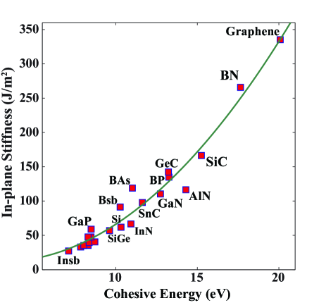
where and are the small strains along - and -directions in the harmonic region. Owing to the isotropy of the honeycomb structure . The same equation can be obtained from elastic tensornye in terms of elastic stiffness constants, namely ; . Hence one obtains Poisson’s ratio = -/, which is equal to . Similarly, the in-plane stiffness, ) = (2a1-(a3)2/2a1)/(A0). Here and are the effective thickness and equilibrium area of the system, respectively. In Table 1, calculated Poisson’s ratio and in-plane stiffness results are shown. The calculated value of the in-plane stiffness of graphene is in agreement with the experimental value of 340 (N/m).gr_exp Graphene has highest in-plane stiffness and lowest Poisson’s ration among all honeycomb structures of Group IV elements and Group III-V compounds. Being a compound of first row elements, BN has second highest and second lowest . The Poisson’s ratio increases with increasing row number of elements of elemental and compound honeycomb structures. shows a reverse trend. The order of values of in the last column of Table 1 is similar to that of cohesive energies in the seventh column. This clearly indicates a correlation between and as shown in Fig. 5.
V Electronic Structure
Our results on the electronic band structure of Group IV elements and binary compounds between different Group IV elements and Group III-V elements, which are stable in either infinite periodic form or in finite size, are presented in Fig. 6. In these hexagonal lattice structures (PL or LB) relevant electronic energy bands around the Fermi level are derived from and -bands. In elemental honeycomb structures, such as graphene, Si and Ge, these bands have linear crossings at two in-equivalent - and -points of BZ, called Dirac points and hence they are semimetallic. Because of their linear dispersion of (k), the charge carriers near the Dirac points behave as massless Dirac Fermions. By fitting the -and - bands at to the expression,
| (3) |
and neglecting the second order terms with respect to , one can estimate the Fermi velocity for both Si and Ge as . We note that calculated for 2D LB honeycomb structures of Si and Ge are rather high and close to that calculated for graphene using the tight-binding bands. It is also worth noting that because of the electron-hole symmetry at K- and -points of BZ, 2D LB Si and Ge are ambipolar for E(q)= , being small.
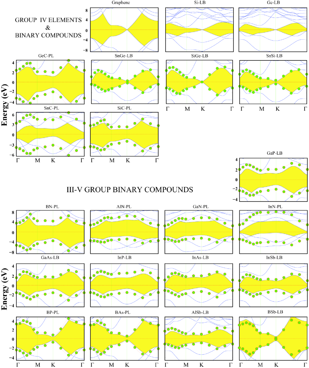
In graphene Dirac fermions have a high Fermi velocity, . Due to its high carrier mobility, graphene based ballistic transistors operating at room temperature have already been fabricated.dai-transistor In addition to these unusual electronic properties of graphene, the observation of anomalous quantum Hall effect and the possibility of Klein paradox are features, which attract the interest of researchers. Electronic properties of graphene and graphene-based structures have recently been reviewed.geim-novo2007 ; revmod
In the polar structures, such as BN, GaAs, after charge transfer orbital electrons are located predominantly on one type of atom. Thus the degeneracy of valence and conduction bands at point is removed and gap opening occurs.harrison In Table 1 the minimum width of band gaps calculated with LDA are given together with the symmetry points where the maximum (minimum) of valence (conduction) bands occur. Values of these band gaps after a correction by the GW0 method are also given. The bands of compounds before and after GW0 correction are also illustrated in Fig. 6.
Binary compounds have polar character in addition to the covalency of bonds. Effective charge on cation and anion , charge transferred from cation to anion, ( being the valency of the constituent atom) are calculated using Bader analysis. In spite of the ambiguities in finding the true effective charge, the calculated effective charges in Table 1 give some idea about the direction of charge transfer and ionicity of the honeycomb structure. For some binary compounds like SiC, BN, AlN calculated effective charges appear to be right in sign but exaggerated in magnitude. We note that as the difference in the row numbers of constituent elements increases, usually decreases. One can also generalize that the charge transfer decreases with increasing row number or atomic radii of anion if the cation is fixed. This trend is obvious in the structures of InN, InP, InAs and InSb.
VI Heterostructures
Depending on the constituent elements the band gaps of compound honeycomb structures change in a wide energy range. In contrast, the lattice constant of the compounds do not show significant variation. The situation, where band gaps of two honeycomb structures are significantly different, while their lattice constants are practically the same, is a convenient condition to make semiconductor heterostrucures. As an example, let us consider AlN and GaN, which have LDA band gaps of 3.08 eV and 2.27 eV, respectively. Their lattice constants are not significantly different and are 3.09 and 3.20 Å, respectively. Moreover, armchair nanoribbons can form pseudomorphic heterostructure with perfect junction. This is reminiscent of an AlN/GaN commensurate heterostructure having 2D interface. Owing to charge transfer between constituent nanoribbons at the junction, the bands are shifted and eventually aligned. Heterostructures of elemental and compound semiconductors generating a 2D electron gas and devices produced therefrom have been an active field of study in device physics in the past decades. It is expected that the heterostructure of armchair nanoribbons of GaN and AlN can constitute a 1D analog. When periodically repeated, this heterostructure can form superlattices behaving as multiple quantum wells or quantum dots. Earlier similar effects have been investigated for the heterostructures of graphene nanoribbons with different widths.graphene_applications4
Superlattices of armchair honeycomb nanoribbon structures can be constructed according to the width and repeat periodicity of the constituent segments. We can label GaN/AlN superlattices as GaN/AlN(,;,). Here, and specify the length of segments in terms of the numbers of the unitcells of constituent nanoribbons. Also and specify the width in terms of the number of dimer lines in the primitive unit cell of constituent nanoribbons. By varying the and , we can construct variety of superlattice structures. As a proof of concept, we consider a superlattice GaNAlN(10,10;4,4) as shown in Fig. 7. In the same figure we also presented the electronic band structure of constituent GaN and AlN nanoribbons. Upon construction, the atomic structure is fully optimized. Resulting energy band structure and charge density isosurfaces are presented in the same figure.
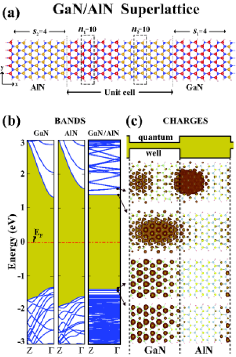
The highest valence band and the lowest conduction band states are flat and they are identified as confined states. As a result, one can deduce a type-I (normal) band alignment since states are confined to the GaN part of heterostructure. One notes that the bandgap of the superlattice in momentum space is different from those of constituent nanoribbons and can also expect that the superlattice band gap in momentum space gets larger as the extension of GaN and AlN sides increases. Similar confined states can be obtained by constructing AlN core and GaN shell structures, where electrons are expected to be confined in the core region.
VII Discussions and conclusions
In view of the exceptional electronic, magnetic and mechanical properties of recently synthesized graphene, questions have been raised whether well-known materials in micro and optoelectronic industry can attain similar honeycomb structures. It is hoped that unusual properties can be attained from these structures. The present paper examined a large number of materials, Group IV elements, binary compounds of these elements, as well as a large number of Group III-V compounds to reveal whether they may form 2D honeycomb structure. For several decades the bulk crystals of these materials have dominated micro and optoelectronic industry. Based on ab-initio structure optimization and calculations of phonon modes we are able to determine 22 honeycomb structure, which can be stable in a local minimum on the Born-Oppenheimer surface as either 2D infinite periodic crystals or finite size flakes (patches). Our calculations reveal that Group IV elements, Si and Ge, and binary compounds SiC, GeC, SnC, SnSi, SnGe and SiGe have stable honeycomb structures. However, while SiC, GeC, SnC are planar like graphene and BN, Si, Ge, SnSi, SnGe and SiGe are buckled (or puckered) for stabilization. We also find that all III-V compounds containing first row elements B, C or N have planar stable structures. However, the binary compounds formed from the combination of Al, Ga, In and P, As, Sb are found to be stable in low buckled structure.
For honeycomb structures which were deduced to stable, an extensive analysis have been carried out to determine their atomic structure, elastic and electronic properties. While Si and Ge are semimetallic and linear band crossing at the Fermi level like graphene, all the binary compounds are found to be semiconductors. Interestingly, these honeycomb materials exhibit interesting trends regarding cohesive energy, band gap, effective charge, in-plane stiffness, Poisson’s ratio depending on the row numbers of their constituent elements or their radius. Interestingly, we deduced a relation between in-plane stiffness and cohesive energy among all honeycomb structures studied in this work.
These materials in honeycomb structure have a variety of band gaps. Even more remarkable is that the nanoribbon forms of these materials provide diverse properties depending on not only their constituents, but also their chirality and width. All these properties are expected to offer number of applications. Therefore, the studies related with their functionalization by vacancy defects or adatoms, their mechanical and spintronic properties, their heterostructures and core-shell structures will open a new field of research. We hope that the findings in this work will promote the research aiming at the synthesis of these materials.
Acknowledgements.
Computing resources used in this work were provided by the National Center for High Performance Computing of Turkey (UYBHM) under grant number 2-024-2007. This work was partially supported by TÜBITAK under grant no: 106T597. S. C and R. T. S acknowledge financial support from TÜBA (Turkish Academy of Sciences).References
- (1) K. S. Novoselov, A. K. Geim, S. V. Morozov,D. Jiang, Y. Zhang, S. V. Dubonos, I. V. Grigorieva, A. A. Firsov, Science 306, 666 (2004).
- (2) P. R. Wallace, Phys. Rev. 71, 622 (1947).
- (3) M. I. Katsnelson, K. S. Novoselov, and A. K. Geim, Nat. Phys. 2, 620 (2006).
- (4) K. S. Novoselov, A. K. Geim, S. V. Morozov, D. Jiang, M. I. Katsnelson, I. V. Grigorieva, S. V. Dubonos, and A. A. Firsov, Nature (London) 438, 197 (2005).
- (5) C. Itzykson and J.-B. Zuber, Quantum Field Theory (Dover, New York) (2006).
- (6) A. Calogeracos and N. Dombey, Contemp. Phys. 40, 313 (1999).
- (7) C. Berger, Z. Song, T. Li, X. Li, A. Y.Ogbazghi, R. Feng, Z. Dai, A. N. Marchenkov, E. H. Conrad, P. N. First, and W. A. de Heer, Science 312, 1191 (2006).
- (8) Y. Zhang, Yan-Wen Tan, H. L. Stormer, and P. Kim, Nature (London) 438, 201 (2005).
- (9) N. D. Mermin, Phys. Rev. 176, 250-254 (1968).
- (10) P. L. Doussal, L. Radzihovsky, Phys. Rev. Lett. 69, 1209 (1992).
- (11) A. Fasolino, J. H. Los and M. I. Katsnelson, Nature Materials (London) 6, 858 (2007).
- (12) J. C. Meyer, A.K Geim, M.I Katsnelson, Nature 446, 60-63 (2007).
- (13) Y. W. Son, M. L. Cohen, and S. G. Louie, Phys. Rev. Lett. 97, 216803 (2006).
- (14) V. Barone, O. Hod, and G. E. Scuseria, Nano Lett. 6, 2748 (2006).
- (15) K. I. Sasaki, S. Murakami, and R. Saito, J. Phys. Soc. Jpn. 75, 074713 (2006).
- (16) D. A. Abanin, P. A. Lee, and L. S. Levitov, Phys. Rev. Lett. 96, 176803 (2006).
- (17) D. A. Areshkin, D. Gunlycke, and C. T. White, Nano Lett. 7, 204 (2007).
- (18) M. Ezawa, Phys. Rev. B 73, 045432 (2007).
- (19) K. Kobayashi, Phys. Rev. B 48, 1757 (1993).
- (20) M. Fujita, K. Wakabayashi, K. Nakada, and K. Kusakabe, J. Phys. Soc. Jap. 65, 1920 (1996).
- (21) K. Nakada, M. Fujita, G. Dresselhaus, and M. S. Dresselhaus, Phys. Rev. B 54, 17954 (1996).
- (22) K. Wakabayashi, M. Sigrist, and M. Fujita, J. Phys. Soc. Jap. 67, 2089 (1998).
- (23) Y.-W. Son, M.L. Cohen and S.G. Louie, Nature 444, 342-347 (2006).
- (24) M. Topsakal, H. Sevinçli, S. Ciraci, Appl. Phys. Lett. 92, 173118 (2008); H. Sevincli, M. Topsakal and S. Ciraci, Phys. Rev. B., 78, 245402 (2008).
- (25) H. Şahin and R. T. Senger, Phys. Rev. B 78, 205423 (2008).
- (26) J.Y. Yan, P. Zhang, B. Sun, H.-Z. Lu, Z. Wang, S. Duan, and X.-G. Zhao, Phys. Rev. B 79, 115403 (2009).
- (27) K. S. Novoselov, D. Jiang, F. Schedin, T. Booth , V. V. Khotkevich, S. Morozov, A. K. Geim, Proc. Natl. Acad. Sci. U.S.A. 102, 10451 (2005)
- (28) D. Pacilé, J. C. Meyer, Ç. Ö. Girit, and A. Zettl, Appl. Phys. Lett. 92, 133107 (2008).
- (29) Z. Zhang and W. Guo, Phys. Rev. B 77, 075403 (2008).
- (30) Cheol-Hwan Park and Steven G. Louie, Nano Lett. 8, 2200 (2008).
- (31) V. Barone, J. E. Peralta, Nano Lett. 8, 2210 (2008).
- (32) M. Topsakal, E. Akturk, and S. Ciraci, Phys. Rev. B 79, 115442 (2009).
- (33) Y. Wang, X. Fan, J. Sun, Materials Letters 63, 350 (2006).
- (34) Y. Huang , J. He, Y. Zhang , Y. Dai , Y. Gu , S. Wang , C. Zou, J. Mater. Sci. 41, 3057-3062 (2006).
- (35) J. Duan, Xintang Huang , E. Wang, Materials Letters 60 1918-1921 (2005).
- (36) G.S Wu , T. Xie , X.Y Yuan, Y.Li , L. Yang , Y.H Xiao, L.D Zhang, Solid State Communications 134, 485-489 (2005).
- (37) M. Topsakal, S. Cahangirov, E. Bekaroglu, arXiv:0907.3070v1.
- (38) C. Tusche, H.L. Meyerheim and J. Kirschner, Phys. Rev. Lett. 99, 026102 (2007).
- (39) A. R. Botello-Mendez, F. Lopez-Urias, M. Terrones, H. Terrones, Nano Letters 6, 1562 (2008).
- (40) A.R. Botello-Mendez, M.T. Martinez-Martinez, F. Lopez-Urias,M. Terrones , H. Terrones, Chem. Phys. Lett. 448, 258 (2007).
- (41) L. Sun , Y. Li , Z. Li , Q. Li , Z.Zhou, Z. Chen , J. Yang ,and J.G. Hou, The J. of Chem. Phys. 17, 174114 (2008).
- (42) E. Bekaroglu, M.Topsakal, S. Changirov and S. Ciraci, to be submitted (2009).
- (43) S. Cahangirov, M. Topsakal, E. Akturk, H. Şahin and S. Ciraci, Phys. Rev. Lett. 102, 236804 (2009).
- (44) K. Takeda and K. Shiraishi, Phys. Rev. B 50, 14916 (1994).
- (45) E. Durgun, S. Tongay and S. Ciraci, Phys. Rev. B 72, 075420 (2005).
- (46) H. Nakano, T. Mitsuoka, M. Harada, K. Horibuchi, H. Nozaki, N. Takahashi, T. Nonaka, Y. Seno, H. Nakamura, Angew Chem. 118, 6451 (2006).
- (47) R. Krishnan, Q. Xie, J. Kulik, X. D. Wang, S. Lu, M. Molinari, Y. Gao, T. D. Krauss, P. M. Fauchet, J. of Appl. Phys. 96, 1 (2004).
- (48) G. Kresse, J. Hafner, Phys. Rev. B 47, 558 (1993).
- (49) G. Kresse, J. Furthmüller, Phys. Rev. B 54, 11169 (1996).
- (50) P. E. Blochl, Phys. Rev. B 50, 17953 (1994).
- (51) D. M. Ceperley and B.J. Alder, Phys. Rev. Lett. 45, 566 (1980).
- (52) M. Shishkin, G. Kresse, Phys. Rev B 74, 035101 (2006).
- (53) G. Henkelman, A. Arnaldsson, H. Jonsson, Comput. Mater. Sci.36, 254-360 (2006).
- (54) D. Alfè, Comp. Phys. Comm., doi:10.1016/ j.cpc.2009.03.010 (2009).
- (55) P. G. Klemens, Int. J. Thermophysics 22, 265 (2001).
- (56) I. H. Lee and R. M. Martin, Phys. Rev. B 56, 7197 (1997).
- (57) S. Narasimhan and S. de Gironcoli, Phys. Rev. B 65, 064302 (2002).
- (58) Jia-An Yan, W. Y. Ruan, and M. Y. Chou, Phys. Rev. B 77, 125401 (2008).
- (59) S. Piscanec, M. Lazzeri, F. Mauri, A. C. Ferrari, and J. Robertson, Phys. Rev. Lett. 93, 185503 (2004).
- (60) J. O. Sofo, A. S. Chaudhari and G. D. Barber, Phys. Rev. B 75, 153401 (2007).
- (61) D. C. Elias, R. R. Nair, T. M. G. Mohiuddin, S. V. Morozov, P. Blake, M. P. Halsall, A. C. Ferrari, D. W. Boukhvalov, M. I. Katsnelson, A. K. Geim, K. S. Novoselov, Science 323, 610 (2009).
- (62) H. Şahin, C. Ataca and S. Ciraci, arXiv:0907.0549v1
- (63) H. A. Jahn, E. Teller, Proc. R. Soc. London A 161, 220 (1937).
- (64) B. Meyer, Adv. Inorg. Radiochem. 18, 297 (1976).
- (65) B. Webster, Chemical Bonding Theory (Blackwell, Oxford, 1990).
- (66) J. F. Labarre, Struct. Bonding 35, 1 (1978).
- (67) R. Hazenkampf, T. Migchelsen and A. Vos, Acta Crystallog. 15, 539 (1962).
- (68) J. F. Nye, Physical Properties of Crystals (Clarendon Press, Oxford, 1985).
- (69) C. Lee, X. Wei, J. W. Kysar, J. Hone, Science 321, 385 (2008).
- (70) X. Wang, Y. Ouyang, X. Li, H. Wang, J. Guo, H. Dai, Phys. Rev. Lett. 100, 206803 (2008).
- (71) A. K. Geim and K. S. Novoselov, Nature Mater. 6, 183 (2007).
- (72) A. H. Castro Neto, F. Guinea, N. M. R. Peres, K. S. Novoselov and A. K. Geim, Rev. Mod. Phys. 81, 109 (2009).
- (73) W. A. Harrison, Electronic Structure and Properties of Solids-The Physics of Chemical Bonds (Freeman, San Francisco, 1980).
- (74) E. Durgun, S. Dag, O. Gulseren and S. Ciraci, J. of Phys. Chem. B,108, 575 (2004).; H. Sevincli, M. Topsakal, E. Durgun and S. Ciraci, Phys. Rev. B., 77, 195434 (2008).