Low-Temperature Resistivity Anomalies in Periodic Curved Surfaces
Abstract
Effects of periodic curvature on the the electrical resistivity of corrugated semiconductor films are theoretically considered. The presence of a curvature-induced potential affects the motion of electrons confined to the thin curved film, resulting in a significant resistivity enhancement at specific values of two geometric parameters: the amplitude and period of the surface corrugation. The maximal values of the two parameters in order to observe the corrugation-induced resistivity enhancement in actual experiments are quantified by employing existing material constants.
keywords:
surface curvature, electron-electron umklapp scattering, low-temperature resistivity1 Introduction
Geometric curvature of nano-scale conducting films with curved geometry[1, 2, 3] provides us a clue to synthesize a new class of quantum devices based on curved nanomaterials. The most relevant nature is the occurrence of a curvature-dependent potential (CP) that acts on low-energy electrons moving in the curved systems[4, 5, 6, 7, 8]. The mechanism of the CP have been considered from various perspectives[9, 10, 11, 12, 13, 14, 15, 16], which triggered interesting theoretical predictions on the electric transport properties of curved nanostructures: quantum transmission probabilities in Y-nanojunction[17], a charge separation in helicoidal ribbons[18], and an anomalous shift of the Tomonaga-Luttinger exponent in deformed nanocylinders[19, 20] are only a few to mention.
In the earlier work, the authors have studied the CP effect on the electrical resistivity of corrugated semiconductor films[21]. A specific magnitude of the corrugation amplitude turned out to cause a significant increase in the resistivity, which is due to the CP-enhanced population of the electron-electron umklapp scattering processes relevant to the resistivity. This result motivates us to complete a thorough check of the CP effect in a wider range of two geometric parameters, i.e., the corrugation amplitude and period, that determine the shape of the corrugated film. This attempt is crucially important in order to make use of the effect in developing curved-nanomaterial-based quantum devices.
In this paper, we analyze systematically the correlation between the two geometric parameters and the CP-induced resistivity enhancement of the corrugated semiconductor films. We show that the degree of contributions from electron-electron scatterings to the resistivity is strongly dependent on the values of the two parameters. The present results enable to determine the maximal surface geometry that is requisite for the resistivity enhancement to get sizable in actual experiments.
2 Gap formation by periodic curvature
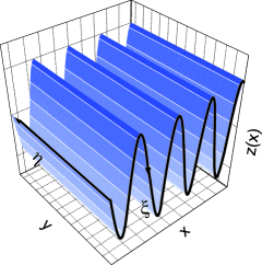
Let us consider a two dimensional (2D) electron system confined to a thin film, in which the film is subjected to an unidirectional corrugation along the axis. The height of the film in the direction is given by
| (1) |
where and are the amplitude and period of corrugation, respectively (see Fig. 1). By transforming the variables into
| (2) |
with the definition , we obtain the Schrödinger equation [21]
| (3) |
Here, the potential is the CP associated with the periodic corrugation,
| (4) |
and is the effective mass of conducting electrons. Equation (3) is solved by using the Fourier series expansion
| (5) |
as a result of which the energy-band structure with respect to the wavevector is obtained.
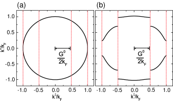
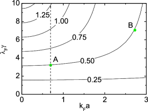
The periodic nature of with the period implies an occurrence of gaps at ( is a positive integer) in the Fermi circle, where defines the reciprocal lattice vector associated with the periodicity of . Such gaps are observed in Fig. 2(b), where a sufficiently large amplitude of is assumed by setting appropriate values of and . Still, it should be noted that gaps at may and may not occur once is given. This is primary because as well as are two-variable functions of and as understood from Fig. 1. Hence, different pairs of the two values can yield the same value of , though the pairs do not always produce a gap at .
Two contrast examples of the Fermi circle are clearly demonstrated in Figs. 2(a) and 2(b). We set and to draw the Fermi circles, in which both pairs give an identical value of as shown in the contour plot of in Fig. 3; the points and in the plot correspond to Fig. 2(a) and 2(b), respectively. The Fermi circle in Fig.2(a) has almost no gap, whereas that in Fig.2(b) shows clear gaps at and . As we shall see later, usage of such pairs that lead to gaps in the Fermi circle is a necessary condition for the corrugation-induced jump in the resistivity to be observed.
3 Resistivity of the corrugated film
We now consider the low-temperature resistivity of 2D electron systems under periodic modulation. Contributions of two-electron scatterings to the resistivity at low temperature are expressed by[21, 22]
| (6) |
where are the Boltzmann constant and the Fermi energy, respectively. represent the contributions from the th umklapp scatterings that satisfy the momentum conservation law:
| (7) |
is satisfied because of the inversion symmetry of the Fermi circle with respect to . Equation (6) holds for , i.e., when smearing of the Fermi degeneracy by thermal fluctuation can be negligible so that electron-electron scatterings are allowed just on the Fermi circle.
Each in Eq. (6) sums up contributions from all possible th-order processes that satisfy Eq. (7). Among many processes, specific ones involving the state that locates near the gap are dominant in the total value of [21]. Furthermore, the number of such dominant processes takes the maximum when gaps open at both ends of the Fermi circle (), i.e., when the relation
| (8) |
is satisfied. As a result, the surface corrugation with and that satisfy Eq. (8) can cause the corrugation-induced jump in . We emphasize again that Eq. (8) is a necessary (not sufficient) condition of the jump in , since gaps may and may not be present for a given .
4 Numerical Results
In numerical calculations of , we set meV and employed material constants of the GaAs/AlxGa1-xAs heterostructures: the effective mass is =0.067 ( is a bare electron mass) and the dielectric constant is =13.2 ( is the dielectric constant of vacuum).
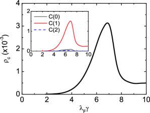
Figure 4 shows the dependence of ; we fixed =0.7 and increased from to as indicated by the dotted trajectory in Fig. 3. has a peak at under the condition of , which is a consequence of the satisfied relation as seen from Fig. 3. Hence, the peak of at 7.0 tells us that the pair of the above mentioned values generates gaps at in the Fermi circle. In the inset of Fig. 4, we also show the dependences of with , 1 and . The term is found to be dominant at all values of , which imply that overall behavior of in the region considered is determined by the first-order umklapp process.
5 Discussions
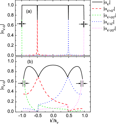
We discuss the reason why the contributions from the second umklapp processes do not enhance at in Fig. 4. Figures 5(a) and 5(b) show the profiles of the Fourier coefficients (see Eq. (5)) under the numerical conditions of and marked in Fig. 3, respectively. In both figures, upward peaks of with touch downward peaks of at . The widths of the upward peaks are estimated as [23]
| (9) |
where is the Fourier component of the CP. We can deduce from Eq. (9) that for and for ; furthermore, it follows from Eq. (9) that increases monotonically with increasing and . Notice that the larger width results in the larger , since the number of the associated umklapp processes increase. In fact, is needed to get under the condition that yields 1 or 2. (The magnitude of is large enough to observe it experimentally[24].) These arguments account for the reason why the parameters corresponding to , which provide , give no peak in in Fig. 4.
We have also confirmed that for and for are enough to yield , where is assumed. Our results reveal the geometric conditions of the surface corrugation to obtain a sizable jump in of a semiconductor film. The same approach is applicable to other semiconducting materials than the GaAs/AlxGa1-xAs heterostructures we have considered.
6 Conclusion
In conclusion, we have demonstrated the curvature-induced enhancement of of periodically curved thin films at low . Appropriate values of and for the resistivity enhancement to appear in measurements have been clarified using existing material constants. The umklapp contributions to the resistivity have been found to increase significantly when the value of and satisfy the conditions given by and . We hope that experimental tests of our theoretical predictions open a gate for next-generation devices based on curved nanostructures.
Acknowledgments
We would like to thank K. Yakubo, S. Nishino, H. Suzuura, and S. Uryu for useful discussions and suggestions. This study was supported by a Grant-in-Aid for Scientific Research from the MEXT, Japan. H.S. is thankful for the financial support from Executive Office of Research Strategy in Hokkaido University. A part of numerical simulations were carried out using the facilities of the Supercomputer Center, ISSP, University of Tokyo.
References
- [1] V. Ya. Prinz, D. Grützmacher, A. Beyer, C. David, B. Ketterer and E. Deckardt, Nanotechnology 12, 399 (2001).
- [2] A. Lorke, S. Bohm and W. Wegscheider, Superlattices Microstruct. 33, 347 (2003).
- [3] V. Ya. Prinz, Phys. Status. Solidi B 243, 3333 (2006).
- [4] H. Jensen and H. Koppe, Ann. Phys. 63, 586 (1971).
- [5] R. C. T. da Costa, Phys. Rev. A 23, 1982 (1981).
- [6] M. Ikegami and Y. Nagaoka, Prog. Theor. Phys. , 253 (1991).
- [7] L. Kaplan, N. T. Maitra and E. J. Heller, Phys. Rev. A 56, 2592 (1997).
- [8] P. C. Schuster and R. L. Jaffe, Ann. Phys. 307, 132 (2003).
- [9] G. Cantele, D. Ninno and G. Iadonisi, Phys. Rev. B 61, 13730 (2000).
- [10] M. V. Entin and L.I. Magarill, Phys. Rev. B , 085330 (2001).
- [11] H. Aoki, M. Koshino, D. Takeda, and H. Morise, Rhys. Rev. B , 035102 (2001).
- [12] N. Fujita, J. Phys. Soc. Jpn. , 3115 (2004).
- [13] J. Gravesen and M. Willatzen, Phys. Rev. A 72, 032108 (2005).
- [14] A. Marchi, S. Reggiani, M. Rudan and A. Bertoni, Phys. Rev. B 72, 035403 (2005).
- [15] M. Encinosa, Phys. Rev. A 73, 012102 (2006).
- [16] G. Ferrari and G. Cuoghi, Phys. Rev. Lett. 100, 230403 (2008).
- [17] G. Cuoghi, G. Ferrari and A. Bertoni, Phys. Rev. B 79, 073410 (2009).
- [18] V. Atanasov and R. Dandoloff and A. Saxena, Phys. Rev. B 79, 033404 (2009).
- [19] H. Shima, H. Yoshioka, and J. Onoe, Phys. Rev. B , 201401(R) (2009).
- [20] H. Shima, H. Yoshioka, and J. Onoe, arXiv: 0908.2565.
- [21] S. Ono and H. Shima, Phys. Rev. B , 235407 (2009).
- [22] S. Uryu and T. Ando, Phys. Rev. B 64, 195334 (2001).
- [23] C. Kittel, Introduction to Solid State Physics (John Wiley and Sons, Inc., New York, Seventh Edition, 1996).
- [24] A. Messica, A. Soibel, U. Meirav, A. Stern, H. Shtrikman, V. Umansky, and D. Mahalu, Phys. Rev. Lett , 705 (1997).