Structure and energetics of Si(111)-(52)-Au
Abstract
We propose a new structural model for the Si(111)-(52)-Au reconstruction. The model incorporates a new experimental value of 0.6 monolayer for the coverage of gold atoms, equivalent to six gold atoms per 52 cell. Five main theoretical results, obtained from first-principles total-energy calculations, support the model. (1) In the presence of silicon adatoms the periodicity of the gold rows spontaneously doubles, in agreement with experiment. (2) The dependence of the surface energy on the adatom coverage indicates that a uniformly covered phase is unstable and will phase-separate into empty and covered regions, as observed experimentally. (3) Theoretical scanning tunneling microscopy images are in excellent agreement with experiment. (4) The calculated band structure is consistent with angle-resolved photoemission spectra; analysis of their correspondence allows the straightforward assignment of observed surface states to specific atoms. (5) The calculated activation barrier for diffusion of silicon adatoms along the row direction is in excellent agreement with the experimentally measured barrier.
pacs:
68.43.Bc,73.20.At,68.37.Ef,68.43.JkI Introduction
Forty years ago Bishop and Riviere first observed the (111) surface of silicon to reconstruct, with fivefold periodicity, in the presence of gold. bishop_j_phys_d_appl_physics_1969a Since that time the Si(111)-(52)-Au reconstruction has been widely studied, in several hundred publications, as a prototype linear metallic chain system in which the physics of one-dimensional metals is approximately realized.hasegawa_j_phys_condens_matter_2000a ; matsuda_j_phys_condens_matter_2007a
These investigations have provided very substantial insights into many aspects of Si(111)-(52)-Au.barke_solid_state_comm_2007a ; barke_appl_surf_sci_2007a Less successful have been the many attempts to use the clues provided by experiment to construct a complete structural model for this complicated reconstruction. Beginning with the early work of LeLay over a dozen different models have been proposed.lelay_surf_sci_1977a ; berman_phys_rev_b_1988a ; hasegawa_journal_of_vacuum_science__technology_a_1990a ; bauer_surf_sci_1991a ; schamper_phys_rev_b_1991a ; seehofer_surf_sci_1995a ; marks_phys_rev_lett_1995a ; plass_surf_sci_1997a ; omahony_phys_rev_b_1994a ; omahony_surf_sci_1992a ; shibata_phys_rev_b_1998b ; hasegawa_surf_sci_1996a ; hasegawa_phys_rev_b_1996a ; hasegawa_surf_sci_1996b ; erwin_phys_rev_lett_2003a ; kang_surf_sci_2003a ; riikonen_phys_rev_b_2005a ; ren_phys_rev_b_2007a ; chuang_phys_rev_b_2008a All were eventually found to be inconsistent with the results of scanning tunneling microscopy (STM), angle-resolved photoemission spectroscopy (ARPES), or both.
In this paper we propose a new structural model for Si(111)-(52)-Au that is fully consistent with all experimental data to which we have compared. The model is similar to one proposed by Erwin in 2003,erwin_phys_rev_lett_2003a but is modified to be consistent with a recently revised value of the gold coverage.barke:155301 The modifications, although seemingly minor, for the first time bring the predictions of the model—for STM and ARPES as well as other phenomena—into excellent agreement with experiment. More importantly, the new model opens the door to a more fundamental physical understanding of Si(111)-(52)-Au based on its detailed atomic structure.
II Structural model
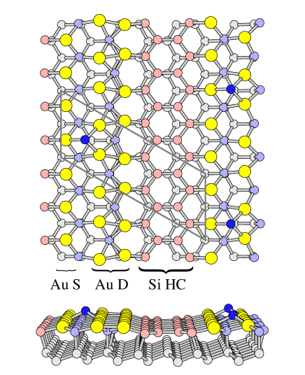
The model proposed here is shown in Fig. 1. The basic structure is similar to one proposed several years ago in Ref. erwin_phys_rev_lett_2003a, but there are several important differences. For this reason it is useful to discuss both the similarities and differences between the older model and the one proposed here (hereafter the “2003 model” and the “2009 model”).
The starting point for the 2003 model was the experimental observation that 0.4 monolayer (ML) of gold induces a stable reconstruction of the Si(111) surface. Using this coverage value the 2003 model was constructed with four gold atoms per 52 cell. As shown in Fig. 1 of Ref. erwin_phys_rev_lett_2003a, , the gold atoms substitute for silicon atoms in the topmost surface layer, forming two Au-Si chains oriented along the [10] direction. Adjacent to these two chains is a silicon “honeycomb chain,” a thin graphitic strip of silicon that owes its stability to a Si=Si double bond. The basic reconstruction just described has 51 periodicity. The experimentally observed 52 substrate periodicity was argued to arise from a row of silicon rebonding atoms that bridges a channel between one of the Au-Si rows and the silicon honeycomb chain. A full row of rebonding atoms overcoordinates some atoms, while a half-occupied row, with 52 periodicity, leaves some dangling bonds unsaturated. The latter arrangement was argued to be energetically preferred when the system is doped with extra electrons. These were supplied by silicon adatoms adsorbed on top of the Au-Si chains.
The recently revised experimental determination of the gold coverage as 0.6 ML obviously calls for a revised structural model as well.barke:155301 The 2009 model accommodates the additional two gold atoms per 52 cell by replacing the half-occupied rebonding row of silicon atoms from the 2003 model with a full row of gold atoms. The other two building blocks of the 2003 model—the silicon honeycomb chain and the adsorbed silicon adatoms—are unchanged in the new model. The total coverage of silicon atoms in the top layer of the 2009 model varies, according to the coverage of adatoms, between 1.20 ML (for the undecorated surface) and 1.25 ML (for saturation coverage). These values are consistent with the range of experimentally determined silicon coverage, 1.1 to 1.3 ML (Ref. tanishiro1990a, ), 1.230.003 ML (Ref. seifert_dissertation_2006a, ), and 1.30.1 ML (Ref. chin2007a, ). The 2009 model is energetically more favorable than the 2003 model: the theoretical surface energy is 17.1 meV/Å2 lower in the Au-rich limit, in which the chemical potential is taken as the bulk energy per atom.chempotAu
Much of the rest of this paper will focus on the interesting role played by the new row of gold atoms. But it is worth pausing briefly to place Si(111)-(52)-Au in the larger context of other metal-induced reconstructions of Si(111). It is now known that a great variety of metal adsorbates induce closely related reconstructions based on the silicon honeycomb chain. But the details differ, sometimes with unexpected consequences. Easily ionized adsorbates such as alkalis, alkaline earths, and some rare earths form a family of “honeycomb-chain channel” (HCC) reconstructions in which the adsorbates occupy channels between adjacent silicon honeycomb chains.collazo-davila_phys_rev_lett_1998a ; lottermoser_phys_rev_lett_1998a ; erwin_phys_rev_lett_1998a Each adsorbate is three-fold coordinated by silicon atoms in the honeycomb chain, which are too far away (3.0 Å) to form covalent bonds, consistent with a picture of ionic charge donation and electrostatic attraction. The interactions between adsorbates are also electrostatic, but repulsive.erwin_surf_sci_2005a Within this family of HCC reconstructions the adsorbate coverage is determined by a simple electron-counting rule first proposed by Lee et al.lee2001a ; lee2003a and later generalized by Battaglia et al.battaglia2007a ; battaglia:075409
Adsorbates that are less ionic, such as silver and gold, also form reconstructions based on the silicon honeycomb chain but the role of the adsorbate is more interesting. Silver adsorbates occupy the channel of a HCC-like reconstruction,collazo-davila_phys_rev_lett_1998a but the stronger interaction between silver and silicon leads to a preference for two-fold coordination of silver by silicon, at a much reduced distance of 2.6 Å. The two-fold coordination brings silver adsorbates sufficiently close to each other to allow pairing into silver dimers. Chuang et al.chuang2008a and Urbieta et al.urbieta2009a showed that the phase of this pairing alternates between adjacent channels, modulating the periodicity of the basic 31 HCC reconstruction to a variant.
Returning now to Si(111)-(52)-Au, it appears that the role of the adsorbate is still more complex. Gold is very reactive on silicon surfaces.doremus2001a This reactivity is already evident in the Au-Si rows of Fig. 1. Within these rows gold completely substitutes for the top layer of the surface silicon bilayer, with each gold atom covalently bonded to three silicon atoms. Likewise, each silicon atom at the edge of the silicon honeycomb chain forms a covalent bond to a gold atom. The Au-Si bond lengths, both within the Au-Si rows and bonded to the silicon honeycomb chain, are 2.5 Å, smaller than for any other adsorbate studied.
The most interesting aspect of the 2009 model is the behavior of the gold double row labeled “Au D” in Fig. 1. As shown in the figure, the equilibrium geometry of this double row is dimerized. Period doubling was also part of the 2003 model, but its origin—the half-occupied rebonding row—was simpler. In the 2009 model the dimerization occurs only in the presence of silicon adatoms, or when the surface is doped with extra electrons. In Sec. IV we show that these two scenarios are largely equivalent. We further demonstrate that in the presence of adatoms the dimerization is driven by an unusual “double” Peierls mechanism, in which the distortion opens two gaps in the band structure of the undistorted 51 substrate.
III Methods
III.1 Theoretical methods
First-principles total-energy calculations were used to determine equilibrium geometries and relative energies of the basic model and its variants. The calculations were performed in a slab geometry with four layers of Si plus the reconstructed top surface layer and a vacuum region of 8 Å. All atomic positions were relaxed, except the bottom Si layer and its passivating hydrogen layer, until the largest force component on every atom was below 0.01 eV/Å. Total energies and forces were calculated within the PBE generalized-gradient approximation to density-functional theory (DFT) using projector-augmented-wave potentials, as implemented in vasp. kresse_phys_rev_b_1993a ; kresse_phys_rev_b_1996a The plane-wave cutoff for all calculations was 250 eV.
The sampling of the surface Brillouin zone was chosen according to the size of the surface unit cell and the relevant precision requirements. For example, the dependence of the total energy on dimerization (Fig. 2) was calculated using a 54 unit cell and 22 zone sampling, with convergence checks using 44 sampling. The dependence of the relative surface energy on silicon adatom coverage (Fig. 3) requires greater precision because the energy variations are smaller. Hence these surface energies were calculated using a 58 unit cell (to allow an adatom coverage of 1/8) and 84 sampling, with convergence checks using 126 sampling. Finally, the potential-energy surface for adatom diffusion (Fig. 7) was calculated using a 54 unit cell and 22 zone sampling.
Simulated STM images (Fig. 4) were calculated using the method of Tersoff and Hamann.tersoff_phys_rev_b_1985a For the filled-state image we integrated the local density of states (LDOS) over a chosen energy window of occupied states up to the Fermi level; for the empty-state image the integration was over unoccupied states starting at the Fermi level. The simulated STM topography under constant-current conditions was obtained by plotting the height at which the integrated LDOS is constant.
III.2 Experimental methods
Silicon wafers (from Virginia Semiconductors) were degassed for several hours at 700 ∘C before flashing at 1250 ∘C for a few seconds. A rapid cool-down to 850 ∘C was followed by slow cooling to room temperature. An important prerequisite for obtaining well-defined row structures was a flexible mount of the samples that prevented strain from building up during high-temperature flashing. Gold was evaporated from a Mo wire basket. The pressure was kept below 510−10 mbar throughout the sample preparation. All STM measurements were carried out at room temperature with low tunneling currents (50 pA).
Band dispersions were obtained using a Scienta 200 spectrometer with multidetection and an energy resolution of 20 meV for electrons and 7 meV for photons. We used -polarized synchrotron radiation at a photon energy = 34 eV, where the cross section of silicon surface states has a maximum relative to the bulk states. The data are for a sample temperature below 100 K.
IV Energetics
This section addresses three issues related to the energetics of Si(111)-(52)-Au. We consider first the energetics of dimerization, and show that dimerization occurs naturally within the 2009 model when silicon adatoms or extra electrons are present. Next we examine how the surface energy varies as a function of silicon adatom coverage; we find that the energy is minimized for the coverage 1/4 shown in Fig. 1. Finally, we show that the model explains the existence of a localized defect structure seen even on carefully prepared surfaces.
IV.1 Dimerization of the substrate
The model shown in Fig. 1 has 54 periodicity, because silicon adatoms decorate the surface in a 54 arrangement. But it is clear from the figure that the underlying substrate (that is, ignoring the adatoms) can be understood more simply as a 51 reconstruction whose periodicity is doubled, along the chain direction, to 52 by dimerization within the Au double row. Understanding the nature and origin of this dimerization is important for explaining many experimental aspects of Si(111)-(52)-Au, including the fine details of STM imagery, data from ARPES, the observation of nanoscale phase separation,kirakosian_surf_sci_2003a ; kirakosian_phys_rev_b_2003a ; mcchesney_phys_rev_b_2004a ; yoon_phys_rev_b_2005a ; choi_phys_rev_lett_2008a the diffusion of silicon adatoms on the surface,hasegawa_phys_rev_b_1996a ; bussmann_phys_rev_lett_2008a and the existence and motion of domain walls within the Au-Si rows.kang_phys_rev_lett_2008a
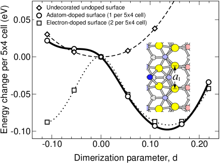
We begin by defining more precisely the nature of the dimerization. The inset to Fig. 2 shows a detail of the gold double row near a silicon adatom. Within this double row the gold atoms have a ladder-like arrangement, with Au-Au bonds as the rungs. In the absence of adatoms (or extra electrons) these rungs are all parallel to each other, with a spacing equal to the silicon surface lattice constant . When adatoms decorate the surface in the 54 arrangement shown in Fig. 1 the rungs rotate away from their parallel alignment. This rotation occurs almost completely within the (111) surface plane, and the rungs are quite rigid: the Au-Au bond length (2.94 Å) changes by less than 1%. This rigidity is not surprising, because the Au-Au bond length is already very close to the bulk gold bond length (2.88 Å). The sign of the rotation alternates along the chain direction. Hence the dimerization can be viewed as an antiferrodistortive instability.
To quantify the dimerization one could, of course, use the angle of rotation of the Au-Au rungs. We choose instead a more physically transparent measure: the distance between gold atoms on the side of the double row adjacent to the silicon honeycomb chain, as labeled in Fig. 2. A dimensionless dimerization parameter can then be defined, . For the 54 arrangement of adatoms shown in Fig. 1, the equilibrium dimerization parameter is .
Some insight into the origin of the dimerization may be obtained by computing the DFT total energy as a function of while relaxing all other degrees of freedom. The results are shown in Fig. 2 for three variants of the basic model: the undecorated and undoped surface (without adatoms or extra electrons); the adatom-doped 54 surface of Fig. 1; and the undecorated surface doped with two extra electrons per 54 cell. For the undecorated undoped surface the minimum is at , indicating that dimerization is not stable. For the adatom-doped surface there is a single minimum in the energy, as expected, at . For the electron-doped surface the behavior of is nearly indistinguishable, for positive , from that of the adatom-doped surface. This similarity strongly suggests that each silicon adatom dopes two electrons to surface states. More substantive evidence for this conjecture is found in the electronic structure of these variants, as we show below in Sec. VI.
The behavior of for negative , however, is very different. This is because adatom-doping strongly breaks the 52 symmetry of the surface, while electron-doping does not. This suggests another role for the silicon adatoms: to pin the phase of the dimerization such that at the position of the adatom. We will return to this role in Sec. VII when considering the diffusion of adatoms.
IV.2 Adatom coverage and phase separation
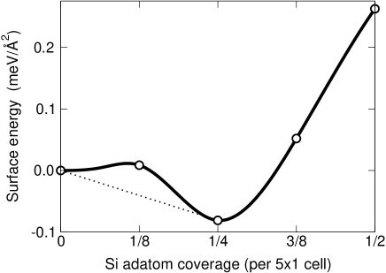
The preceding discussion and calculations were based on the assumption that silicon adatoms decorate the surface in a 54 arrangement, equivalent to a coverage of 1/4 adatom per 51 cell. This phase can be achieved experimentally by depositing silicon onto the surface at temperatures around 300 ∘C until saturation is reached.bennewitz_nanotechnology_2002a But this saturated phase is metastable: annealing causes half of the silicon adatoms to diffuse away. The resulting equilibrium phase is not uniform, but instead exhibits patches with local adatom coverage of 1/4 interspersed with patches of undecorated surface; the global average adatom coverage is close to 1/8.kirakosian_surf_sci_2003a ; kirakosian_phys_rev_b_2003a ; mcchesney_phys_rev_b_2004a ; yoon_phys_rev_b_2005a ; choi_phys_rev_lett_2008a This experimental result poses two questions for theory. (1) What coverage of silicon adatoms minimizes the calculated surface energy? (2) Does the observed patchiness of the adatom distribution arise from an instability toward phase separation?
To compare the energies of phases with different silicon adatom coverage, we compute the relative surface energy
| (1) |
where is the total energy of a surface unit cell containing silicon atoms (including adatoms), and is the silicon chemical potential. Thermodynamic equilibrium between the surface and the bulk requires to be the energy per atom in bulk silicon. Although we do not explicitly consider the free energy at finite temperature, configurational entropy effects may indeed play a role; see below.
Within this formalism, adatoms are thermodynamically stable only if their presence lowers the surface energy of the undecorated surface. Equation 1 shows that this requirement implies that the adsorption energy per adatom must be greater than the silicon cohesive energy (5.4 eV within DFT/PBE). Adsorption energies below this threshold imply that adatoms may be temporarily metastable, but not thermodynamically stable. This is a very stringent requirement, and one that is rarely satisfied in our experience (it was not in the 2003 model).
We calculated the relative surface energies for five different silicon adatom coverages. To minimize numerical uncertainties the same 58 supercell was used for each coverage, and full relaxation performed in every case. The results are shown in Fig. 3. The surface energy is minimized for a coverage of 1/4. This is the coverage depicted in Fig. 1, and agrees well with the experimentally observed local coverage within adatom-covered patches. In Sec. VI we show why the value 1/4 is special: at this adatom coverage—but at no other—the surface band structure is fully gapped and hence favored because occupied states can move down in energy.
We turn now to the second question posed above. Of the five coverages considered here, the second most-favorable is not the adjacent 1/8 or 3/8 phase, but rather the undecorated “empty” surface. In other words, the surface energy of the intermediate 1/8 phase is higher than the average of the two endpoint phases, empty and 1/4. This result suggests that a range of such intermediate coverages between 0 and 1/4 may have energies above the tie line, shown in Fig. 3, connecting the two endpoint phases. This implies that a surface prepared with adatom coverage 1/8 (and perhaps any intermediate coverage between 0 and 1/4) will phase separate into a mixture of empty and 1/4-covered regions.
Of course, this conclusion does not answer the related question of why the observed global average coverage is close to 1/8. We hypothesize that the 1/8 phase may be stabilized at finite temperature by the entropy gained from occupying only half the adatom sites of the 1/4 phase. We also do not address here the characteristic size of the phase-separated regions; this would require analyzing the energy cost of forming the phase boundary between the 0 and 1/4 phases. Finally, we leave for future analysis the possibility that the phase-separated state benefits electrostatically from the charge transfer proposed by Yoon et al. to take place between the 0 and 1/4 phases.yoon_phys_rev_b_2005a
IV.3 Low-energy defect structure
In addition to the phase separation just discussed, STM images of Si(111)-(52)-Au sometimes reveal the presence of an occasional “mirror-domain” defect.yoon_phys_rev_b_2005a ; seifert_dissertation_2006a The signature of this defect is a slight shift, by roughly 3 Å to the right in Fig. 1, of the bright protrusions that dominate the STM topography. The intensity of the protrusions and the position and shape of the underlying features are not affected.
A simple variation of the basic structural model accounts for the observed defects. Starting from the structure shown in Fig. 1, one can construct a mirror-image variant by reflecting the entire top layer of atoms through the vertical plane bisecting the Si=Si double bonds of the honeycomb chain. (This mirror plane was discussed in Ref. erwin_phys_rev_lett_1998a, and is shown in Fig. 1 therein.) The reflection leaves the honeycomb chain unaffected but reverses the ordering and orientation of the Au-Si rows. The geometry of the rigidly reflected structure is already extremely close (within a few hundreths of an Ångstrom) to the fully relaxed geometry. The reflection shifts the silicon adatoms by 2.2 Å to the right, consistent with the observed shift.
The surface energy of the relaxed defect reconstruction is only slightly higher, by 1.2 meV/Å2, than that of the original reconstruction. From inspection of the atomic positions of the original and defect models, we judge the energy cost of forming an interface between the two phases to be quite small. Thus it is plausible that short sequences of this defect structure—manifested as a small rightward shift of the silicon adatoms—should appear even on carefully prepared surfaces, with minimal disruption to either the primary reconstruction or the local adatom coverage.
V Comparison with STM
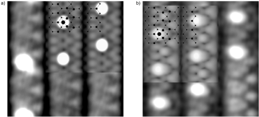
Two decades of studies probing the Si(111)-(52)-Au surface with STM have created a richly detailed and consistent picture of its topography and bias dependence. baski_phys_rev_b_1990a ; omahony_surf_sci_1992a ; omahony_phys_rev_b_1994a ; shibata_phys_rev_b_1998b ; hasegawa_surf_sci_1996a ; hasegawa_phys_rev_b_1996a ; hasegawa_surf_sci_1996b ; hasegawa_journal_of_vacuum_science__technology_a_1990a These data make possible a very stringent test for any proposed structural model by comparing theoretically simulated STM images to atomic-resolution experimental images. In this section we show that simulated images based on the 2009 model are in excellent and detailed agreement with recent experimental images. Moreover, the new model resolves a small but irritating discrepancy found in comparisons based on the earlier 2003 model.
The most pronounced features in STM imagery of the Si(111)-(52)-Au surface are the bright protrusions now well established as originating from the silicon adatoms. In topographic maps these are generally the highest features in both filled- and empty-state images. As discussed elsewhere mcchesney_phys_rev_b_2004a and in the previous section, the adatoms occupy a 54 lattice. Much detailed information is contained in the imagery in between these lattice sites; the topography of this substrate has 52 periodicity. Of special interest is the registry of the 54 adatom lattice and the 52 substrate; the relative alignment of these two lattices provides an important test for structural models. (We do not address here the lack of correlation between the adatoms in different rows, previously discussed in Ref. kirakosian_phys_rev_b_2003a, .)
Figure 4 shows experimental and theoretical simulated STM images for filled and empty states of the Si(111)-(52)-Au surface, in a region where the silicon adatom coverage is 1/4. The agreement between experiment and theory is excellent, and allows all of the main experimental features to be easily identified. (1) The dark vertical channels separating the three main rows shown in Fig. 4 arise from the doubly-bonded rungs of the silicon honeycomb chains. (2) The bright protrusions are from the silicon adatoms. (3) The triangular features with 2 periodicity, constituting the right edge of the rows, arise from the combination of two contributions: a pair of outer gold atoms brought close by dimerization (the apex of the triangle) and two silicon atoms at the left edge of the honeycomb chain (the base of the triangle). (4) In the filled states, the left edge of the rows is not well resolved, and appears to have either 1 or very weak 2 periodicity; these spots arise from the silicon atoms at the right edge of the honeycomb chain. (5) In the empty states, the 2 triangular features on the right edge of the rows alternate with V-shaped features that open to the left. These are a combination of two contributions: a pair of dimerized inner gold atoms (the apex of the V) and Si-Au bonds that are slightly dimerized by their proximity to the gold double row (the arms of the V).
In the experimental images the alignment of the 54 adatom lattice and the 52 substrate topography is as follows. The bright protrusions are located slightly to the left side within the main rows—except in the defect regions discussed in the previous section, where the protrusions are shifted to an equivalent location on the right side of the row. This off-center location is accurately reproduced in the simulated images based on both the original model and the defect model (not shown). Along the rows of the experimental images, the 54 protrusions are symmetrically straddled by the 52 triangular and V-shaped features of the substrate. Fig. 4 shows that this symmetric registry is properly reproduced in the simulated images—resolving a problem with the 2003 model first pointed out by Seifert whereby the alignment of the two lattices was asymmetric.seifert_dissertation_2006a
VI Electronic structure
Photoemission studies of Si(111)-(52)-Au began in the mid-1990s and continue today.collins_surf_sci_1995a ; okuda_j_electron_spectroscopy_and_rel_phenom_1996a ; okuda_appl_surf_sci_1997a ; hill_phys_rev_b_1997a ; hill_appl_surf_sci_1998a ; losio_phys_rev_lett_2000a ; altmann_phys_rev_b_2001a ; himpsel_journal_of_electron_spectroscopy_and_related_phenomena_2002a ; zhang_phys_rev_b_2002b ; mcchesney_phys_rev_b_2004a ; choi_phys_rev_lett_2008a These studies have led to important insights into the electronic structure of this complicated surface and provide tests complementary to STM for evaluating structural models. In this section we address three aspects of the electronic structure of Si(111)-(52)-Au: the detailed mechanism that drives the period doubling discussed in Sec. IV; a comparison of the theoretical band structure to angle-resolved photoemission data; and an explanation of which specific surface orbitals give rise to the observed band structure.
VI.1 Origin of substrate period doubling
In earlier sections the geometry and energetics of the period doubling was explored without any consideration of the underlying mechanism. Here we suggest an explanation, based on the electronic structure, for why the 51 substrate dimerizes to 52 in the presence of silicon adatoms or extra electrons.
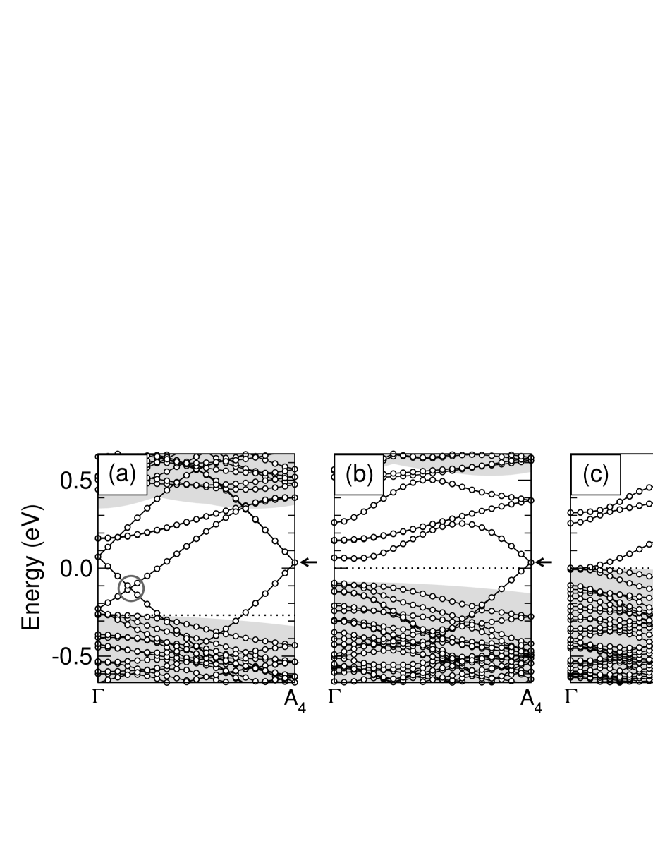
We begin by considering a variant of the full 54 model of Fig. 1 in which the silicon adatoms are absent. When this surface is relaxed within DFT the dimerization vanishes and hence the periodicity reverts to 51. The theoretical band structure for this surface is shown in Fig. 5(a) for wave vectors parallel to the chain direction and energies near the projected band gap. The bands are plotted in the Brillouin zone of the full 54 model so that comparison with the bands of the full model can later be made. The folding of the 51 bands into the 54 zone creates degeneracies at the zone center and the 54 zone boundary A4; the most important zone-boundary degeneracy is marked by an arrow. The folding also creates band crossings, the most important of which (circled) is inside the band gap, about one-fourth of the way from to A4. The Fermi level is very close to the top of the valence band and the system is metallic.
Next we consider how this band structure changes when we dope the surface with extra electrons. It was demonstrated in Fig. 2 that a doping level of 2 electrons per 54 cell leads to stable 52 dimerization, with distortion energetics nearly identical to that from silicon adatoms at 1/4 coverage. Figure 5(b) shows the band structure from this electron-doped surface. The electron doping has two important consequences: the antiferrodistortive dimerization creates a large hybridization gap at the band crossing of the the undoped surface, and the Fermi level is pushed into this gap. The band degeneracy at the 54 zone boundary remains intact (see arrow), because the electron-doped surface has perfect 52 periodicity.
In the presence of silicon adatoms at 1/4 coverage this last degeneracy is lifted. The last two panels of Fig. 5 show the bands calculated at two levels of theory: (c) scalar relativistic; (d) fully relativistic with spin-orbit coupling. (We will show in the next section that the gold character of these surface bands is substantial, hence the spin-orbit splitting is large, about 0.2 eV.) Panel (d) shows that the system now develops a full gap. At 1/4 adatom coverage the Fermi level falls just inside this gap, making the system insulating.
To summarize, we find that silicon adatoms at coverage 1/4 create a multiband metal-insulator transition on Si(111)-(52)-Au. The first (electronically induced) gap arises from band hybridization originating from dimerization and the resultant lowering of symmetry. The second (adatom induced) gap arises from the 54 potential of the adatoms, which lifts the degeneracy at the 54 zone boundary A4.
VI.2 Comparison with angle-resolved photoemission
The above discussion focused on bands above the Fermi level. Now we turn to the occupied states, where we can make direct comparison to experimental data.
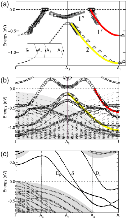
The experimental band structure is highly one-dimensional near the Fermi level, and becomes gradually more two-dimensional for lower energies; here we limit our discussion to the one-dimensional dispersion along the chain direction. The results of our ARPES studies of Si(111)-(52)-Au are summarized in Fig. 6(a), which is reproduced from an earlier publication. mcchesney_phys_rev_b_2004a By combining momentum- and energy-distribution curves from several Brillouin zones, three bands can be identified: , , and . (These labels are used by analogy to comparable bands at stepped Si(111) surfaces.crain_phys_rev_b_2004a ) Figure 6(a) shows the bands in the repeated-zone scheme of a surface with 51 periodicity, for which A1 is the zone boundary. The 52 period doubling introduces backfolded replicas of these bands, shown as dashed lines. The backfolded band is indeed found where expected, indicating that this band has strong 52 character. The backfolded replica of band is too weak to be observed, indicated that it has mainly 51 character. Band becomes more intense as the silicon adatom coverage is increased, indicating that it has strong 54 character.choi_phys_rev_lett_2008a
It is difficult to compare directly the theoretical bands of the adatom-doped surface to these experimental results, because the 52 bands of Fig. 6(a) must be folded once more into the Brillouin zone of the 54 cell. This folding creates many bands in a small energy interval and overly complicates the comparison between theory and experiment. We choose instead a simpler and clearer approximate approach: to compare the experimental 52 bands of Fig. 6(a) to the theoretical 52 bands of the electron-doped surface with no silicon adatoms. In doing so it must be kept in mind that the 54 potential of the adatoms, already seen to play an important role for the unoccupied bands, will be absent.
Figure 6(b) shows the calculated bands for the 52 electron-doped surface, plotted in the 51 repeated-zone scheme used in panel (a). (The projected bulk bands, however, are shown for reasons of clarity in the extended-zone scheme.) The diameter of each circle is proportional to the summed projections of the state onto gold and silicon atoms in the single and double Au-Si chains of Fig. 1. The solid colored curves represent our best effort to match the three strongest surface bands to the ARPES bands. The overall agreement for bands and is excellent, despite the complexity of the calculated bands even for this simplified surface. Note that in our interpretation, and are not simple parabolic bands as depicted in Fig. 6(a). Instead, each comprises two or more bands and exhibits several avoided crossings. Further support for this interpretation will be presented in the next subsection, where we discuss the orbital origin of the bands.
The agreement appears less satisfactory for band . Although this band is correctly centered at the A2 point, and the shallow dispersion near that point reasonable, it is shifted rigidly up in energy by 0.2 eV compared to experiment. We believe that this shift is a spurious effect arising from the omission of silicon adatoms in the calculation. Indeed, Choi et al. have shown experimentally that the band shifts upward as the adatom coverage is reduced. choi_phys_rev_lett_2008a For the range of coverages studied (between 37 and 97% of the saturation 1/4 coverage) the shift in energy was linear. Extrapolating this result to a surface free of adatoms, one naively expects an upward shift in energy of the band by 0.21 eV. Such a shift would bring the results of ARPES and theory into excellent agreement for all three bands.
VI.3 Orbital origin of the bands
We now make one last theoretical simplification by eliminating the extra electrons. Upon relaxation the undoped surface is no longer dimerized, and the periodicity reverts to 51. This simplification is justified if the perturbation of the bands from the dimerization and the extra electrons is small. In the limiting case of zero dimerization the exact 52 bands can be obtained from the 51 bands by simple zone folding. Figure 6(c) shows the calculated band structure for the simplified surface, plotted in the conventional 51 reduced-zone scheme. It is readily apparent that the bands in (b) can indeed be accurately obtained from those in (c) by first folding the 51 bands about the zone midpoint A2, and then shifting the Fermi level upward by the appropriate amount (0.3 eV) for electron doping of rigid bands.
The advantage of the simplified 51 band structure is that its orbital origin is easy to analyze, because the bands fall almost entirely in the projected gap and rarely cross. By examining individual states in real space, we find that the middle band S originates primarily from gold and silicon orbitals in the single chain “Au S” in Fig. 1. The other two bands are more complicated. They arise from the double chain labeled “Au D.” The two bands are the low-lying bonding (Db) and higher-lying antibonding (Da) combinations of orbitals of the gold atoms that constitute each rung of the ladder (combined with orbitals on the connecting silicon atoms).
By comparing the three panels of Fig. 6 we can now understand the orbital origin of the ARPES bands. Band is the simplest and corresponds to the antibonding Da band. Band is a superposition of bands S and Db, which are energetically for energies below the Fermi level. Band has more complicated origin. It arises from two effects: strong rehybridization (related to the dimerization) around A2 of bands S and Db, and the energy shift discussed above from the adatom potential.
We can also now better understand the two gaps created in Fig. 5 by adatom doping. The orbital origin of the those bands can now be assigned by noting, first, that the bands in Fig. 5(a) are identical to those in Fig. 6(c), folded twice along the labeled vertical lines. It should be clear that the electronically induced gap illustrated in Fig. 5(b) arises from hybridization of bands S and Db, which cross near when folded into the 54 zone. Likewise, the adatom-induced gap illustrated in Fig. 5(c) is created entirely within the Da band at the second A4 point, which folds into the A4 zone boundary of the 54 zone.
VII Diffusion of silicon adatoms
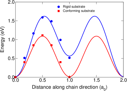
The silicon adatoms decorating Si(111)-(52)-Au are not immobile. hasegawa_phys_rev_b_1996a Sequences of STM images of surfaces prepared with adatom coverage near the equilibrium value 1/8 show evidence for diffusion of adatoms along the Au-Si chain direction, by a defect-mediated mechanism of unknown origin.bussmann_phys_rev_lett_2008a From measurements of the mean-square displacement at different temperatures an effective activation barrier of 1.240.08 eV was extracted.bussmann_phys_rev_lett_2008a In this section we examine whether the structural model proposed in Fig. 1 can account for this diffusion barrier.
Although it is usually straightforward to calculate a barrier for the diffusion of an atom on a well-defined surface, Si(111)-(52)-Au presents an interesting complication. Normally one studies the diffusion of a single atom in a supercell representing the clean surface, and relaxation of the surface around the diffusing atom is allowed. But for Si(111)-(52)-Au the dimerization of the substrate is determined by the location (and coverage) of the adatoms whose very motion is under study. Thus, if the supercell is taken to be 54 and the substrate is allowed to relax, then the phase of the dimerization will track the position of the adatom. This “conforming substrate” is physically unrealistic and will underestimate the true diffusion barrier.
A more plausible scenario, in which the phase of the dimerization remains fixed while the adatom diffuses, is difficult to implement without constraints or a larger supercell. We take a simpler approach and adopt a perfectly rigid 54 substrate, which will overestimate the true barrier. The true barrier must then be between those of the conforming and the rigid substrate.
These two potential energy surfaces were calculated using a 54 unit cell in which the projected position of the adatom along the chain direction was constrained. For the conforming scenario, all other degrees of freedom were relaxed. For the rigid scenario, the two remaining adatom degrees of freedom were relaxed while all other atoms were were fixed at their original 54 positions.
Figure 7 shows the two resulting potential-energy surfaces. For the conforming substrate the potential-energy surface has 52 periodicity and an activation barrier of 1.1 eV, while for the rigid substrate the periodicity is 54 and the activation barrier is 1.6 eV. These two barriers nicely bracket the experimental barrier of 1.24 eV. More detailed studies using realistic boundary conditions will likely play an important role in unraveling the nature of adatom diffusion on this surface.
VIII Outlook
The structural model proposed here for Si(111)-(52)-Au resolves one of the longest-standing unsolved reconstructions of the silicon surface. Predictions based on this model—for the dimerization of the underlying substrate, for the saturation coverage of silicon adatoms, for phase separation into adatom-covered and empty regions, for detailed STM imagery, for electronic band structure, and for the diffusion of adatoms—are in excellent agreement with experiments. Moreover, the physical mechanisms underlying many widely studied phenomena in this system have now been elucidated.
A number of other issues awaiting theoretical study can now be directly addressed. These include, for example, the suggestion that phase separation is accompanied by charge separation and the formation of a Schottky barrier at the interface between adatom-covered and undecorated regions; yoon_phys_rev_lett_2004a the structure and motion of the domain walls, within the Au-Si rows, that form when the spacing between two neighboring adatoms is not commensurate with the 52 substrate; kang_phys_rev_lett_2008a and the exploration of the fundamental limits on using Si(111)-(52)-Au to store and manipulate digital information at densities comparable to that of DNA.bennewitz_nanotechnology_2002a ; kirakosian_surf_sci_2003a
Finally, we anticipate a renewal of theoretical interest in Si(111)-(52)-Au as a physical realization of a nearly one-dimensional metal. Most studies to date have used parametrized models because a definitive structural model has not been available.liu_nanotechnol_2008a With a model in hand, the door is now open to insights from new theoretical investigations as well.
IX Acknowledgements
This work was supported by the Office of Naval Research, and by the NSF under awards No. DMR-0705145 and DMR-0084402 (SRC). S.C.E. gratefully acknowledges many helpful discussions with Christoph Seifert. I. B. acknowledges support from the DAAD. Computations were performed at the DoD Major Shared Resource Center at AFRL.
References
- (1) H. E. Bishop and J. C. Riviere, J. Phys. D Appl. Physics 2, 1635 (1969).
- (2) S. Hasegawa, J. Phys.: Condens. Matter 12, R463 (2000).
- (3) I. Matsuda and S. Hasegawa, J. Phys.: Condens. Matter 19, 355007 (2007).
- (4) I. Barke, R. Bennewitz, J. N. Crain, S. C. Erwin, A. Kirakosian, J. L. McChesney, and F. J. Himpsel, Solid State Comm. 142, 617 (2007).
- (5) I. Barke, T. K. Rügheimer, F. Zheng, and F. J. Himpsel, Appl. Surf. Sci. 254, 4 (2007).
- (6) G. LeLay and J. P. Faurie, Surf. Sci. 69, 295 (1977).
- (7) L. E. Berman, B. W. Batterman, and J. M. Blakely, Phys. Rev. B 38, 5397 (1988).
- (8) T. Hasegawa, K. Takata, S. Hosaka, and S. Hosoki, J. Vac. Sci. Technol. A 8, 241 (1990).
- (9) E. Bauer, Surf. Sci. 250, L379 (1991).
- (10) C. Schamper, W. Moritz, H. Schulz, R. Feidenhans’l, M. Nielsen, F. Grey, and R. L. Johnson, Phys. Rev. B 43, 12130 (1991).
- (11) L. Seehofer, S. Huhs, G. Falkenberg, and R. L. Johnson, Surf. Sci. 329, 157 (1995).
- (12) L. D. Marks and R. Plass, Phys. Rev. Lett. 75, 2172 (1995).
- (13) R. Plass and L. D. Marks, Surf. Sci. 380, 497 (1997).
- (14) J. D. O’Mahony, J. F. McGilp, C. F. J. Flipse, P. Weightman, and F. M. Leibsle, Phys. Rev. B 49, 2527 (1994).
- (15) J. D. O’Mahony, C. H. Patterson, J. F. McGilp, F. M. Leibsle, P. Weightman, and C. F. J. Flipse, Surf. Sci. 277, L57 (1992).
- (16) M. Shibata, I. Sumita, and M. Nakajima, Phys. Rev. B 57, 1626 (1998).
- (17) T. Hasegawa, S. Hosaka, and S. Hosoki, Surf. Sci. 357-358, 858 (1996).
- (18) T. Hasegawa and S. Hosoki, Phys. Rev. B 54, 10300 (1996).
- (19) T. Hasegawa, S. Hosoki, and K. Yagi, Surf. Sci. 355, L295 (1996).
- (20) S. C. Erwin, Phys. Rev. Lett. 91, 206101 (2003).
- (21) M.-H. Kang and J. Y. Lee, Surf. Sci. 531, 1 (2003).
- (22) S. Riikonen and D. Sanchez-Portal, Phys. Rev. B 71, 235423 (2005).
- (23) C. Y. Ren, S. F. Tsay, and F. C. Chuang, Phys. Rev. B 76, 075414 (2007).
- (24) F. C. Chuang, C. H. Hsu, C. Z. Wang, and K. M. Ho, Phys. Rev. B 77, 153409 (2008).
- (25) I. Barke, F. Zheng, S. Bockenhauer, K. Sell, V. v. Oeynhausen, K. H. Meiwes-Broer, S. C. Erwin, and F. J. Himpsel, Phys. Rev. B 79, 155301 (2009).
- (26) Y. Tanishiro, K. Yagi, and K. Takayanagi, Surf. Sci. 234, 37 (1990).
- (27) C. Seifert, Ph.D. thesis, University of Duisburg-Essen, 2006.
- (28) A.-L. Chin and F.-K. Men, Phys. Rev. B 76, 073403 (2007).
- (29) A more realistic value for the gold chemical potential might decrease this energy difference, but is difficult to determine experimentally.
- (30) C. Collazo-Davila, D. Grozea, and L. D. Marks, Phys. Rev. Lett. 80, 1678 (1998).
- (31) L. Lottermoser, E. Landemark, D. M. Smilgies, M. Nielsen, R. Feidenhans’l, G. Falkenberg, R. L. Johnson, M. Gierer, A. P. Seitsonen, H. Kleine, H. Bludau, H. Over, S. K. Kim, and F. Jona, Phys. Rev. Lett. 80, 3980 (1998).
- (32) S. C. Erwin and H. H. Weitering, Phys. Rev. Lett. 81, 2296 (1998).
- (33) S. C. Erwin and C. S. Hellberg, Surf. Sci. 585, L171 (2005).
- (34) G. Lee, S. Hong, H. Kim, D. Shin, J.-Y. Koo, H.-I. Lee, and D. W. Moon, Phys. Rev. Lett. 87, 056104 (2001).
- (35) G. Lee, S. Hong, H. Kim, and J.-Y. Koo, Phys. Rev. B 68, 115314 (2003).
- (36) C. Battaglia, H. Cercellier, C. Monney, M. G. Garnier, and P. Aebi, Europhys. Lett. 77, 36003 (2007).
- (37) C. Battaglia, P. Aebi, and S. C. Erwin, Phys. Rev. B 78, 075409 (2008).
- (38) F.-C. Chuang, C.-H. Hsu, C.-Z. Wang, and K.-M. Ho, Phys. Rev. B 78, 245418 (2008).
- (39) A. Urbieta, K. Schulte, B. Grandidier, D. Deresmes, S. Erwin, and D. Stiévenard, Surf. Sci. 603, 311 (2009).
- (40) R. Doremus, Diffusion of Reactive Molecules in Solids and Melts (Wiley, New York, 2001).
- (41) G. Kresse and J. Hafner, Phys. Rev. B 47, 558 (1993).
- (42) G. Kresse and J. Furthmüller, Phys. Rev. B 54, 11169 (1996).
- (43) J. Tersoff and D. R. Hamann, Phys. Rev. B 31, 805 (1985).
- (44) A. Kirakosian, J. N. Crain, J. L. Lin, J. L. McChesney, D. Y. Petrovykh, F. J. Himpsel, and R. Bennewitz, Surf. Sci. 532, 928 (2003).
- (45) A. Kirakosian, R. Bennewitz, F. J. Himpsel, and L. W. Bruch, Phys. Rev. B 67, 205412 (2003).
- (46) J. L. McChesney, J. N. Crain, V. Perez-Dieste, F. Zheng, M. C. Gallagher, M. Bissen, C. Gundelach, and F. J. Himpsel, Phys. Rev. B 70, 195430 (2004).
- (47) H. S. Yoon, J. E. Lee, S. J. Park, I. W. Lyo, and M. H. Kang, Phys. Rev. B 72, 155443 (2005).
- (48) W. H. Choi, P. G. Kang, K. D. Ryang, and H. W. Yeom, Phys. Rev. Lett. 100, 126801 (2008).
- (49) E. Bussmann, S. Bockenhauer, F. J. Himpsel, and B. S. Swartzentruber, Phys. Rev. Lett. 101, 266101 (2008).
- (50) P. G. Kang, H. Jeong, and H. W. Yeom, Phys. Rev. Lett. 100, 146103 (2008).
- (51) R. Bennewitz, J. N. Crain, A. Kirakosian, J.-L. Lin, J. L. McChesney, D. Y. Petrovykh, and F. J. Himpsel, Nanotechnology 13, 499 (2002).
- (52) A. A. Baski, J. Nogami, and C. F. Quate, Phys. Rev. B 41, 10247 (1990).
- (53) I. R. Collins, J. T. Moran, P. T. Andrews, R. Cosso, J. D. O’Mahony, J. F. McGilp, and G. Margaritondo, Surf. Sci. 325, 45 (1995).
- (54) T. Okuda, H. Daimon, H. Shigeoka, S. Suga, T. Kinoshita, and A. Kakizaki, J. Electron Spectroscopy and Rel. Phenom. 80, 229 (1996).
- (55) T. Okuda, H. Daimon, S. Suga, Y. Tezuka, and S. Ino, Appl. Surf. Sci. 121, 89 (1997).
- (56) I. G. Hill and A. B. McLean, Phys. Rev. B 55, 15664 (1997).
- (57) I. G. Hill and A. B. McLean, Appl. Surf. Sci. 123-124, 371 (1998).
- (58) R. Losio, K. N. Altmann, and F. J. Himpsel, Phys. Rev. Lett. 85, 808 (2000).
- (59) K. N. Altmann, J. N. Crain, A. Kirakosian, J.-L. Lin, D. Y. Petrovykh, F. J. Himpsel, and R. Losio, Phys. Rev. B 64, 035406 (2001).
- (60) F. J. Himpsel, K. N. Altmann, J. N. Crain, A. Kirakosian, J. L. Lin, A. Liebsch, and V. P. Zhukov, J. Electron Spectroscopy and Related Phenomena 126, 89 (2002).
- (61) H. M. Zhang, T. Balasubramanian, and R. I. G. Uhrberg, Phys. Rev. B 65, 035314 (2001).
- (62) J. N. Crain, J. L. McChesney, F. Zheng, M. C. Gallagher, P. C. Snijders, M. Bissen, C. Gundelach, S. C. Erwin, and F. J. Himpsel, Phys. Rev. B 69, 125401 (2004).
- (63) H. S. Yoon, S. J. Park, J. E. Lee, C. N. Whang, and I. W. Lyo, Phys. Rev. Lett. 92, 096801 (2004).
- (64) C. H. Liu, T. Inaoka, S. Yaginuma, T. Nakayama, M. Aono, and T. Nagao, Nanotechnol. 19, 355204 (2008).