Electric charge enhancements in carbon nanotubes :
Theory and experiments
Abstract
We present a detailed study of the static enhancement effects of electric charges in m-long single-walled carbon nanotubes, using theoretically an atomic charge-dipole model and experimentally electrostatic force microscopy. We demonstrate that nanotubes exhibit at their ends surprisingly weak charge enhancements which decrease with the nanotube length and increase with the nanotube radius. A quantitative agreement is obtained between theory and experiments.
pacs:
73.63.Fg, 68.37.Ps, 85.35.Kt, 41.20.CvUnderstanding of the properties of electric charges in carbon nanotubes (CNTs) is one of the important issues for their promising applications in nanoelectromechanical systems,Anantram and Leonard (2006) field emission,De Heer et al. (1995) chemical sensorsSnow et al. (2005) and charge storage.An et al. (2001); Cui et al. (2002); Ryu et al. (2007) A key-aspect of the electrostatics of these one-dimensional systems is the knowledge of the distribution of electric charges along the nanotubes, because charges are likely to accumulate at the nanotube ends due to Coulomb repulsion. Theoretical predictions have been established for this effect, but not in the range of lengths accessible from experiments, so that no comparison has been established between theory and experimental observations so far. More precisely, the electrostatic properties of single-walled nanotubes (SWCNTs) have been addressed on the one hand using electric force microscopy (EFM) experimentsBockrath et al. (2002); Jespersen and Nygard (2007) coupled to charge injection techniquesPaillet et al. (2005); Zdrojek et al. (2006a). Results obtained for m-long nanotubes indicated that electric charges are distributed rather uniformly along the tube length, with however no theoretical support in this range of nanotube length. On the other hand, in theoretical studies, density functional theoryKeblinski et al. (2002) and classical electrostaticsLi and Chou (2006) calculations have been performed to compute the charge distribution in SWCNTs, and have predicted -like shapes due to a charge accumulation at the nanotube ends. These calculations however only hold for short ( nm) nanotube lengths, which are not easily accessible from experiments.
It is the scope of this paper to provide a combined experimental and theory work on this issue. We present a detailed study of the static enhancement effects of electric charges in SWCNTs, using theoretically an atomic charge-dipole model and experimentally electrostatic force microscopy. It is demonstrated that the U-like shape of the charge distribution expected for short nanotubes is replaced in the case of m-long tubes by weak charge enhancements localized at the nanotube ends, in agreement with the experimental values for the enhancement factors (up to few tens of %) observed from EFM and charge injection experiments. The dependence of the charge enhancement factors on the nanotube radius has also been measured from EFM experiments, and falls in quantitative agreement with theoretical preditions for m-long tubes.
The paper is organized as follows : we first describe the numerical calculations of the charge distribution along nanotubes using the atomic charge-dipole model and the results obtained for short nanotubes with open or closed caps, either considered in vacuum or on a SiO2 substrate. The extrapolation procedure to the case of m-long nanotubes is then presented, and compared with experimental EFM measurements of charge enhancement factors on SWCNTs. We finally discuss the dependence of the enhancement factors as a function of the nanotube radius.
In the theoretical calculations presented throughout this work, the interactions between the electric charges and the induced dipoles are described using the Gaussian-regularized atomic charge-dipole interaction model,Mayer (2007); Mayer and Astrand (2008) in which the atoms are treated as interacting polarizable points with free charges, and the distribution of charges and dipoles are determined by the fact that their static equilibrium state should correspond to the minimum value of the total molecular electrostatic energy. Compared with classical Coulomb-law-based models in which only charges are considered, this model provides a more accurate description of electrostatic properties of CNTs, since the charges, the induced dipoles and the atomic polarizabilities are taken into account.
In order to achieve a valid comparison between experimental data and calculation results, the effect of a SiO2 substrate (nanotubes are usually deposited on a SiO2 thin film in experiments) is also taken into account in our calculations, by adding surface-induced terms to the vacuum electrostatic interaction tensors using the method of mirror images.Jackson (1975) The dielectric constant of SiO2 is taken as . The average distance between the bottom of the tubes and the SiO2 surface is set to nm after the computed CNT-SiO2 long-range interacting configurations from Refs.Tsetseris and Pantelides (2006); Wojdel and Bromley (2005). Furthermore, we note that can slightly vary with the tube radius . It will however be fixed to nm in this work as an average value. The atomic structure of CNTs is then optimized by energy minimization using the method of conjugated gradient based on a many-body chemical potential model AIREBO (adaptive interatomic reactive empirical bond order).Stuart et al. (2000) Linear charge densities of 0.055/nm have been used in calculations, so as to match linear charge densities observed experimentally.Zdrojek et al. (2008)
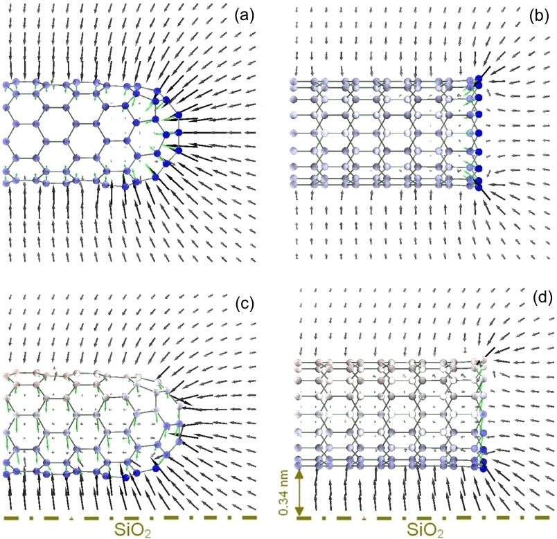
To illustrate the typical outputs of the atomic-scale calculations, we show in Fig. 1 the charge distribution at the end of a (9, 0) CNT of length nm and average charge density atom. The color of the atoms is proportional to their charge in the figure. We represented here for sake of clarity the four distinct situations in which the nanotube exhibits either a closed (Fig. 1a and c) or an open (Fig. 1b and d) cap structure, and the tube is either considered in vacuum (Fig. 1a and b) or deposited on a SiO2 substrate (Fig. 1c and d). As seen from Fig. 1, the charge density at the tube ends is higher than that at other parts of the tubes in all situations. The maximum charge density on the opened cap is here about twice that on the closed one for this small-radius tube. Finally, when the tube is deposited on the SiO2 surface, electrons are attracted by their image charge towards the SiO2 surface, as a typical semi-space effect.
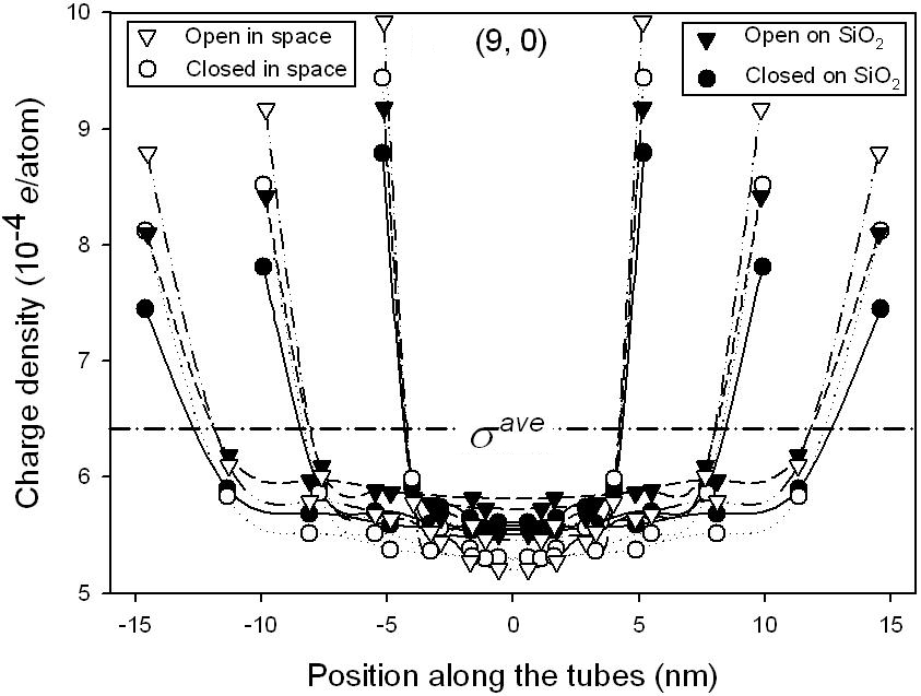
Since the nanotubes used in experiments have lengths in the micrometer range, and since this scale can hardly be directly addressed by calculations using atomic models due to the limit of computational resources, the issue about the relationship between the tube length and the charge distribution needs to be carefully addressed, so as to later extrapolate charge enhancement factors to the length scales of interest in experiments. The length dependence of the charge enhancements at the nanotube ends is illustrated in Fig. 2, in which we plotted the local average charge density as a function of the position along the nanotube (the -axis origin in Fig. 2 corresponds to the nanotube midpoint). The local average charge density is defined from the charge carried by individual CNT atoms, when averaged along the nanotube circumference and along a fraction of the length of the CNT (this fraction is taken as 10% in Fig. 2). is the quantity which can be accessed experimentally from EFM techniques.Zdrojek et al. (2008) The typical shape of the CNT charge distribution observed in Fig. 2 corresponds to the U-like shape expected for short nanotubes, Keblinski et al. (2002) but the charge enhancement at the tube ends is already seen to become less significant when the tube gets longer. Furthermore, we can also see that the charge enhancement is weaker when the ends of the tubes are closed and when the nanotubes are placed on the SiO2 surface. The latter effect can be understood by the fact that the net nanotube charge is located at the CNT side close to the substrate (see Fig. 1 (c) and (d)), which leads to an effective reduction of the charge-distributed area in the non-axial direction, similar to an effective decrease of the nanotube radius , which will be discussed further in this paper (see Fig. 6).
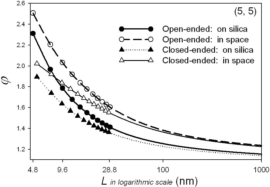
We now focus on charge enhancements for m-long nanotubes, and their comparison with experimental results. Since the spatial resolution in EFM experiments is about nm (this resolution is mostly limited by the tip-substrate separation during EFM detection), we now consider the enhancement zone in our calculation as a zone of length at the tube end, and define the charge enhancement ratio as the ratio between the charge density averaged in the zone of length at the end of the nanotube, and the charge density at the center of the nanotube. The influence of the tube length on the charge enhancement ratio is shown in Fig. 3. is seen to decrease significantly with for short tubes (particularly for nm), but the variations get smaller when the tube is longer. Note that is independent of , because the local charge densities should be proportional to the total one by requiring a constant electric potential on the tube surface. Furthermore, we find that if the (open or closed) cap structure plays an important role in the charge enhancement for short tubes ( nm) (as seen in Fig. 1 ), this effect already becomes unsignificant for nm, and will become negligible for m-long nanotubes in experiments with resolution. Finally, it appears that the only parameter that needs to be properly taken into account is the presence of the SiO2 surface below the nanotube, which still effectively reduces the charge enhancement ration for nm.
In order to extrapolate these results towards m-long nanotubes, we performed a fit of the data points of Fig. 3. Since the the analytical formula of the exact distribution of charge on a hollow tube is not known in the literature, we used the equation : , in which are four fitted parameters for each nanotube radius. This phenomenological equation has been chosen since it describes a ratio between two cylindrical capacitances, and is thus well-suited to account for , which is the ratio between the linear charge densities at the end and at the middle of the nanotube. The lines in Fig. 3 correspond to the fits obtained independently for the nanotubes with either open or closed caps, vacuum environment, or SiO2 surface. The extrapolated values for are seen to converge for large for open and closed cap structures, but to differ depending on the vacuum or SiO2 environment. This behaviour is in full agreement with the trend observed on the atomic calculation points obtained for nm, which already brings confidence at this stage about the validity of our extrapolation procedure.
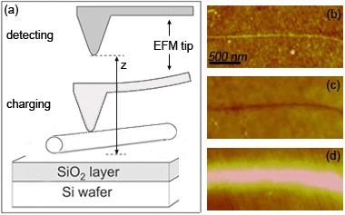
Our theoretical predictions are finally compared with electrostatic measurements performed by injecting and detecting charges in individual CNTs using electrostatic force microscopy. In these experiments, nanotubes grown by chemical vapour deposition are deposited from dichloromethane solutions onto silicon wafers covered by a 200nm-thick thermal dioxide layers. Individual nanotubes are located by atomic force microscopy, and then charged (see Fig. 4 (a)) by pressing the biased tip of an atomic force microscope on the nanotube (typically with an injection bias V, pressing force of a few nN). The CNT charge state is then measured before and after injection by EFM, by recording electrostatic force gradients acting on the tip which is intentionally lifted at a distance about - nm above the sample surface to discard short range surface forces. Fig. 4 (b) shows the topography image of a SWCNT. In Fig. 4 (c), the EFM scan of the tube before charging is shown, as a dark footprint of the CNT topography associated with attractive forces due to the nanotube capacitance. It can be shown experimentally that the negative frequency shifts are here of capacitive origin, and not originating in a positive charge transferred from the substrate to the nanotube (see details in Ref. Zdrojek et al. (2006a)). The nanotube EFM image after charge injection is shown in Fig. 4 (d). The tube is seen here as a bright feature as a result of the negative charges injected in the tube. From previous EFM studies, we have shown that the charge imaged for SWCNTs mainly correspond to charge emitted from the tube and “printed” in the oxide layer in the vicinity of the nanotube.Zdrojek et al. (2006b); Paillet et al. (2005)
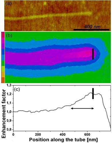
To compare these predictions with our calculation results, we show in Fig. 5 the charge distribution at the end of a SWCNT (total length 2 m) after a charge injection experiment. A non-linear color scale has been used in Fig. 5b in order to evidence the weak charge enhancement localized within nm at the nanotube end. The charge distribution along the nanotube is shown in Fig. 5c, in which we plotted the charge enhancement factor measured from EFM, defined as the ratio of the EFM signal with that measured at the middle of the nanotube. From these experimental data, one gets the maximum value for this tube (see Fig. 5 (c)), in agreement with the numerical extrapolation from theoretical results predicting for a m tube with nm deposited on a SiO2 surface.
To further validate the comparison of our theoretical predictions with experiments, we now focus on the dependence of the charge enhancement ratio as a function of the nanotube radius . Such an analysis would not be possible for short nanotubes, because the charge enhancement ratio would then be strongly dependent on the nanotube cap structure, as discussed previously (see Fig. 3), while this effect is not relevant for m-long naontubes. Intuitively, one can guess that the nanotube charge enhancement factor will increase with the tube radius , because the enhancement factor decreases with the nanotube length : increasing at fixed length reduces the nanotube anisotropy, and is qualitatively similar as decreasing the nanotube length for a fixed radius .
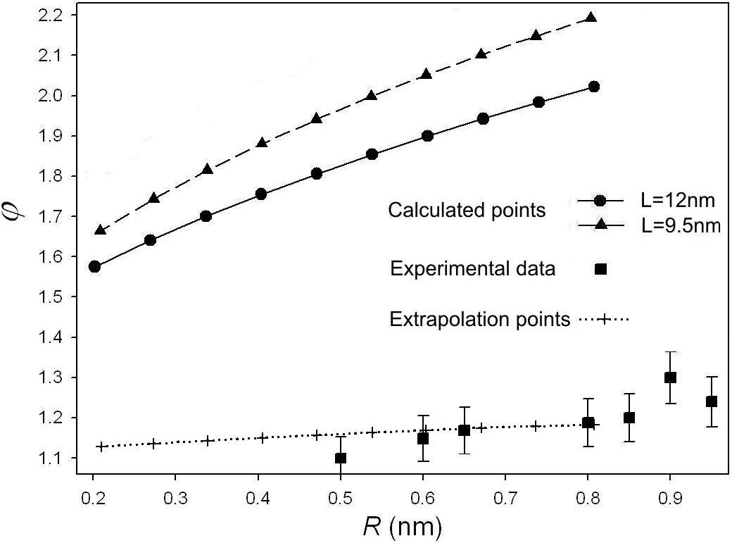
Experimentally, we measured the charge densities along seven SWCNTs with lengths between 1 and 9 m in a similar way as in Fig. 5 (c), and plotted the corresponding charge enhancement ratios in Fig. 6, as a function of the nanotube radius measured from atomic force topography images. The error bars on correspond here to the accuracy of the EFM measurements. Experimental data points clearly show that slightly increases as a function of the nanotube radius . The possibility to observe this behavior also confirms that the values of on m-long nanotubes do not critically depend on the tube length, nor on the nanotube cap structure. Numerical calculations for the charge enhancement ratio have also been performed using nanotubes with different radius , and are shown in Fig. 6. Direct calculations of obtained from the atomic dipole-charge models and using an averaging over 10% are given in Fig. 6 for two short nanotubes (9 and 12 nm, solid circles and triangles), as well as calculation results obtained for m-long nanotubes (dotted line) using the extrapolation procedure described in Fig. 3. Theoretical predictions are seen to quantitatively agree with experimental data within experimental error bars, and confirm the increase of the charge enhancement ratio as a function of the nanotube radius. The values of computed with 5% and 15% for m length tubes (data not shown) also vary within experimental error bars.
In summary, we have characterized the enhancement of net electric charge in SWCNTs by both atomic-model calculations and EFM experiments. We have demonstrated that the U-like shape of the charge distribution expected for short nanotubes is replaced for m-long nanotubes by weak charge enhancements localized at the nanotube ends, while the nanotube charge densities are otherwise almost constant along the nanotubes. The dependence on the tube length, nanotube cap structure, and the influence of silica substrate have been investigated. It has been shown that the charge enhancement at the ends of CNTs depends strongly on the geometry of the cap only for short tubes ( nm), but has an insignificant influence for nanotubes with lengths in the micrometer range. The increase of the charge enhancement ratio with the nanotube radius has been demonstrated experimentally, in quantitative agreement with theoretical predictions.
We expect that the mapping and the understanding of the charge enhancement of CNTs are important for many applications, besides the fundamental character of this study, e.g. imaging of field and charge in CNTs electronic circuitsBachtold et al. (2000); De Pablo et al. (2001) or emission devices modified by the presence of surfaces. The electrostatic response of nanotubes appears to be strongly sensitive to its environment, which is of high importance for nanotube based sensors.Snow et al. (2005); Robinson et al. (2006) This work can also have implication in the field of nano-electromechanical systems and charge storage devices.
This work is a part of the CNRS GDR-E No. 2756. Z. W. acknowledges the support from the region of Franche-Comté (grant 060914-10).
References
- Anantram and Leonard (2006) M. Anantram and F. Leonard, Rep. Prog. Phys. 69, 507 (2006).
- De Heer et al. (1995) W. De Heer, A. Chatelain, and D. Ugarte, Science 270, 1179 (1995).
- Snow et al. (2005) E. Snow, F. Perkins, E. Houser, S. Badescu, and T. Reinecke, Science 307, 1942 (2005).
- An et al. (2001) K. An, W. Kim, Y. Park, Y. Choi, S. Lee, D. Chung, D. Bae, S. Lim, and Y. Lee, Adv. Mater. 13, 497 (2001).
- Cui et al. (2002) J. Cui, R. Sordan, M. Burghard, and K. Kern, Appl. Phys. Lett. 81, 3260 (2002).
- Ryu et al. (2007) S.-W. Ryu, X.-J. Huang, and Y.-K. Choi, Appl. Phys. Lett. 91, 063110 (2007).
- Bockrath et al. (2002) M. Bockrath, N. Markovic, A. Shepard, M. Tinkham, L. Gurevich, L. Kouwenhoven, M. Wu, and L. Sohn, Nano Letters 2, 187 (2002).
- Jespersen and Nygard (2007) T. Jespersen and J. Nygard, Appl. Phys. A 88, 309 (2007).
- Paillet et al. (2005) M. Paillet, P. Poncharal, and A. Zahab, Phys. Rev. Lett. 94, 186801 (2005).
- Zdrojek et al. (2006a) M. Zdrojek, T. Mélin, H. Diesinger, D. Stiévenard, W. Gebicki, and L. Adamowicz, J. Appl. Phys. 100, 114326 (2006a).
- Keblinski et al. (2002) P. Keblinski, S. Nayak, P. Zapol, and P. Ajayan, Phys. Rev. Lett. 89, 255503 (2002).
- Li and Chou (2006) C. Li and T.-W. Chou, Appl. Phys. Lett. 89, 063103 (2006).
- Mayer (2007) A. Mayer, Phys. Rev. B 75, 045407 (2007).
- Mayer and Astrand (2008) A. Mayer and P.-O. Astrand, J. Phys. Chem. A 112, 1277 (2008).
- Jackson (1975) J. D. Jackson, Classical Electrodynamics (Wiley, New York, 1975), p. 54-62.
- Tsetseris and Pantelides (2006) L. Tsetseris and S. Pantelides, Phys. Rev. Lett. 97, 266805 (2006).
- Wojdel and Bromley (2005) J. Wojdel and S. Bromley, J. Phys. Chem. B 109, 1387 (2005).
- Stuart et al. (2000) S. J. Stuart, A. B. Tutein, and J. A. Harrison, J. Chem. Phys. 112, 6472 (2000).
- Zdrojek et al. (2008) M. Zdrojek, T. Heim, D. Brunel, A. Mayer, and T. Mélin, Phys. Rev. B 77, 033404 (2008).
- Zdrojek et al. (2006b) M. Zdrojek, T. Mélin, H. Diesinger, D. Stiévenard, W. Gebicki, L. Adamowicz, Phys. Rev. Lett. 96, 039703 (2006b).
- Paillet et al. (2005) M. Paillet, P. Poncharal, and A. Zahab, Phys. Rev. Lett. 96, 039704 (2006).
- Bachtold et al. (2000) A. Bachtold, M. Fuhrer, S. Plyasunov, M. Forero, E. Andersen, A. Zettl, and P. McEuen, Phys. Rev. Lett. 84, 6082 (2000).
- De Pablo et al. (2001) P. De Pablo, C. Gomez-Navarro, A. Gil, J. Colchero, M. Martinez, A. Benito, W. Maser, J. Gomez-Herrero, and A. Baro, Appl. Phys. Lett. 79, 2979 (2001).
- Robinson et al. (2006) J. Robinson, E. Snow, S. Badescu, T. Reinecke, and F. Perkins, Nano Letters 6, 1747 (2006).