SQUIPT - Superconducting Quantum Interference Proximity Transistor
Abstract
We present the realization and characterization of a novel-concept interferometer, the superconducting quantum interference proximity transistor (SQUIPT). Its operation relies on the modulation with the magnetic field of the density of states of a proximized metallic wire embedded in a superconducting ring. Flux sensitivities down to Hz-1/2 can be achieved even for a non-optimized design, with an intrinsic dissipation ( fW) which is several orders of magnitude smaller than in conventional superconducting interferometers. Our results are in agreement with the theoretical prediction of the SQUIPT behavior, and suggest that optimization of the device parameters would lead to a large enhancement of sensitivity for the detection of tiny magnetic fields. The features of this setup and their potential relevance for applications are further discussed.
Proximity effect degennes is a phenomenon which can be described as the induction of superconducting correlations into a normal-type conductor heersche ; jherrero ; keizer ; morpurgo ; kasumov ; cleuziou ; doh ; xiang ; pothier ; courtois ; morpurgo1 ; giazotto ; baselmans . One striking consequence of this effect is the modification of the local density of states (DOS) in the normal metal belzig ; belzig2 ; gueron ; sueur , and the opening of a minigap belzig2 ; belzig ; zhou whose amplitude can be controlled by changing the macroscopic phase of the superconducting order parameter belzig ; sueur . Here we report the realization of a novel interferometer, the superconducting quantum interference proximity transistor (SQUIPT), whose operation relies on the modulation with the magnetic field of the DOS of a proximized metal embedded in a superconducting loop. Flux sensitivities down to Hz-1/2 ( Wb is the flux quantum) can be achieved even for a non-optimized design, with an intrinsic dissipation which is several orders of magnitude smaller than in conventional superconducting interferometers clarke ; tinkham ; likharev . Optimizing the device parameters promises to largely increase the sensitivity for the detection of tiny magnetic fields.
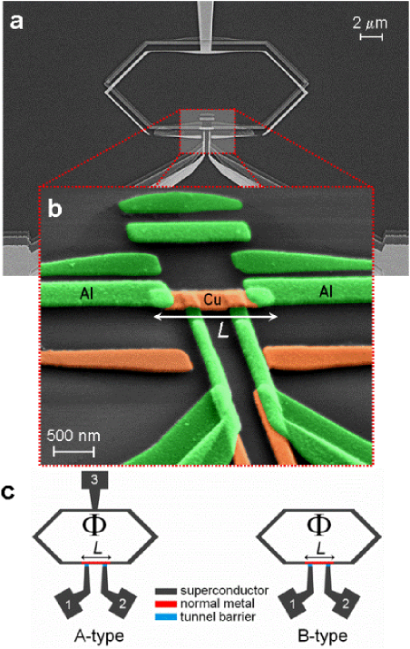
One typical SQUIPT fabricated with electron-beam lithography is shown in Fig. 1(a). It consists of an aluminum (Al) superconducting loop interrupted by a copper (Cu) normal metal wire in good electric contact with it. Furthermore, two Al electrodes are tunnel-coupled to the normal region to allow the device operation. A blow-up of the sample core [see Fig. 1(b)] displays the Cu region of length m and width nm coupled to the tunnel probes and the superconducting loop. The SQUIPTs were implemented into two different designs [see Fig. 1(c)], namely, the A-type configuration, where the loop extends into an additional third lead, and the B-type configuration which only contains two tunnel probes. The ring geometry allows to change the phase difference across the normal metal-superconductor boundaries through the application of an external magnetic field which gives rise to a total flux through the loop area. This modifies the DOS in the normal metal, and hence the transport through the tunnel junctions.
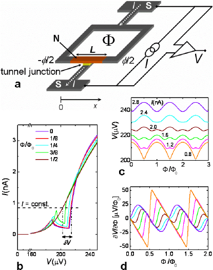
Insight into the interferometric nature of the SQUIPT can be gained by analyzing first of all the theoretical prediction of its behavior. Figure 2(a) sketches the simplest implementation of the device in the A-type configuration, i.e., that with just one junction tunnel-coupled to normal metal. For simplicity we suppose the tunnel probe (with resistance ) to be placed in the middle of the wire, and to feed a constant electric current through the circuit while the voltage drop is recorded as a function of . In the limit that the kinetic inductance of the superconducting loop is negligible, the magnetic flux fixes a phase difference across the normal metal, where is the flux quantum, the Planck’s constant, and the electron charge. Figure 2(b) shows the low-temperature quasiparticle current-voltage () characteristic of the SQUIPT calculated at a few selected values of . The calculations were performed for parameters similar to those of our structures sns . It clearly appears that while for , i.e., when the minigap in the normal metal is maximized sueur ; zhou , the characteristic resembles that of a superconductor-insulator-superconductor junction tinkham , for the characteristic corresponds to that of a normal metal-insulator-superconductor contact, with the minigap suppressed sueur ; zhou . The SQUIPT thus behaves as a flux-to-voltage transformer whose response (and amplitude ) depends on the bias current through the tunnel junction. The interferometer voltage modulation is shown in Fig. 2(c) for different values of . In particular, is strongly dependent on the bias current, the latter determining the exact shape of the device response. Note the change of concavity of which occurs as the bias current exceeds the point where the characteristics cross. One relevant figure of merit of the SQUIPT is represented by the flux-to-voltage transfer function, , which is shown in Fig. 2(d). It turns out that is a non-monotonic function of the bias current, as well as its sign depends on the specific value of .
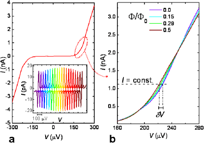
Figure 3(a) displays the experimental low-temperature characteristic of a device implemented in the A-type configuration. The curve resembles that of a typical superconducting tunnel junction, where the onset of large quasiparticle current is set by the energy gap (eV in our samples). The absence of the peak in the experimental curves, as compared to the theoretical ones in Fig. 2(b), could originate from broadening due to inelastic scattering or finite quasiparticle lifetime in the superconductor timofeev . A deeper inspection reveals, however, that the characteristic is modulated by the presence of an applied magnetic field. The effect is clearly visible in Fig. 3(b) which shows the blow-up of the curve at large bias voltage for some values of the applied flux up to . Such a modulation is of coherent nature, and stems from magnetic field-induced control of the DOS in the normal metal. In addition to the quasiparticle current, a Josephson coupling is observed at the lowest temperatures, and manifests itself as a peak around zero bias in the characteristic [see the inset of Fig. 3(a)]. The supercurrent, which is expected to exist in proximized structures like the present one belzig , obtains values as high as pA at 53 mK. It is modulated by the applied flux with the same periodicity as for the quasiparticle current.
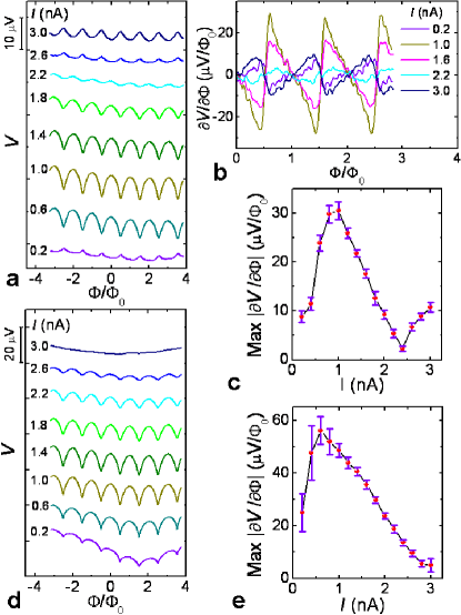
The full dependence for the same A-type sample at several values of the bias current is shown in Fig. 4(a). As expected [see Fig. 2(c)], the modulation amplitude is a non-monotonic function of , while shows changing of concavity whenever the bias current exceeds the crossing points of the current-voltage characteristic [see Fig. 3(b)]. In this sample obtains values as large as V at 1 nA. The corresponding transfer function is displayed in Fig. 4(b) for a few bias currents. Resemblance with theoretical prediction of Fig. 2(c) and 2d is obvious. In such a case as large as is obtained at 1 nA. The maximum of for the same SQUIPT is displayed in Fig. 4(c), and highlights the expected non-monotonic dependence on .
Figure 4(d) and 4e show and the maximum of , respectively, for a B-type SQUIPT . obtains in this case values as high as V at 1 nA, while is maximized at 0.6 nA where it reaches . We emphasize that these values are larger by almost a factor of two than those obtained in the A-type device. This is to be expected since in a B-type sample is probed across two tunnel junctions in series. This doubles the SQUIPT response. The above results are roughly of those predicted by our calculations [see Fig. (2)], which can be ascribed either to the uncertainty in the precise determination of the device parameters sns or to non-ideal phase biasing of the interferometers sueur . In the limit of negligible geometric inductance of the loop ( pH for our rings), a phase difference can be induced across the normal metal if the phase accumulated in the superconductor is much smaller than that accumulated in the wire, i.e., if the ratio between their respective kinetic inductances is much smaller than unity. The correction factor to the actual phase bias determined by such a ratio (estimated to be around for our devices) may prevent the full closing of the minigap, thus weakening the SQUIPT response.
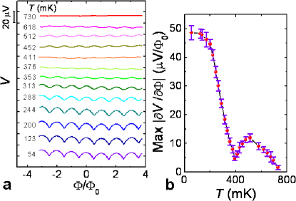
The role of temperature () is shown in Fig. 5(a) which displays at 1 nA for several increasing temperatures for a B-type sample. initially monotonically decreases with increasing up to mK, then it starts to increase again and it is almost suppressed at mK. The full temperature dependence of the maximum of at 1 nA is shown in Fig. 5(b) for the same device, and reflects the above non-monotonic behavior similarly to that observed for different bias currents [see Fig. 4(c)].
Compared to conventional DC superconducting quantum interference devices (SQUIDs) clarke ; tinkham ; likharev , power dissipation () is dramatically suppressed in the SQUIPT. In our devices we have fW, which can be further reduced by simply increasing the resistance of the probing junctions. This power is 4 - 5 orders of magnitude smaller than that in conventional DC SQUIDs, which makes the SQUIPT ideal for applications where very low dissipation is required.
We shall finally comment on another figure of merit of the SQUIPT, namely, its noise-equivalent flux (NEF) or “flux sensitivity” defined as likharev , where is the voltage noise of the interferometer within the frequency band . In our experiment we can provide an upper estimate for NEF, since it is believed to be limited mainly by the preamplifier noise. With a typical rms noise of nV/ in our setup, we estimate at best, which should be substantially higher than the SQUIPT intrinsic NEF. We note that the preamplifier contribution to the noise can be made negligible by increasing , i.e., by optimizing the SQUIPT parameters and the phase bias as well. Our calculations show that by replacing niobium (Nb) as the superconductor (with meV), and by shortening down to nm, as large as mV could be achieved yielding . The device intrinsic noise deserves however further investigation.
The SQUIPT has a number of features which make it attractive for a variety of applications: (1) only a simple DC read-out scheme is required, similarly to DC SQUIDs; (2) either current- or voltage-biased measurement can be conceived depending on the setup requirements; (3) a large flexibility in the fabrication parameters and materials, such as semiconductors doh ; xiang ; morpurgo1 ; giazotto , carbon nanotubes jherrero ; morpurgo ; cleuziou or graphene heersche instead of normal metals, is allowed to optimize the response and the operating temperature (to this end superconducting V garcia or Nb are suitable candidates); (4) ultralow dissipation ( fW) which makes it ideal for nanoscale applications; (5) ease of implementation in a series or parallel array (depending on the biasing mode) for enhanced output; (6) ease of integration with superconducting refrigerators rmp to actively tune the device working temperature. Our approach opens the way to magnetic-field detection based on “hybrid” interferometers which take advantage of the flexibility intrinsic to proximity metals.
We gratefully acknowledge O. Astafiev, L. Faoro, R. Fazio, M. E. Gershenson, T. T. Heikkil, L. B. Ioffe, V. Piazza, P. Pingue, F. Portier, H. Pothier, H. Rabani, F. Taddei, and A. S. Vasenko for fruitful discussions. The work was partially supported by the INFM-CNR Seed project “Quantum-Dot Refrigeration: Accessing the K Regime in Solid-State Nanosystems”, and by the NanoSciERA project “NanoFridge”.
I Supplementary information, methods used in sample fabrication, measurements and theoretical analysis
Fabrication details and experimental setup. The samples were fabricated at the Low Temperature Laboratory at Helsinki University of Technology by standard three-angle shadow-mask evaporation of the metals through a conventional suspended resist mask in a single vacuum cycle. Initially, a bi-layer PMMA/copolymer resist was spun on an oxidized Si wafer, onto which the structures were patterned using electron-beam lithography. In the electron-gun evaporator, the chip was first tilted to an angle of with respect to the source, and approximately 27 nm of Al was evaporated to create the superconducting electrodes of the probe tunnel junctions. To form the tunnel barriers, the sample was exposed to 4.4 mbar of oxygen for five minutes, and consequently tilted to for the deposition of 27 nm of Cu forming the normal metal island. Immediately after this, the chip was tilted to the final angle of , and 60 nm of Al was deposited to form the superconducting loop and the transparent normal metal-superconductor contacts. The magneto-electric characterization was performed at NEST CNR-INFM by cooling the devices with a filtered 3He/4He dilution refrigerator down to mK. Current and voltage were measured with room-temperature preamplifiers.
Theoretical model. The considered system consists of a one-dimensional diffusive normal-metal wire of length in good electric contact with two superconducting leads which define a ring [see Fig. 2(a)]. The contact with the superconductors allows superconducting correlations to be induced into the normal-metal region through proximity effect degennes , that is responsible for the modification of the density of states (DOS) in the wire belzig2 , as well as for the Josephson current to flow through the superconductor-normal metal-superconductor structure belzig . The proximity effect in the normal-metal region of the SQUIPT can be described with the Usadel equations usadel which can be written as usadel ; belzig
| (1) |
where is the diffusion constant and is the energy relative to the chemical potential in the superconductors. and are, in general, complex scalar functions of position and energy. For perfectly-transmitting interfaces the boundary conditions at the normal metal-superconductor contacts [i.e., , see Fig. 2(a)] reduce to and , where is the phase difference across the normal metal-superconductor boundaries, and is the superconducting order parameter. For simplicity we chose a step-function form for the order parameter, i.e., constant in the superconductor and zero in the normal-metal region, although is in principle position-dependent and can be determined self-consistently belzig . The DOS in the normal-metal region normalized to the DOS at the Fermi level in the absence of proximity effect is given by . From the numerical solution of Eqs. (1) we get the DOS as a function of position and energy for any given . In particular, the DOS is an even function of energy, and exhibits a minigap () for belzig2 whose magnitude depends in general on the Thouless energy , the characteristic energy scale for the normal region, and on . The minigap is maximum for and decreases with increasing , vanishing at zhou (the behavior is -periodic in ).
The quasiparticle current () through the superconducting tunnel junction biased at voltage [see Fig. 2(a)] can be calculated from wolf
| (2) |
where is the electron charge, is the tunnel junction resistance, is the Bardeen-Cooper-Schrieffer normalized DOS in the superconductor, is the Heaviside step function, is the Fermi-Dirac distribution function at temperature , and is the Boltzmann constant. For any bias current () imposed across the SQUIPT, the voltage response is determined from the solution of the equation . From this, we calculate the flux-to-voltage transfer function .
References
- (1) P. G. de Gennes, Superconductivity of Metals and Alloys (W. A. Benjamin, New York, 1966).
- (2) H. B. Heersche, P. Jarillo-Herrero, J. B. Oostinga, L. M. K. Vandersypen, and A. F. Morpurgo, Nature 446, 56 (2007).
- (3) P. Jarillo-Herrero, J. A. van Dam, and L. P. Kouwenhoven, Nature 439, 953 (2006).
- (4) R. S. Keizer et al., Nature 439, 825 (2006).
- (5) A. F. Morpurgo, J. Kong, C. M. Marcus, and H. Dai, Science 286, 263 (1999).
- (6) A. Yu. Kasumov et al., Science 291, 280 (2001).
- (7) J.-P. Cleuziou, W. Wernsdorfer, V. Bouchiat, T. Ondarcuhu, and M. Monthioux, Nature Nanotech. 1, 53 (2006).
- (8) Y.-J. Doh et al., Science 309, 272 (2005).
- (9) J. Xiang, A. Vidan, M. Tinkham, R. M. Westervelt, and C. M. Lieber, Nature Nanotech. 1, 208 (2006).
- (10) H. Pothier, S. Guron, D. Esteve, and M. H. Devoret, Phys. Rev. Lett. 73, 2488 (1994).
- (11) H. Courtois, Ph. Gandit, and B. Pannetier, Phys. Rev. B 52, 1162 (1995).
- (12) A. F. Morpurgo, B. J. van Wees, T. M. Klapwijk, and G. Borghs, Phys. Rev. Lett. 79, 4010 (1997).
- (13) F. Giazotto et al., Phys. Rev. Lett. 87, 216808 (2001).
- (14) J. J. A. Baselmans, A. F. Morpurgo, B. J. van Wees, and T. M. Klapwijk, Nature 397, 43 (1999).
- (15) W. Belzig, F. K. Wilhelm, C. Bruder, G. Schn, and A. D. Zaikin, Superlattices Microstruct. 25, 1251 (1999).
- (16) W. Belzig, C. Bruder, and G. Schn, Phys. Rev. B 54, 9443 (1996).
- (17) S. Guron, H. Pothier, N. O. Birge, D. Esteve, and M. H. Devoret, Phys. Rev. Lett. 77, 3025 (1996).
- (18) H. le Sueur, P. Joyez, H. Pothier, C. Urbina, and D. Esteve, Phys. Rev. Lett. 100, 197002 (2008).
- (19) F. Zhou, P. Charlat, B. Spivak, and B. Pannetier, J. Low Temp. Phys. 110, 841 (1998).
- (20) The SQUID Handbook, edited by J. Clarke and A. I. Braginski (Wiley-VCH, Weinheim, 2004).
- (21) M. Tinkham, Introduction to Superconductivity, 2nd Edition (McGraw-Hill, Inc., New York, 1996).
- (22) K. K. Likharev, Dynamics of Josephson Junctions and Circuits (Gordon and Breach Publishers, Amsterdam, 1986).
- (23) H. Courtois, M. Meschke, J. T. Peltonen, and J. P. Pekola, Phys. Rev. Lett. 101, 067002 (2008).
- (24) A. V. Timofeev et al., Phys. Rev. Lett. 102, 017003 (2009).
- (25) C. Pascual García and F. Giazotto, Appl. Phys. Lett. 94, 132508 (2009).
- (26) F. Giazotto, T. T. Heikkil, A. Luukanen, A. M. Savin, and J. P. Pekola, Rev. Mod. Phys. 78, 217 (2006).
- (27) K. D. Usadel, Phys. Rev. Lett. 25, 507 (1970).
- (28) E. L. Wolf, Principles of Electron Tunneling Spectroscopy (Oxford University Press, New York, 1985).