Disorder-induced gap behavior in graphene nanoribbons
Abstract
We study the transport properties of graphene nanoribbons of standardized 30 nm width and varying lengths. We find that the extent of the gap observed in transport as a function of Fermi energy in these ribbons (the “transport gap”) does not have a strong dependence on ribbon length, while the extent of the gap as a function of source-drain voltage (the “source-drain gap”) increases with increasing ribbon length. We anneal the ribbons to reduce the amplitude of the disorder potential, and find that the transport gap both shrinks and moves closer to zero gate voltage. In contrast, annealing does not systematically affect the source-drain gap. We conclude that the transport gap reflects the overall strength of the background disorder potential, while the source-drain gap is sensitively dependent on its details. Our results support the model that transport in graphene nanoribbons occurs through quantum dots forming along the ribbon due to a disorder potential induced by charged impurities.
pacs:
73.23.Hk, 73.21.Hb, 73.21.La, 72.80.RjGraphene is a two-dimensional sheet of carbon atoms in which low-energy charge carriers obey a linear dispersion relation with no bandgap.CastroNeto2009 However, when graphene sheets are etched into “nanoribbons,” strips of graphene of nanometer-scale widths, they can exhibit gapped transport behavior: conductance can be suppressed over a range of Fermi energies and source-drain biases.Han2007 ; Chen2007 While theoretical models Brey2006 ; Ezawa2006 ; Yang2007 predict that a gap in the band structure can open up for nanoribbons of certain edge orientations, these models are of limited applicability to samples that have been studied experimentally, as lithographically-produced nanoribbons have edge roughness on the order of nanometers, and the crystallographic orientation of these nanoribbons appears not to impact transport properties.Han2007 There is also mounting experimental evidence that the gap-like behavior has a strong length dependence,Todd2009 ; Molitor2009 suggesting that mechanisms other than a bandgap are important in the conductance suppression.
Several alternative mechanisms have been proposed to explain the gap-like behavior. One common proposal is based on Anderson localization: calculations based on non-interacting electronsEvaldsson2008 ; Mucciolo2009 have shown that given a small amount of edge roughness or other short-range disorder, Anderson localization can lead to an appreciable “transport gap,” or a region of Fermi energy around the charge neutrality point where conductance is strongly suppressed at zero bias even in the absence of a band gap. However, recent observations of Coulomb diamond-like features in device conductance suggest an alternate model.Todd2009 ; Stampfer2009 ; Molitor2009 ; Liu2009 For shorter ribbons, these diamonds can be clearly resolved, and near the charge neutrality point the pattern of diamonds resembles that of a few quantum dots in parallel and/or in series. For longer ribbons, the diamonds of suppressed conductance start overlapping, as expected for multiple dots in series. These observations have led to the proposal that charge transport occurs mainly through an arrangement of quantum dots along the ribbon. It has been suggested that quantum dots form either as a result of lithographic line-edge roughness,Sols2007 or as a result of potential inhomogeneities due to charged impurities near the ribbon, coupled with a smaller confinement-induced energy gap between electrons and holes that creates “tunnel barrier” regions of zero charge carrier density between puddles. Todd2009 ; Stampfer2009
We note that long-range scattering, as from charged impurities in the vicinity of the graphene, is predicted not to cause Anderson localization in extended graphene sheets,Nomura2007 ; Nomura20072 ; Bardarson2007 while short-range scatterers such as lattice defects are expected to contribute to Anderson localization. Furthermore, calculations Mucciolo2009 have indicated that long-range scatterers in the vicinity of the graphene sheet do not cause localization even in nanoribbon geometries. Therefore we suggest that measurements that distinguish between the effects of lattice defects at the ribbon edges and charged impurities in the ribbon’s vicinity, such as the annealing studies described in this paper, may also distinguish between models of transport based on Anderson localization or quantum dot formation.
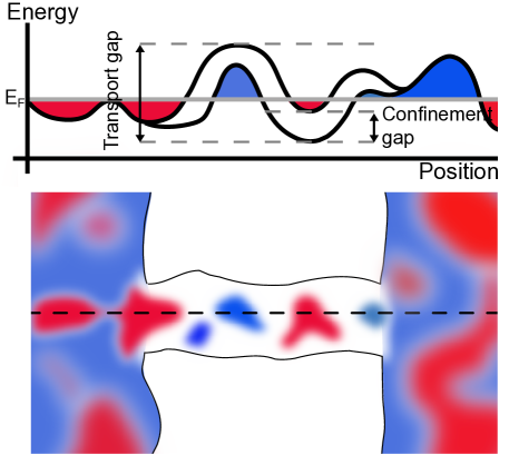
In the latter picture, in which potential inhomogeneities create a serial arrangement of quantum dots, we expect two distinct “gaps.” First, the quantum dot behavior is only apparent when the Fermi level is close enough to the charge neutrality point that the carrier density varies spatially from electron-like to hole-like (see Figure 1), since otherwise there will be no tunnel barriers between puddles to form quantum dots. Thus the transport gap (the region of suppressed conductance at zero bias) is given approximately by the disorder amplitude plus the confinement gap. The second gap is the “source-drain gap,” which is roughly the largest value of source-drain voltage for which conductance is suppressed at some . In the simplest case of single-dot transport, the source-drain gap is the charging energy of the dot, which need not have a clear dependence on the disorder amplitude. In the case of multiple quantum dots, determining the source-drain gap is more complicated, but we still expect the source-drain gap to depend on the particular shape of the disorder potential, and the shape of the disorder potential is not strongly constrained by its amplitude.
In this work, we present transport measurements on graphene nanoribbons of 30 nm width and lengths between 30 nm and 3 microns; we highlight several key features of our data that support the model of transport through quantum dots produced by charged impurities in the vicinity of the ribbon. First, by considering the effect of annealing nanoribbons to remove impurities from the surface of the ribbon, we show that the source-drain and transport gaps cannot be predicted on the basis of geometry alone: the gap properties appear to strongly depend on the particular arrangement of nearby impurities. Second, we show that the transport gap varies independently from the source-drain gap, in contrast with the findings of previous work.Molitor2009 The transport gap decreases with annealing, which we expect within the disorder-potential-induced quantum dot model since annealing should reduce the amplitude of the disorder potential. Third, similarly to the findings of studies on extended graphene sheets,Chen2008 we find a connection between the transport gap size and its distance from zero volts in back gate, suggesting that the transport gap is a measure of the doping of the sample; the doping is likely connected to the disorder amplitude. Fourth, we provide data on the relationship between source-drain gap and ribbon length: we find that in general longer ribbons have larger gaps, although the scatter in these data is substantial. Finally, we present measurements on a particular ribbon sample exhibiting very periodic conductance oscillations that suggest that the resonances commonly observed in nanoribbon measurements result from Coulomb blockade effects rather than Anderson localization effects.
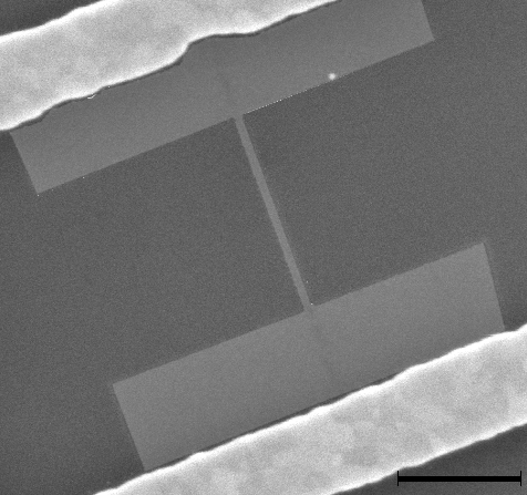
Our samples were fabricated with a metal etch mask technique, which allowed us to produce nanoribbons with an exposed surface for annealing experiments as well as a width that is consistent across samples (we estimate that each ribbon is of width 30 +/- 4 nm, with edge roughness less than 4 nm; the error bars are determined primarily by the resolution of the SEM used for imaging). First, graphene flakes were deposited on top of a 300-nm-thick layer of dry thermal oxide grown on a highly doped silicon substrate that serves as a back gate; flakes were identified optically and verified to be single layer by Raman spectroscopy.Ferrari2006 Gold contacts with a titanium sticking layer (15 nm Ti/45 nm Au) were then patterned to the flake by electron-beam lithography and electron-beam evaporation. A 30-nm-wide titanium line was patterned between contacts to define the ribbon, and a PMMA mask was used to cover regions near the contacts to preserve graphene leads at each end of the ribbon; the whole chip was then exposed to oxygen plasma (8 seconds at 65 W) to remove unmasked graphene. The titanium etch mask was washed away in a solution of 30% hydrochloric acid at 85∘C, and the PMMA mask on the leads was removed in acetone (the HCl penetrates under the PMMA mask so that parts of the titanium mask still covered by the PMMA are also removed). The resulting devices consist of metal contacts connected to graphene leads that in turn contact the nanoribbon. A typical device is shown in Figure 2.
Measurements were conducted in a cryostat in vacuum at 4.2-4.4 K or while immersed in liquid helium at 4.2 K unless stated otherwise. For ease of comparison to other work, we calculate transport gaps by the method introduced by Molitor et al.,Molitor2009 which involves fitting a line to the regions where conductance increases approximately linearly surrounding the region where the conductance reaches zero, and then finding the points where the fit extrapolates to zero conductance. We identify the “source-drain gap” by first smoothing the data using a 0.5 V window in back gate voltage. We then identify the source-drain gap as the largest source-drain voltage below which, for both positive and negative biases, the (smoothed) differential resistance exceeds 5 M for some back gate voltage. The smoothing step is included because there are often one or two outlying “spike” features for which the resistance exceeds 5 M over a range of source-drain voltages much larger than the typical “gap” source-drain voltage near the charge neutrality point; these features have a very small width in back gate voltage ( V) and are washed out by the smoothing. While it is possible to choose different and equally valid definitions of the transport and source-drain gaps, any one definition applied consistently across our data sets allows us to make meaningful statements about the variation of these quantities with ribbon geometry. Like Molitor et al.,Molitor2009 we find that the precise gap definitions used do not change the general features of the results.
| Data set | Annealing history |
|---|---|
| A | Not annealed; data taken while |
| immersed in liquid helium | |
| B | Not annealed; data taken while |
| immersed in liquid helium | |
| C1 | Not annealed; data taken while |
| immersed in liquid helium | |
| C2 | Removed from cryostat after C1, |
| argon annealed at 300∘C, | |
| exposed to atmosphere, cooled down; | |
| data taken in vacuum | |
| C3 | Warmed to RT after C2, current |
| annealed in vacuum at A/cm2, | |
| cooled down (without breaking vacuum | |
| since C2) | |
| D1 | Not annealed; data taken in vacuum |
| D2 | Exposed to atmosphere after D1, |
| current annealed in vacuum at | |
| A/cm2, cooled down; data taken in vacuum | |
| D3 | Warmed to RT after D2, current annealed |
| in vacuum at A/cm2, cooled down | |
| (without breaking vacuum since D2) | |
| E | Not annealed; data taken in vacuum |
We collected differential conductance data from several sets of ribbons before and after annealing. The details of the various data sets are shown in Table 1. We used two forms of annealing that have been reported to remove surface impurities in extended graphene sheets: annealing of the whole chip in argon at 300∘C,Elias2009 and current annealing in vacuum, which heats an individual ribbon by Joule heating.Moser2007 ; Bolotin2008 A representative set of results from our annealing experiments is shown in Figure 3. The first key feature of these data is that annealing tends to decrease the transport gap. We expect annealing both to remove impurities (such as resist residue or contaminants collected while the sample was exposed to the atmosphere) on the surface of the nanoribbon, and to rearrange impurities in the vicinity of the ribbon. If there were clusters of charged impurities with a dominant polarity distributed across the surface of the ribbon, we would expect the amplitude of the disorder potential created by the impurities to be reduced upon annealing, since the charge density in the clusters would be reduced. Reducing the disorder amplitude should reduce the region in where transport is suppressed (i.e., reduce the transport gap); the shrinking transport gap thus agrees with the model of quantum dots forming in the ribbon as a result of the disorder potential. However, we note that the shrinking transport gap can agree with any model in which annealing removes impurities that cause localization.
The second important result from Figure 3 is that the source-drain gap can change arbitrarily upon annealing. These unpredictable changes make sense within a quantum dot model; while annealing is expected to reduce the density of nearby charged impurities, it is also expected to rearrange those impurities that remain, resulting in a different configuration of charge puddles than that before annealing. Since the sizes and locations of the new puddles should be randomly distributed, the unpredictable changes of the source-drain gap are understandable: the source-drain gap is strongly dependent on the sizes of the dots and the coupling between them.
Were the observed conductance suppression caused primarily by localization due to edge roughness or defects in the lattice, we would not expect such dramatic changes in behavior upon annealing. Recent studies,CamposDelgado2009 in which chemically-grown graphene nanoribbons were annealed in argon for 30 minutes, have found correction of lattice point defects and edge reconstruction to occur only at temperatures near 1500∘C and above; our argon annealing experiments were carried out at 300∘C. Current annealing studiesJia2009 on chemically-grown nanoribbons also suggest that temperatures of over 2000∘C (perhaps near 2800∘C) must be achieved to reconstruct edges and improve the crystallinity of the sample by Joule heating. Since the SiO2 substrate that our ribbons sit on melts around 1650∘C, and since AFM and SEM measurements reveal no melting of the substrate after annealing, our ribbons likely do not reach the temperatures required to cause crystal reconstruction.
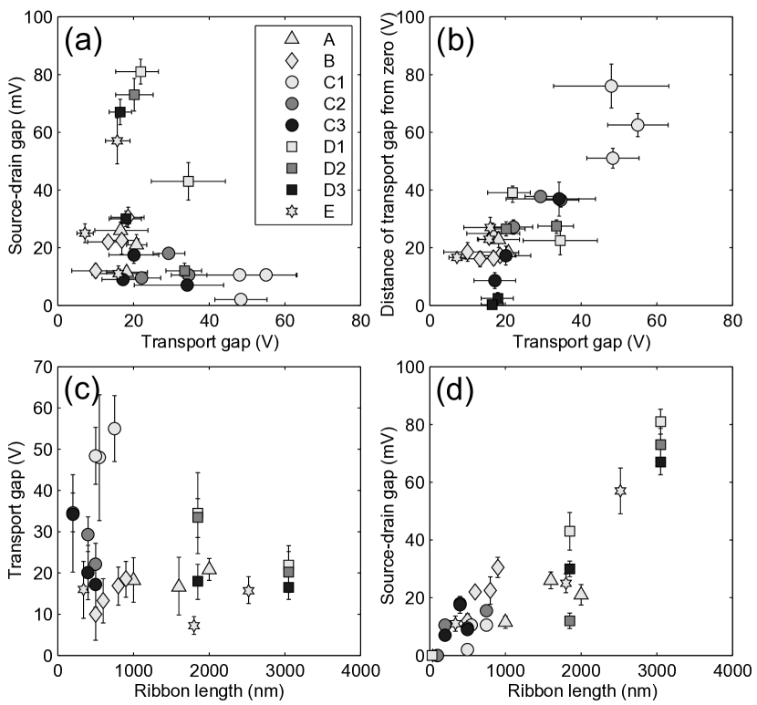
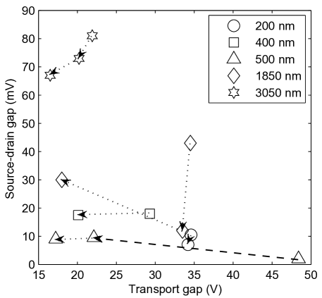
It has been suggested by Molitor et al. that the source-drain and transport gaps are related: in their six samples (widths 30 to 100 nm, lengths 100 to 500 nm) they noticed an apparently linear growth of the transport gap with the source-drain gap.Molitor2009 But in our experiments annealing can either increase or decrease the source-drain gap while generally shrinking the transport gap, so we conclude that these two gaps are not so simply related. In Figure 4a, we show the transport gap versus source-drain gap for our samples, in which there is no linear relationship between gaps. While it is possible that the two data sets reflect the same underlying physics, it is also possible that different physics may determine the behavior of their ribbons which are on average wider and are created via a different process, which could lead to a different degree of disorder. The lack of a simple relationship between the source-drain and transport gaps can be explained within the impurity-induced quantum dot picture: the source-drain gap is sensitive to the specifics of the potential landscape, but the disorder amplitude, which is roughly identified with the transport gap, does not strongly constrain the shapes and sizes of the puddles induced by the potential landscape.
In support of the suggestion that the transport gap is a measure of the amplitude of the disorder potential is our finding that, in addition to reducing the size of the transport gap, annealing tends to shift the center of the transport gap closer to zero volts in back gate. Assuming that one sign of charged impurity dominates, the distance of the charge neutrality point from zero gate voltage grows with the number of charged impurities, since these impurities dope the sample. Although this assumption need not be valid, in Figure 4b we find a common trend among our samples (annealed or not) that the magnitude of the transport gap increases as the distance of the center of the gap from zero in back gate voltage increases. This finding is reminiscent of the behavior of extended graphene samples upon dosing with charged impurities; experiment Chen2008 and theory Adam2007 indicate that the width of the conductivity minimum increases with the distance of the charge neutrality point from zero gate voltage because transport behavior in extended graphene sheets is governed by charged impurity scattering. While there remains some disagreement about the main scattering mechanism in graphene, our results are consistent with the charged impurity scattering model. We thus propose that in our samples there is a dominant sign of charged adsorbate before annealing (typically negative, since the charge neutrality point is usually at a positive gate voltage), and that the shifting of the charge neutrality point toward zero volts upon annealing results from the removal of charged impurities.
As shown in Figure 4c, the transport gap has little inherent length dependence, consistent with a simple link between transport gap and disorder amplitude. Certainly, for a short enough ribbon, there is no measurable gap, and our definition of the transport gap is meaningless. However, this was only the case for ribbons less than 200 nm long; for longer ribbons, the transport gap as defined does seem to primarily measure the disorder and not the ribbon length.
Although the transport gap evidently has little length dependence, the source-drain gap follows the general trend of increasing as a function of ribbon length (Figure 4d). The scatter in the data and limited number of data points prevent extraction of a quantitative trend; however, the scatter itself is consistent with the impurity disorder potential picture, in that the gap properties are sensitive to the particular potential profile in the ribbon. Importantly, much of the scatter is coming from different measurements on the same ribbon after different annealing procedures, so that slight lithographic differences between ribbons (e.g., different widths or edge details) cannot be primarily responsible for the scatter. We also point out that, on average, a longer ribbon would have more quantum dots whose energies need to be appropriately positioned with respect to the energies of their neighbors to enable transport; this would, on average, increase the bias voltage required to push electrons across the ribbon (i.e., increase the source-drain gap).
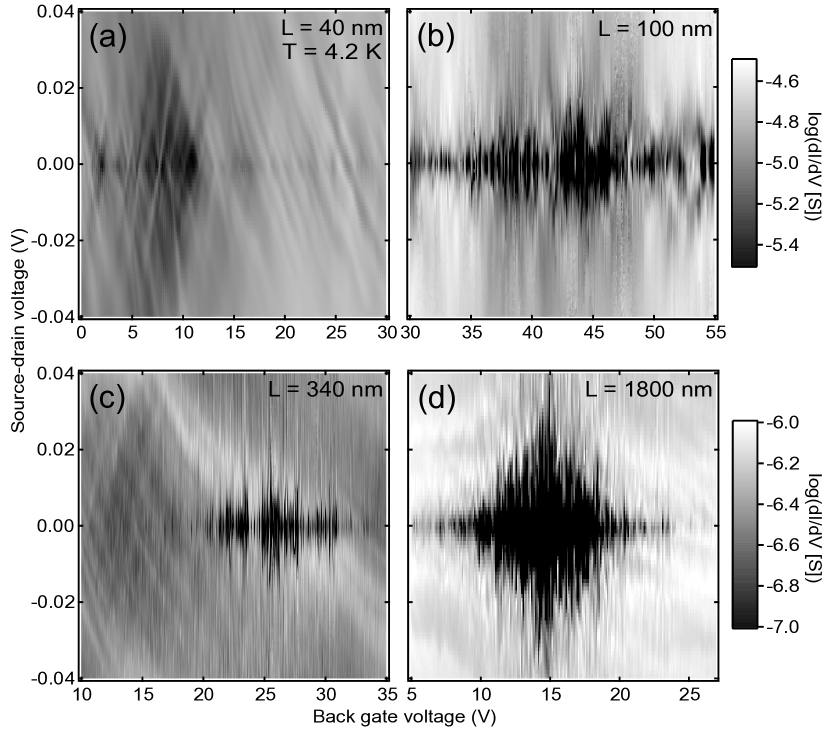
Another feature in Figure 4d is that our 30 and 40 nm-long ribbons had no regions of back gate voltage where conductance was low enough to be considered “gapped” per our definitions. On the other hand, our ribbons that were at least 100 nm long all had some gapped regions in gate voltage. Data illustrating the evolution of the gap for small ribbon lengths are shown in Figure 5. If transport is controlled by puddles of localized carriers surrounded by regions of zero carrier density, we expect there to be some length below which a puddle is too well-coupled to the leads to cause strong Coulomb blockade, and thus there will be no gap. Recent STM experiments indicate that charge puddles in extended graphene sheets at the charge-neutrality point have an average length-scale of about 20 nm. Zhang2009 Computational studies also suggest that the typical puddle size in graphene at the charge-neutrality point is on the order of 10 nm. Rossi2008 Although we do not know how this puddle size would be different in the case of nanoribbons, the largest ribbon length below which there is no gap is on the order of tens of nanometers for these 30-nm-wide ribbons; the lengthscales are thus consistent with the results of the STM experiments and simulations.

Along with the above aggregate results in support of the impurity disorder potential model, we have observed transport features in one particular ribbon that, after annealing, strongly resemble Coulomb blockade through one main quantum dot that may span much of the ribbon’s area. In Figure 6, we show a plot of conductance versus gate voltage from this sample. In the left inset of Figure 6, we show a closeup of a small range in back gate voltage from the same sweep; on this scale, very regular conductance peaks can be identified. Hundreds of such peaks occur over a range of more than 40 V in back gate with constant peak spacing. The peaks survive with the same periodicity on the rising background in the more heavily doped region of negative back gate voltage. As the back gate voltage is increased to about 15 V, the peaks become less periodic. The right inset of Figure 6 shows a closeup of part of the region in gate voltage where the behavior loses periodicity; while clusters of peaks can have the same peak spacing, there are a number of peaks at irregular positions.
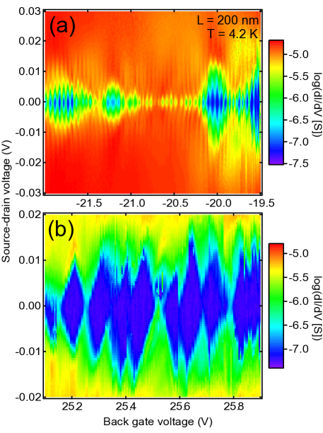
In plots of differential conductance versus bias and back gate voltage in the periodic region, such as that in Figure 7a, features that resemble the Coulomb diamonds of a single quantum dot are apparent. The heights of these diamonds are modulated as a function of gate voltage such that adjacent diamonds form diamond-like packets, suggesting the presence of another physically smaller quantum dot that is strongly coupled to a lead and is acting in series with the larger quantum dot responsible for the smaller diamonds. In contrast, Figure 7b shows the less periodic region, in which we find “overlapping” diamond features characteristic of Coulomb blockade effects in a serial arrangement of multiple weakly coupled quantum dots.
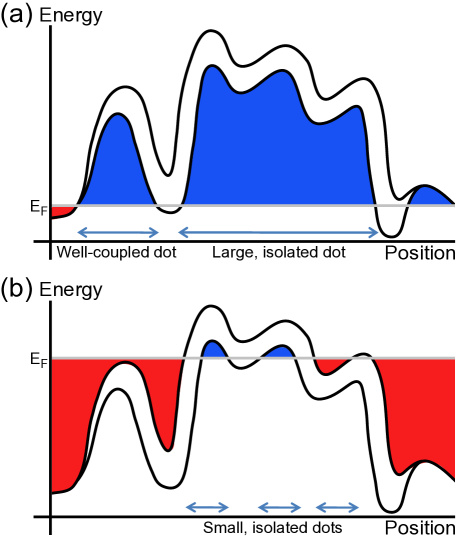
The transition from periodic to less periodic behavior as the Fermi level is moved through the transport gap is suggestive of Coulomb blockade occuring due to potential inhomogeneities. In Figure 8a, we show a cartoon representation of a potential profile, composed of one large “well” with some weaker modulation inside the well, which could give rise to the observed phenomena. For some range of that includes the shown in Figure 8a, there is only one isolated puddle, which spans most of the ribbon. There is also a smaller puddle that is strongly coupled to one lead. But when is in the range of the weaker modulation inside the well (Figure 8b) the ribbon splits up into more than one isolated puddle; this is a serial arrangement of multiple weakly tunnel-coupled quantum dots.
We note that it is possible that the larger, more isolated quantum dot that exists in the periodic region of gate voltage does not span as much of the ribbon as we have shown in Figure 8a. However, if the dot takes up only a fraction of the ribbon, the potential must be exceptionally smooth; any substantial roughness will create other isolated quantum dots near where the disorder potential energy crosses the Fermi level. Since our system apparently only has one isolated dot, and since an extremely smooth disorder potential seems unlikely, we propose that the isolated quantum dot does span most of the ribbon.
To quantitatively estimate the dot size, we use the peak spacing ( V) along with the capacitance per unit length calculated by Lin et al.Lin2008 ( 3.5 10 F/nm) for a graphene nanoribbon of 30 nm width above 300 nm of SiO2. We find a dot area of 3000 nm2, which corresponds to a 100 nm-long dot if the dot spans the width of the ribbon. This agrees with our qualitative argument that the main dot covers most of the ribbon.
We think it unlikely that the dot in this ribbon is nucleated by a single impurity. Based on the mobilities of our devices measured outside the ribbon body, following earlier models Chen2008 we estimate the density of charged impurites near the graphene sheet to be before annealing. Studies Chen20082 on extended graphene flakes have suggested that the maximum achieveable mobilities for graphene on SiO are limited to 15,000 cm/Vs, corresponding to an impurity density of roughly . Even if we were to achieve this maximum mobility after several annealing attempts, we would still expect more than one impurity within the area of this ribbon. Since clustering of impurities and overscreening effects are likely, we do not expect a one to one correspondence between impurities and charge puddles.
Importantly, the gradual transition from periodic to aperiodic behavior observed in Figures 6 and 7 suggests that the less periodic peaks are also Coulomb blockade peaks. These conductance peaks in the less periodic region are similar in width and lineshape to those in our other ribbons that exhibit little periodic behavior; given this point, Coulomb blockade phenomena are likely being observed in our other ribbon samples as well. While it has been proposed that Anderson localization can create conductance peaks and transport gap phenomena,Mucciolo2009 peaks created by Anderson localization would not occur with highly periodic spacing over a wide range of Fermi energies.
In summary, we have provided evidence in support of a model of nanoribbon behavior in which charged impurities in the vicinity of the ribbon create a disorder potential that, coupled with some small energy gap, breaks the ribbon up into isolated puddles of charge carriers that act as quantum dots. By performing annealing studies on our nanoribbons, we have demonstrated that the source-drain and transport gaps are distinct quantities, as expected within the quantum dot model. Our data further imply that the transport gap reflects the doping of the sample as well as its disorder amplitude, suggesting that the gap phenomena arise in large part from disorder due to charged impurities. We showed that the source-drain gap is not a simple function of ribbon length and width, but that it seems to depend sensitively on the potential profile in the nanoribbon; this result is understandable within the quantum dot framework since the dots’ sizes, positions, and tunnel barriers are controlled by the precise potential profile, and the transport properties of a system of quantum dots depend heavily on these parameters. Nonetheless, longer ribbons tend to have larger source-drain gaps, and very short ribbons exhibit no gap behavior; this behavior is understood within our model, since there is some smallest length required to fit a well-isolated quantum dot in the ribbon to block transport, and since a longer ribbon will on average have more quantum dots that electrons must tunnel across for conduction, increasing the source-drain gap. Finally, we provided data from a 200 nm long ribbon displaying highly periodic modulations of conductance versus gate voltage; we have identified these modulations as Coulomb blockade oscillations based on their similarity to Coulomb oscillations in single-quantum dot systems. This supports the idea that the conductance peaks commonly observed in nanoribbons arise from Coulomb blockade rather than from Anderson localization due to edge disorder.
The apparent importance of disorder in determining transport properties of lithographically-defined graphene nanoribbons raises questions about the feasibility of using such ribbons as next-generation transistor technology. We acknowledge that the influence of disorder due to charged impurities near the ribbon relative to the influence of atomic-scale disorder at the ribbon edges may differ in ribbons fabricated by different techniques. This variation may occur even in ribbons lithographically fabricated via differing masking techniques. More radically, new methods have been proposed for making nanoribbons with atomically ordered edges.Li2008 ; Jiao2009 However, we believe that our results demonstrate that unless the strength of disorder due to charged impurities near the ribbon can also be reduced (for instance, by suspendingBolotin2008 the nanoribbons), the transport behavior of these clean-edged nanoribbons will still be dominated by the Coulomb blockade of multiple quantum dots. But perhaps, by carefully controlling the amount of disorder in these ribbons, Coulomb blockade effects could be harnessed to create reliable switching behavior.
Acknowledgements.
We thank Gil Refael, Antonio Castro Neto, Eduardo Mucciolo, Misha Fogler, Enrico Rossi, Shaffique Adam, Stephan Roche, Sami Amasha, and Jimmy Williams for very useful discussions. We also thank Emerson Glassey for assistance with sample fabrication. This work was supported by the Center for Probing the Nanoscale, an NSF Nanoscale Science and Engineering Center, award PHY-0830228, through a Supplementary award from the NSF and the NRI; as well as by the Focus Center Research Program’s Center on Functional Engineered Nano Architectonics (FENA). P. Gallagher acknowledges support from the Stanford Vice Provost for Undergraduate Education. K. Todd acknowledges support from the Intel and Hertz Foundations. D. Goldhaber-Gordon acknowledges support from Stanford under the Hellman Faculty Scholar program. Work was performed in part at the Stanford Nanofabrication Facility (a member of the National Nanotechnology Infrastructure Network), which is supported by the National Science Foundation under Grant ECS-9731293, its lab members, and the industrial members of the Stanford Center for Integrated Systems.References
- (1) A. H. Castro Neto et al., Rev. Mod. Phys. 81, 109 (2009).
- (2) M. Y. Han, B. Özyilmaz, Y. Zhang, and P. Kim, Phys. Rev. Lett. 98, 206805 (2007).
- (3) Z. Chen, Y.-M. Lin, M. J. Rooks, and P. Avouris, Physica E 40, 228 (2007).
- (4) L. Brey and H. A. Fertig, Phys. Rev. B 73, 235411 (2006).
- (5) M. Ezawa, Phys. Rev. B 73, 045432 (2006).
- (6) L. Yang et al., Phys. Rev. Lett. 99, 186801 (2007).
- (7) K. Todd, H.-T. Chou, S. Amasha, and D. Goldhaber-Gordon, Nano Lett. 9, 416 (2009).
- (8) F. Molitor et al., Phys. Rev. B 79, 075426 (2009).
- (9) M. Evaldsson, I. V. Zozoulenko, H. Xu, and T. Heinzel, Phys. Rev. B 78, 161407(R) (2008).
- (10) E. R. Mucciolo, A. H. Castro Neto, and C. H. Lewenkopf, Phys. Rev. B 79, 075407 (2009).
- (11) C. Stampfer et al., Phys. Rev. Lett. 102, 056403 (2009).
- (12) X. Liu, J. B. Oostinga, A. F. Morpurgo, and L. M. K. Vandersypen, Phys. Rev. B 80, 121407(R) (2009).
- (13) F. Sols, F. Guinea, and A. H. Castro Neto, Phys. Rev. Lett. 99, 166803 (2007).
- (14) K. Nomura and A. H. MacDonald, Phys. Rev. Lett. 98, 076602 (2007).
- (15) K. Nomura, M. Koshino, and S. Ryu, Phys. Rev. Lett. 99, 146806 (2007).
- (16) J. H. Bardarson, J. Tworzydło, P. W. Brouwer, and C. W. J. Beenakker, Phys. Rev. Lett. 99, 106801 (2007).
- (17) J.-H. Chen et al., Nat. Phys. 4, 377 (2008).
- (18) We consider the question of whether all traces of the titanium mask are removed in the acid solution. It appears that residual titanium is not affecting transport properties, since the ribbons made by this process behave similarly to those made by other processes. Additionally, we prepared a test bulk sample by coating part of it in titanium and then etching away the titanium using the same process as was used for the nanoribbons. Four-wire conductance measurements revealed characteristic graphene behavior before the titanium etch mask was deposited and after it was removed, with a mobility degradation of the degree expected from additional lithography: the mobility decreased from 6000 cm2V-1s-1 to 800 cm2V-1s-1 after titanium deposition and removal. A bulk mobility of 800 cm2V-1s-1 is typical for the nanoribbon devices that we have fabricated in the past using two steps of lithography with no titanium deposition or titanium etch.Todd2009 Raman spectroscopy revealed no changes in the disorder peak after the titanium deposition and removal, and the Raman spectrum did not reveal any differences between the parts of the flake that were once covered with titanium and the parts that were not covered with titanium. Auger measurements from a PHI 700 found no residual titanium to within the sensitivity of the instrument: the titanium signal was the same on all parts of the devices studied, regardless of whether or not titanium had been deposited there to begin with. Based on Auger measurements of a titanium film of known thickness, we estimate that any residual titanium film on our nanoribbons is less than 0.2 nm thick. While this upper bound is rather large, based on all the evidence presented here, we feel that the titanium mask is being sufficiently removed by our etch process and that the amount of residual titanium on our ribbons is much smaller than this upper bound.
- (19) A. C. Ferrari et al., Phys. Rev. Lett. 97, 187401 (2006).
- (20) J. Moser, A. Barreiro, and A. Bachtold, App. Phys. Lett. 91, 163513 (2007).
- (21) D. C. Elias et al., Science 323, 610 (2009).
- (22) K. I. Bolotin et al., Solid State Commun. 146, 351 (2008).
- (23) J. Campos-Delgado et al., Chem. Phys. Lett. 469, 177 (2009).
- (24) X. Jia et al., Science 323, 1701 (2009).
- (25) S. Adam, E. H. Hwang, V. M. Galitski, and S. Das Sarma, PNAS 104, 18392 (2007).
- (26) W. Liang et al., Nature 411, 665 (2001).
- (27) Y. Zhang et al., Nat. Phys. 5, 722 (2009).
- (28) E. Rossi and S. Das Sarma, Phys. Rev. Lett. 101, 166803 (2008).
- (29) W. G. van der Wiel et al., Rev. of Mod. Phys. 75, 1 (2002).
- (30) Y.-M. Lin, V. Perebeinos, Z. Chen, and P. Avouris, Phys. Rev. B78, 161409(R) (2008).
- (31) J.-H. Chen et al., Nat. Nanotechnol. 3, 206 (2008).
- (32) X. Li et al., Science 319, 1229 (2008).
- (33) L. Jiao et al., Nature 458, 877 (2009).