Crossed Andreev reflection versus electron transfer in graphene nanoribbons
Abstract
We investigate the transport properties of three-terminal graphene devices, where one terminal is superconducting and two are normal metals. The terminals are connected by nanoribbons. Electron transfer (ET) and crossed Andreev reflection (CAR) are identified via the non-local signal between the two normal terminals. Analytical expressions for ET and CAR in symmetric devices are found. We compute ET and CAR numerically for asymmetric devices. ET dominates CAR in symmetric devices, but CAR can dominate ET in asymmetric devices, where only the zero-energy modes of the zigzag nanoribbons contribute to the transport.
pacs:
74.45.+c, 73.63.-b, 73.23.-b, 74.25.FyI Introduction
Graphene, a two-dimensional honeycomb lattice of carbon atoms, has recently been experimentally realized.Novoselov et al. (2004); Zhang et al. (2005); Novoselov et al. (2005) It exhibits intriguing electron transport properties such as a very high mobility,Novoselov et al. (2004); Zhang et al. (2005); Novoselov et al. (2005) gate-voltage tunable electron doping,Novoselov et al. (2004) anomalous quantum Hall effect,Zhang et al. (2005) Klein tunneling,Katsnelson et al. (2006) “relativistic” Dirac-like linear energy-momentum dispersion,Semenoff (1984) and possible integration with other adatoms and electrical contacts.Geim and Novoselov (2007); Neto et al. (2009) Graphene can be contacted to superconductors and a supercurrent in graphene Josephson junctions has been measured.Heersche et al. (2007); Du et al. (2008); Kessler et al. (2010)
Non-local transport in three-terminal devices with one superconducting lead and two normal metals has been extensively studied, both theoreticallyByers and Flatté (1995); Deutscher and Feinberg (2000); Falci et al. (2001); Bignon et al. (2004); Morten et al. (2006, 2008) and experimentally.Beckmann et al. (2004); Russo et al. (2005); Cadden-Zimansky and Chandrasekhar (2006); Kleine et al. (2009) At energies lower than the superconducting gap, the current in one normal terminal caused by a voltage applied between another normal terminal and the superconductor is governed by a competition between electron transfer (ET) and crossed Andreev reflection (CAR). ET is the emission of an electron from one normal metal terminal to another normal metal terminal, possibly after interacting with the superconductor. In CAR, an electron from one normal terminal enters the superconductor together with an electron from a second normal terminal or, equivalently, an electron is emitted into one normal terminal while a hole is emitted into another normal terminal. This process creates a spatially entangled electron-hole pair which has a fundamental interest and can be used as an entangler.Recher et al. (2001); Chtchelkatchev et al. (2002); Recher and Loss (2003) The relative magnitude of ET and CAR can be tuned by using ferromagnetic contacts,Falci et al. (2001); Mélin (2001) but our focus here is on their intrinsic relative value when normal metals are used. The ET and CAR processes contribute with opposite signs to the non-local current. Experimentally, it has been measured that ET often dominates CAR, but at finite bias voltage a CAR dominated signalRusso et al. (2005) was also seen. First theories in the lowest order tunneling limit predict that ET and CAR exactly cancel each other.Falci et al. (2001) Also, relaxing the assumption of tunneling barriers by allowing barriers of arbitrary strength in semi-classical N-S circuits, ET generally dominates CAR.Morten et al. (2006) Recent theoretical suggestions to explain the experiment in Ref. Russo et al., 2005 are Coulomb interaction effects,Levy Yeyati et al. (2007) an external AC bias,Golubev and Zaikin (2009) and quantum interference effects.Golubev et al. (2009)
Theoretically, graphene-superconductor junctions have been investigated by several workers. Beenakker (2006); Titov and Beenakker (2006); Burset et al. (2008) In graphene there is an additional new quasi-particle to supercurrent conversion process denoted specular Andreev reflection, where states above and below the Dirac point are coupled by Andreev scattering (inter-band coupling).Beenakker (2006) In specular Andreev reflection, the holes emitted from the superconductor no longer follow the parallel time-reversed path of the incoming electron as they do in direct Andreev reflection, but are specularly reflected at an angle which equals the angle of incidence. Although fundamentally interesting, as it could enhance CAR processes,Benjamin and Pachos (2008); Cayssol (2008) specular Andreev reflection is only visible in ultra clean and homogeneous systems, since the Dirac point must be well-defined throughout the region of interest, or the superconducting pair potential must be much larger than the typical variation in the Dirac point. Also, it is necessary to control the doping such that the Fermi energy is considerably smaller than the superconducting gap. The small magnitude of the proximity induced superconducting gap in graphene, ,Heersche et al. (2007) means this could only be realized in ultra small structures at very low doping level in well controlled systems.
In this paper we investigate the influence of a superconducting terminal on devices built from graphene zigzag ribbons. We are interested in studying how ET and CAR depend on the features of the nanoribbons e.g. on their widths, number of terminals, and relative angle where ribbons connected to various terminals intersect. The choice of zigzag ribbons is the most relevant one, as the boundary conditions for ribbons with generic boundaries have been shown to reduce to the boundary conditions for zigzag terminations in most cases.Akhmerov and Beenakker (2008); Rycerz (2008) Such nanoribbons have some unique electronic features, such as supporting current carrying zero-modes localized along the edges.Fujita et al. (1996); Nakada et al. (1996); Rycerz (2008) Also, for low energies, states carrying current in opposite directions along the zigzag ribbon is associated with different eigenstates, and there is an absence of backscattering due to the small overlap between the states carrying current in opposite directions.Rainis et al. (2009)
The paper is organized as follows: In Sec. II we define our model and in Sec. III we express the scattering matrix in terms of the normal state scattering matrix. This enables us to identify the ET and CAR contributions to the non-local signal. Section IV describes the properties of symmetric three-terminal devices, and in Sec. VI we present numerical results showing a dominance of CAR over ET in an asymmetric device. Finally we conclude our paper in Sec. VII.
II Model and method
Our description of superconducting ribbons starts with the nearest neighbor hopping Hamiltonian of graphene,
| (1) |
where is the nearest neighbor hopping energy, Wallace (1947); Reich et al. (2002); Neto et al. (2009) and creates an electron with spin at site . In the superconducting terminal, we assume a superconductor on top of the graphene sheet which by proximity induces superconducting properties in graphene. We consider spin singlet pairing described by the BCS Hamiltonian .Bardeen et al. (1957) The superconducting pair potential is local to site and chosen to be real since we only have one superconductor. We write in Nambu form,
| (2) |
where and are elements of the normal state Hamiltonian in Eq. (1).
We are interested in the transport properties which can be expressed via the scattering matrix of the system. Following Ref. Büttiker, 1992, we find that the differential conductance matrix isBlonder et al. (1982)
| (3) |
where is the number of propagating modes in lead at energy , and the conductance matrix elements are defined in terms of the Nambu space scattering matrix
| (4) |
as
| (5) | ||||
| (6) | ||||
| (7) | ||||
| (8) |
The conductances in Eqs. (5) – (8) describe, respectively, local electron reflection (ER), direct Andreev reflection (DAR), non-local electron transfer (ET), and crossed Andreev reflection (CAR).
All energies are measured with respect to the equilibrium chemical potential of the superconductor, and all conductances in this paper are in units of two times (for spin) the conductance quantum . The current is defined as incoming from reservoir .
III Scattering matrix of a three-terminal device with one superconducting terminal
In the following we will study the non-local signal in a three-terminal device, where terminal 1 is superconducting and terminals 2 and 3 are normal metals. The non-local conductanceFalci et al. (2001); Morten et al. (2006)
| (9) |
is positive when dominated by ET and negative when dominated by CAR.
We compute and in two ways: i) and are computed directly in Nambu space using the Hamiltonian (2), and and are found from (7) and (8). We refer to this as the Nambu approach. ii) We relate and to the scattering matrix in the normal state and numerically compute the latter using the Hamiltonian (1). We call this the Normal approach. Our results using both methods agree, when applicable. Let us first review how the scattering matrix can be related to the normal state properties.
Following Ref. Beenakker, 1992, if the scattering region is well separated from the superconducting terminal, we can express the scattering matrix when terminal 1 is superconducting in terms of the scattering matrix
| (10) |
when the whole device is in the normal state. As long as the device is appreciably smaller than the superconducting coherence length , the normal approach is applicable. For graphene, the induced superconducting gap is small, ,Heersche et al. (2007) so that the coherence length is on the order of micrometers.
With terminal 1 superconducting, the scattering matrix between the normal metal terminals and isBeenakker (1992); Lesovik et al. (1997)
| (11) | ||||
| (12) |
where the matrix is
| (13) |
The amplitude , associated with electron-hole conversion at the normal-superconducting interface, isLesovik et al. (1997)
| (14) |
and the bar () corresponds to time reversal, defined for an arbitrary quantity as:
| (15) |
The matrix corresponds to all orders of the process where a hole emitted from the superconductor returns to the superconductor. At zero energy, holes propagating with amplitude between successive interactions with the superconductor retrace exactly the reverse path of the electrons with amplitude . Thus, at zero energy holes and electrons do not acquire a phase relative to each other upon interacting with the scattering region. However, at non-zero energy, there is a mismatch between the wave vectors of electron-like and hole-like states, so the time reverse paths described by the scattering matrices and will not be exactly opposite to each other. This means that the term in contains many different phases, which will depend strongly on the disorder configuration. There is therefore some loss of coherence at non-zero energy due to phase randomization.
For the ET process, described by the scattering matrix element in Eq. (11), there is an interference of two types of processes: (1) Going directly from to without interacting with the superconductor, and (2) processes involving any number of electron-hole-electron conversions at the interface to the superconductor. Similarly, the Andreev process described by Eq. (12) involves an odd number of electron-hole conversions at the NS interface.
In the absence of a magnetic field, time-reversal symmetry dictates Datta (1995)
| (16) |
The energy scale of the normal state scattering matrix is the subband energy, which is determined by the hopping energy and the width of the ribbon. For the ribbons considered in this paper, the subband energy is larger than the superconducting pair potential by several orders of magnitude. The Fermi energy is comparable to the subband energies in magnitude. Since, in the regime we consider, is independent of energy on the scale of , we write and .
The non-local ET and CAR conductances therefore simplify to
| (17) | ||||
| (18) | ||||
where all energy dependence is due to the electron-hole conversion amplitude .
When , Eq. (14) gives , and we recover the normal state behavior where only the first term of Eq. (17) contributes. However, in the subgap limit , , and the interaction with the superconductor contributes. The second term in Eq. (17) is due to interference between processes involving direct transfer of electrons from 2 to 3, and interaction with the superconducting terminal 1.
In our numerical studies, we calculate the retarded Green’s function matrix and extract the elements involving the terminals and . The calculation of uses the recursive method described in Ref. Kazymyrenko and Waintal, 2008. In this method, the Green’s function of the whole system is found by adding the sites of the Hamiltonian (1) to the system one by one, updating all relevant Green’s function elements via the Dyson equation. The method has the advantage that it can easily be applied to structures of arbitrary geometry and any number of terminals. After the Green’s function has been found, the scattering matrix is extracted via the Fischer-Lee relations,Fisher and Lee (1981); Datta (1995)
| (19) |
Here is the identity matrix (operator) and is the linewidth/dephasing matrix which depends on the self energy of terminal .
IV Symmetric three-terminal device
The simplest three-terminal device is completely symmetric where the normal state scattering matrix (10), simplifies to
| (20) |
Unitarity of gives rise to the relations
| (21) | ||||
| (22) |
that we make use of in Eqs. (17) and (18) to find the non-local conductance. We can express the conductance matrix of such a symmetric device in terms of the eigenvalues of the reflection probability matrix :
| (23) | ||||
| (24) |
It follows from this that the non-local conductance of a symmetric structure,
| (25) |
is always ET dominated (positive). By a completely analogous calculation we also find that the local conductance,
| (26) |
is naturally also positive.
A few simple conclusions can be drawn from these expressions. First, when the device is perfectly transparent for the contributing modes at the Fermi energy, the contributing modes have , the others have . The local and non-local conductances become,
| (27) | ||||
| (28) |
where is the number of modes contributing to the current at the Fermi energy. These results have the following simple explanation: When the voltage is raised in terminal 2, conducting modes are injected into the structure via this terminal. Since the device is symmetric, half of these modes go directly to terminal 3, producing a current in this terminal. The other half of the incoming modes interact with the superconductor at terminal 1, and are Andreev reflected back to terminal 2 as holes. These modes contribute to the current in terminal 2. The total current in terminal 2 is therefore . At low bias the Andreev reflected holes retrace exactly the trajectory of the incoming electrons because of time-reversal symmetry, and they therefore only contribute to the current in terminal 2.
When all the terminals are connected to the central device with tunnel contacts, we can expand the local and non-local conductances in the for the contributing modes. We find that
| (29) | ||||
| (30) |
so we recover the normal state results, where both the local and non-local signals vanish linearly with . Transport between terminals 2 and 3 involving the superconductor involves higher orders in and does therefore not contribute in this limit.
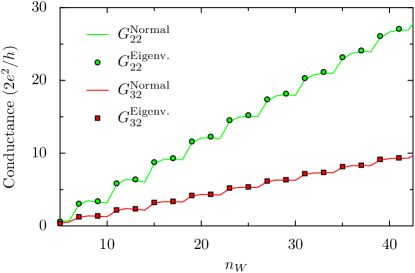
We check the consistency between the eigenvalue expressions (25) and (26) and our numerical routines by calculating the local and non-local conductances and in a symmetric three-terminal graphene device, as explained further in Sec. V. As can be seen from Fig. 1, where the conductances are plotted as a function of the width of the nanoribbons, we have excellent agreement between the eigenvalue expressions (symbols) and the results found directly from Eq. (3) (lines). Note that Eq. (3) is valid for any width , while only even give a truly symmetric device when built from zigzag nanoribbons, so only such data points are shown. However, we find that the results found from (ab-)using the eigenvalue expressions when is odd are also very close to the numerical results. This is not surprising, since as long as many modes contribute to the current, small alterations of the geometry should not have a big impact on the total current.
V Asymmetric three-terminal device
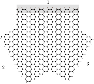
Having found that ET dominates non-local transport in a symmetric device, we turn our investigation to asymmetric devices. We do this numerically, by calculating the scattering matrix in a three-terminal device obtained by joining three semi-infinite zigzag graphene nanoribbons as shown in Fig. 2.
The width of a zigzag graphene nanoribbon, , is determined by the minimal number of bonds that must be broken to cut the ribbon.Fujita et al. (1996) is the lattice constant of graphene, .Wallace (1947)
For a wide ribbon, , the energy of the ’th transverse subband is to a good approximationRycerz et al. (2007)
| (31) |
where is the nearest neighbor hopping energy on the graphene lattice. The superconducting coherence length
| (32) |
will typically be of the order of micrometers, so the normal approach should be applicable for nanoribbons up to wide, or .
V.1 Consistency checks
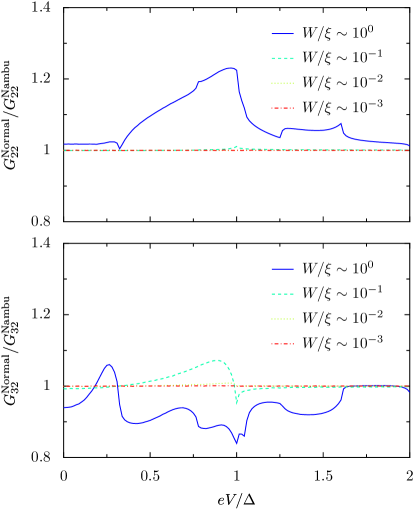
In Fig. 3 we compare the conductance extracted from the normal state scattering matrix to that found by direct evaluation of the full scattering matrix in Nambu space. The calculations are done for a device of the type shown in Fig. 2. The leads are all semi-infinite zigzag ribbons, and we set everywhere except in terminal 1 (shaded area in Fig. 2). As can be seen from Fig. 3, where we show the ratio between the conductance calculated with the two methods, , the agreement between the two methods is excellent as long as , where is the width of the ribbons and is the superconducting coherence length.
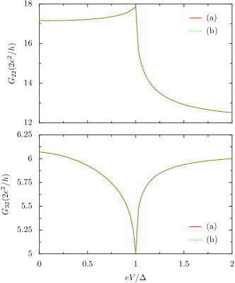
Also, since , the exact position of the boundary between the normal () and superconducting () regions does not influence our results. This can be seen explicitly from Figs. 4a and 4b, where we compare the conductance matrices for systems when the scattering region is, respectively, entirely mixed with, or separated from, the superconducting region. There is no dependence on the exact position of the NS interface, as should be expected.


V.2 Varying the width of the superconductor
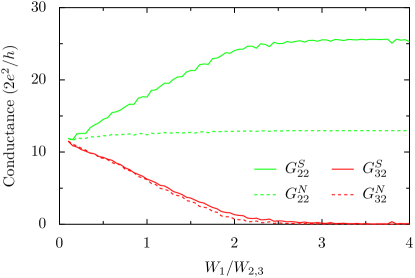
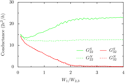
We now turn to the numerical calculations of the local and non-local conductances for an asymmetric device. We first vary the width of the superconducting lead, keeping the width of the normal terminals fixed, . The doping throughout the device is set to a high value to ensure that many modes contribute to the transport. The conductances involving the normal terminals are calculated when the top terminal is superconducting (superscript ), and compared for reference to the conductance when the whole device is in the normal state (superscript ). As seen in Fig. 5, when the superconducting lead is very narrow, there is very little coupling via the induced superconducting order parameter, so . However, as the width of the superconducting lead increases, more of the incoming quasiparticles are coupled via the induced superconducting order parameter, and the local conductance asymptotically approaches twice the normal state conductance, . In other words, the interaction with the superconductor essentially involves all the incoming modes, which are therefore Andreev reflected. This resembles the situation in a strongly coupled two-terminal NS junction.Beenakker (1992) From Fig. 5 we see that the contribution of Andreev reflection to the local conductance has reached its asymptotic value when .
The picture is essentially unchanged if we allow for different doping levels in the central device and the terminals (see Fig. 5b), as long as the number of contributing modes in the central region is still large.
Contrary to what is seen for the local conductance, the non-local conductance is only weakly influenced by the presence of the superconductor. Except for a slight enhancement of the signal around , the non-local conductance remains essentially unchanged when turning on the superconductor. This is in accordance with what was found for the symmetric device in Sec. IV, namely that the Andreev reflected holes retrace the path of the incoming electrons, giving a negligible contribution to the non-local conductance. Again, different doping levels in the central device and the terminals do not change the picture qualitatively, as seen from Fig. 5b.
V.3 Varying the width of normal terminal 3
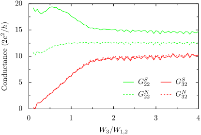
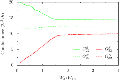
We also vary the width of the normal terminal 3, keeping the widths of the voltage terminal 2 and the superconducting terminal 1 fixed. As can be seen from Fig. 6 the non-local conductance, , is (nearly) zero when terminal 3 is very narrow. This is natural, since the subband energies in terminal 3 increase as the terminal is made narrower, hindering any modes from carrying current at the Fermi energy. As the normal lead 3 widens, more and more channels in this lead are opened, and we get an increase in the conductance due to the opening of new subbands. The current in terminal 3 saturates when all available subbands participate in the transport. We observe that the superconductor has very little influence on the non-local conductance. As in Sec. V.2, these results persist if we allow for different doping levels in the central device and the terminals, demonstrating the robustness of the results.
In contrast to the non-local conductance , the local conductance is strongly affected by the superconductor. doubles compared to the normal state value when the other normal lead becomes vanishingly small, . This is as expected, since we are effectively left with a strongly coupled two-terminal NS junction involving only normal terminal 2 and superconducting terminal 1. In the opposite limit, when , the ratio approaches an asymptotic value due to the fact that only a certain fraction of the finite number of incoming modes still interact with the superconductor, although the majority of these incoming modes are transferred directly to terminal 3 in this limit.
VI Non-local conductance dominated by CAR
VI.1 Zero modes of zigzag nanoribbons
A zigzag graphene ribbon supports special current carrying zero energy modes. When the doping is low (close to the Dirac point), the density of the zero energy modes is localized along the ribbon edges,Fujita et al. (1996); Nakada et al. (1996) while the current is distributed approximately uniformly across the width of the ribbon.Muñoz Rojas et al. (2006); Zarbo and Nikolic (2007); Nakakura et al. (2009) Associated with the zero energy modes is a quantum number called pseudoparity, arising from the fact that the unit cell of the honeycomb lattice contains two atoms.Akhmerov et al. (2008); Cresti et al. (2008); Rainis et al. (2009) The conservation of pseudoparity in a zigzag ribbon has dramatic consequences for the transport in a normal-superconducting (NS) junction when only the zero modes contribute, i.e. for Fermi energies below the first subband energy . In this regime each lead only supports one incoming and one outgoing mode. These two modes have either the same or opposite pseudoparities, depending on whether is even or odd, respectively.Rainis et al. (2009) As a consequence of this, in a zigzag ribbon NS junction, either normal reflection or direct Andreev reflection will be entirely suppressed, depending on the value of (modulo 2).Rainis et al. (2009) In a three-terminal device, pseudoparity is not a good quantum number, but when the transport involves only the zero modes, traces of even/odd effects can still be seen in the contributions due to Andreev reflection.
VI.2 CAR dominance
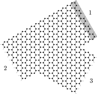
Motivated by the results of Refs. Rycerz and Beenakker, 2007; Iyengar et al., 2008; Katsnelson and Guinea, 2008, where it was found that a kink in a graphene ribbon can in certain situations completely block the electron flow, we construct a device as depicted in Fig. 7, consisting of a zigzag ribbon with a third terminal protruding at an angle of . The top terminal (1) is superconducting, while the left (2) and lower right (3) terminals are normal. We define and and set in this section. The superconductor is heavily doped, while the doping in the non-superconducting part of the structure is kept close to the Dirac point. We study the transport properties as a function of back gate voltage , which specifies the overall doping of the device, in the regime where only the zero modes contribute in the normal part of the device, .
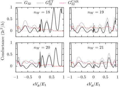
The numerical results in Fig. 8 show that the zero bias non-local conductance changes sign several times in the regime . This demonstrates that CAR can in principle dominate ET in rather specific geometries. The non-local conductance changes sign due to close competition between ET and CAR. The oscillatory pattern is determined by the distance between the superconducting terminal and the scattering centre at the junction between the ribbon and terminal 3. The contribution from Andreev reflection is insensitive to this length, as seen from Fig. 8. Also, we observe that when , a new subband starts contributing to ET, while CAR remains approximately unchanged.
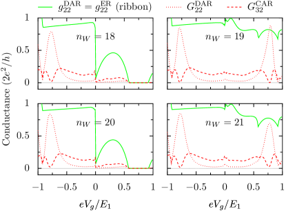
Finally, we also make a short comment on the even/odd behavour of our three-terminal device. By comparing our results with the conductance in a two terminal NS ribbon (similar to the device in Fig. 7, but without terminal 3), we see that the even/odd behaviour of is reflected in and , as can be seen from Fig. 9. According to the results of Ref. Rainis et al., 2009, incoming carriers at positive and negative have opposite (identical) pseudoparities in a ribbon with even (odd). With our chosen doping in the superconductor, this leads to a blocking of Andreev reflection for positive in the two-terminal ribbon (solid green line) when is even. This feature is still manifest in the local DAR (dotted red line) and non-local CAR (dashed red line) contributions to the conductance in the three-terminal device.
VII Conclusion
In this work we have studied the contribution from CAR and ET to the non-local transport in a devices having two normal metal terminals and one superconducting terminal.
ET dominates CAR in a symmetric three-terminal device when the superconducting coherence length greatly exceeds the device dimensions. The Andreev conversion process then contributes almost exclusively to direct Andreev reflection, due to vanishing wave vector mismatch between electrons and back-reflected holes. This regime is relevant for ballistic transport in graphene nanoribbons devices of dimensions up to the micrometer scale. Superconductivity can be induced in such structures via the proximity effect.
For most asymmetric systems ET dominates the non-local conductance. However, for asymmetric devices where the direct ET contribution can be suppressed, marginal CAR dominated charge transport is possible. The crossover from CAR to ET dominated transport in such a device can be induced by varying the overall doping of the device via a back gate.
Acknowledgements.
This work was supported by the Research Council of Norway through grant no. 167498/V30.References
- Novoselov et al. (2004) K. S. Novoselov, A. K. Geim, S. V. Morozov, D. Jiang, Y. Zhang, S. V. Dubonos, I. V. Grigorieva, and A. A. Firsov, Science 306, 666 (2004).
- Novoselov et al. (2005) K. S. Novoselov, A. K. Geim, S. V. Morozov, D. Jiang, M. I. Katsnelson, I. V. Grigorieva, S. V. Dubonos, and A. A. Firsov, Nature 438, 197 (2005).
- Zhang et al. (2005) Y. Zhang, Y.-W. Tan, H. L. Stormer, and P. Kim, Nature 438, 201 (2005).
- Katsnelson et al. (2006) M. I. Katsnelson, K. S. Novoselov, and A. K. Geim, Nature Physics 2, 620 (2006).
- Semenoff (1984) G. W. Semenoff, Phys. Rev. Lett. 53, 2449 (1984).
- Geim and Novoselov (2007) A. K. Geim and K. S. Novoselov, Nature Materials 6, 183 (2007).
- Neto et al. (2009) A. H. C. Neto, F. Guinea, N. M. R. Peres, K. S. Novoselov, and A. K. Geim, Rev. Mod. Phys. 81, 109 (2009).
- Heersche et al. (2007) H. B. Heersche, P. Jarillo-Herrero, J. B. Oostinga, L. M. Vandersypen, and A. F. Morpurgo, Solid State Communications 143, 72 (2007).
- Du et al. (2008) X. Du, I. Skachko, and E. Y. Andrei, Phys. Rev. B 77, 184507 (2008).
- Kessler et al. (2010) B. M. Kessler, i. m. c. O. Girit, A. Zettl, and V. Bouchiat, Phys. Rev. Lett. 104, 047001 (2010).
- Bignon et al. (2004) G. Bignon, M. Houzet, F. Pistolesi, and F. W. J. Hekking, Europhys. Lett. 67, 110 (2004).
- Byers and Flatté (1995) J. M. Byers and M. E. Flatté, Phys. Rev. Lett. 74, 306 (1995).
- Deutscher and Feinberg (2000) G. Deutscher and D. Feinberg, Appl. Phys. Lett. 76, 487 (2000).
- Falci et al. (2001) G. Falci, D. Feinberg, and F. W. J. Hekking, Europhys. Lett. 54, 255 (2001).
- Morten et al. (2006) J. P. Morten, A. Brataas, and W. Belzig, Phys. Rev. B 74, 214510 (2006).
- Morten et al. (2008) J. P. Morten, D. Huertas-Hernando, W. Belzig, and A. Brataas, Phys. Rev. B 78, 224515 (2008).
- Beckmann et al. (2004) D. Beckmann, H. B. Weber, and H. v. Löhneysen, Phys. Rev. Lett. 93, 197003 (2004).
- Cadden-Zimansky and Chandrasekhar (2006) P. Cadden-Zimansky and V. Chandrasekhar, Phys. Rev. Lett. 97, 237003 (2006).
- Kleine et al. (2009) A. Kleine, A. Baumgartner, J. Trbovic, and C. Schonenberger, Europhys. Lett. 87, 27011 (2009).
- Russo et al. (2005) S. Russo, M. Kroug, T. M. Klapwijk, and A. F. Morpurgo, Phys. Rev. Lett. 95, 027002 (2005).
- Chtchelkatchev et al. (2002) N. M. Chtchelkatchev, G. Blatter, G. B. Lesovik, and T. Martin, Phys. Rev. B 66, 161320(R) (2002).
- Recher and Loss (2003) P. Recher and D. Loss, Phys. Rev. Lett. 91, 267003 (2003).
- Recher et al. (2001) P. Recher, E. V. Sukhorukov, and D. Loss, Phys. Rev. B 63, 165314 (2001).
- Mélin (2001) R. Mélin, J. Phys.: Condens. Matter 13, 6445 (2001).
- Levy Yeyati et al. (2007) A. Levy Yeyati, F. S. Bergeret, A. Martín-Rodero, and T. M. Klapwijk, Nat Phys 3, 455 (2007).
- Golubev and Zaikin (2009) D. S. Golubev and A. D. Zaikin, Europhys. Lett. 86, 37009 (2009).
- Golubev et al. (2009) D. S. Golubev, M. S. Kalenkov, and A. D. Zaikin, Phys. Rev. Lett. 103, 067006 (2009).
- Beenakker (2006) C. W. J. Beenakker, Phys. Rev. Lett. 97, 067007 (2006).
- Burset et al. (2008) P. Burset, A. Levy Yeyati, and A. Martín-Rodero, Phys. Rev. B 77, 205425 (2008).
- Titov and Beenakker (2006) M. Titov and C. W. J. Beenakker, Phys. Rev. B 74, 041401(R) (2006).
- Benjamin and Pachos (2008) C. Benjamin and J. K. Pachos, Phys. Rev. B 78, 235403 (2008).
- Cayssol (2008) J. Cayssol, Phys. Rev. Lett. 100, 147001 (2008).
- Akhmerov and Beenakker (2008) A. R. Akhmerov and C. W. J. Beenakker, Phys. Rev. B 77, 085423 (2008).
- Rycerz (2008) A. Rycerz, Phys. Status Solidi A 205, 1281 (2008).
- Fujita et al. (1996) M. Fujita, K. Wakabayashi, K. Nakada, and K. Kusakabe, J. Phys. Soc. Jpn. 65, 1920 (1996).
- Nakada et al. (1996) K. Nakada, M. Fujita, G. Dresselhaus, and M. S. Dresselhaus, Phys. Rev. B 54, 17954 (1996).
- Rainis et al. (2009) D. Rainis, F. Taddei, F. Dolcini, M. Polini, and R. Fazio, Phys. Rev. B 79, 115131 (2009).
- Reich et al. (2002) S. Reich, J. Maultzsch, C. Thomsen, and P. Ordejón, Phys. Rev. B 66, 035412 (2002).
- Wallace (1947) P. R. Wallace, Phys. Rev. 71, 622 (1947).
- Bardeen et al. (1957) J. Bardeen, L. N. Cooper, and J. R. Schrieffer, Phys. Rev. 108, 1175 (1957).
- Büttiker (1992) M. Büttiker, Phys. Rev. B 46, 12485 (1992).
- Blonder et al. (1982) G. E. Blonder, M. Tinkham, and T. M. Klapwijk, Phys. Rev. B 25, 4515 (1982).
- Beenakker (1992) C. W. J. Beenakker, Phys. Rev. B 46, 12841 (1992).
- Lesovik et al. (1997) G. B. Lesovik, A. L. Fauch‘ere, and G. Blatter, Phys. Rev. B 55, 3146 (1997).
- Datta (1995) S. Datta, Electronic Transport in Mesoscopic Systems, no. 3 in Cambridge Studies in Semiconductor Physics and Microelectronic Engineering (Cambridge University Press, 1995).
- Kazymyrenko and Waintal (2008) K. Kazymyrenko and X. Waintal, Phys. Rev. B 77, 115119 (2008).
- Fisher and Lee (1981) D. S. Fisher and P. A. Lee, Phys. Rev. B 23, 6851 (1981).
- Rycerz et al. (2007) A. Rycerz, J. Tworzydlo, and C. W. J. Beenakker, Nature Physics 3, 172 (2007).
- Muñoz Rojas et al. (2006) F. Muñoz Rojas, D. Jacob, J. Fernández-Rossier, and J. J. Palacios, Phys. Rev. B 74, 195417 (2006).
- Zarbo and Nikolic (2007) L. P. Zarbo and B. K. Nikolic, Europhys. Lett. 80, 47001 (6pp) (2007).
- Nakakura et al. (2009) S. Nakakura, Y. Nagai, and D. Yoshioka, J. Phys. Soc. Jpn. 78, 065003 (2009).
- Akhmerov et al. (2008) A. R. Akhmerov, J. H. Bardarson, A. Rycerz, and C. W. J. Beenakker, Phys. Rev. B 77, 205416 (2008).
- Cresti et al. (2008) A. Cresti, G. Grosso, and G. P. Parravicini, Phys. Rev. B 77, 233402 (2008).
- Iyengar et al. (2008) A. Iyengar, T. Luo, H. A. Fertig, and L. Brey, Phys. Rev. B 78, 235411 (2008).
- Katsnelson and Guinea (2008) M. I. Katsnelson and F. Guinea, Phys. Rev. B 78, 075417 (2008).
- Rycerz and Beenakker (2007) A. Rycerz and C. W. J. Beenakker (2007), arxiv.org:0709.3397.