Infrared spectroscopic studies on unoriented single-walled carbon nanotube films under hydrostatic pressure
Abstract
The electronic properties of as-prepared and purified unoriented single-walled carbon nanotube films were studied by transmission measurements over a broad frequency range (far-infrared up to visible) as a function of temperature (15 K - 295 K) and external pressure (up to 8 GPa). Both the as-prepared and the purified SWCNT films exhibit nearly temperature-independent properties. With increasing pressure the low-energy absorbance decreases suggesting an increasing carrier localization due to pressure-induced deformations. The energy of the optical transitions in the SWCNTs decreases with increasing pressure, which can be attributed to pressure-induced hybridization and symmetry-breaking effects. We find an anomaly in the pressure-induced shift of the optical transitions at 2 GPa due to a structural phase transition.
pacs:
78.67.Ch,78.30.-jI Introduction
Carbon nanotubes have been intensely studied since their discovery in 1991. In particular, single-walled carbon nanotubes (SWCNTs) raised great interest, since they can be considered as the closest realization of a one-dimensional system due to their unique structure and properties, Dresselhaus et al. (1996) which strongly depend on the nanotubes’ geometrical parameters like diameter and chirality.Reich et al. (2004) An understanding of the structural and electronic properties of carbon nanotubes is of general importance, and one efficient approach is to study the changes associated with the variation of the environmental parameters. Here we expose SWCNTs to extreme conditions, i.e, low temperature and high pressure, and study their frequency-dependent optical response.
Both the low-energy electronic properties and the optical band gaps of SWCNTs are expected to show a significant temperature dependence, determined by the diameter and chirality of the nanotubes.Lefebvre et al. (2004); Capaz et al. (2005); Cronin et al. (2006) It is thus very surprising that only a very weak temperature dependence of the low-energy properties was observed by spectroscopic investigations,Ugawa et al. (1999, 2001); Hilt et al. (2000); Hone et al. (1998); Borondics et al. (2006) and it was attributed to the localization of charge carriers.Hilt et al. (2000); Benoit et al. (2002); Fuhrer et al. (1999); Jiang et al. (2001) In contrast, several experimental studies showed that the application of external pressure has drastic effects on SWCNTs. Despite some contradictory experimental results, the generally accepted picture is that the pressurized SWCNTs undergo a structural phase transition at a critical pressure, where the tubes change their shape. The nature of the pressure-induced structural deformation of carbon nanotubes was probed by Raman spectroscopy,Loa (2003); Lebedkin et al. (2006) x-ray scattering,Tang et al. (2000); Sharma et al. (2001) and neutron diffractionRols et al. (2001). The wide-spread results of the various experimental studies may arise from differences in the samples’ synthesis and chemical processing, like purification. Furthermore, the role of the pressure-transmitting medium in the pressure studies is not yet clear.
Many spectroscopic techniques like Raman and scanning tunneling spectroscopy were extensively used to understand the complex physics of carbon nanotubes. Infrared spectroscopy is a very useful tool that investigates the electronic properties of materials over a broad energy range close to the Fermi level. Thus, it provides valuable information on the small-gap tube absorption and the optical transitions between the Van Hove singularities at higher energies. Some investigations on nanotubes using infrared spectroscopy have been performed, in order to study the influence of temperature and doping on their electronic properties.Bommeli et al. (1997); Ugawa et al. (1999); Itkis et al. (2002, 2003); Borondics et al. (2006) However, absorbance measurements under pressure were carried out so far only rarely. An early study of the optical absorption features in SWCNTs under high pressure employed a less hydrostatic (i.e., solid) pressure transmitting medium;Kazaoui et al. (2000) the broadening and disappearance of the optical absorption bands were observed for pressures at around 4 GPa. A more recent pressure-dependent investigation on debundled SWCNTs in suspensions was limited to very low pressures (2.0 GPa) due to the solidification of the aqueous solution at higher pressures Wu et al. (2004). Thus, the interesting effects expected under hydrostatic conditions and at high pressure were not studied by infrared spectroscopy up to now.
In this paper we present the electronic properties of SWCNTs as a function of temperature and pressure studied by infrared spectroscopy. The investigations were carried out on as-prepared and purified unoriented SWCNT thin films over a broad frequency range. We show that the temperature variation and the application of pressure affect the electronic properties of the SWCNTs very differently. While the low-energy electronic properties of the SWCNTs are nearly independent of temperature, they undergo significant changes with the application of pressure. Furthermore, we clearly find the signature of a pressure-induced structural phase transition.
The paper is organized as follows: The experimental details are presented in Sec. II and the studied materials are described in Sec. III. In Sec. IV we present the results obtained at ambient conditions (Sec. IV.1), as a function of temperature (Sec. IV.2), and as a function of pressure (Sec. IV.3). Sec. IV also includes the analysis of the results. We discuss the implications of our findings in Sec. V and summarize our findings in Sec. VI.
II Experiment
Temperature-dependent transmission measurements on as-prepared and purified SWCNT films were performed over a broad frequency range (30 cm-1 - 22000 cm-1) for the temperatures 15 K - 295 K, using a Bruker IFS66v/S Fouriertransform infrared (FTIR) spectrometer in combination with a continuous-flow cold finger cryostat. The room temperature data in the THz frequency range (6 cm-1 - 30 cm-1) were obtained with a coherent source millimeter-submillimeter wave spectrometer.
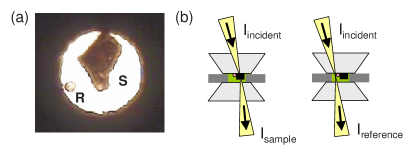
Pressure-dependent transmission measurements at room temperature were performed in the frequency range from 120 cm-1 to 20000 cm-1 using a Bruker IFS66v/S FTIR spectrometer combined with an infrared microscope (Bruker IRscope II). The pressure (up to 8 GPa) was generated by a diamond anvil cell (DAC) of Syassen-Holzapfel typeHuber et al. (1977) for the mid-infrared (MIR) to visible frequency range. The far-infrared (FIR) measurements were performed using a clamp diamond anvil cell (Diacell Cryo DAC Mega). The ruby luminescence method was used for the pressure determination Mao et al. (1986). The typical size of the piece of nanotube film used in one pressure experiment was approximately 100 100 for the MIR to visible frequency range and 250 250 for the FIR frequency range. Liquid argon served as pressure transmitting medium to ensure hydrostatic conditions. A typical loading of the DAC with a piece of carbon nanotube film is shown in Fig. 1(a). The piece of the nanotube film is seen in the transmission mode together with a small ruby ball used for the pressure determination. Fig. 1(b) illustrates the configuration of a transmission measurement through a DAC. The pressure-dependent transmission spectra were recorded by taking the ratio of intensity transmitted through the sample placed in the cell and the intensity of radiation transmitted through the argon (pressure transmitting medium), i.e., the transmittance is given as T=Isample/Ireference and the absorbance is calculated according to A=-log10T.
III Materials
The SWCNTs were prepared by the laser ablation technique using 1:1 Ni/Co catalyst, and thin films of the SWCNTs were obtained by vacuum filtration.Hennrich et al. (2002, 2003) The average diameter of the nanotubes is 1.2-1.4 nm. The average density of the nanotubes in the studied films were found to be 1.20.1 gcm-3.Hennrich et al. (2002) The purified nanotubes were obtained by treating them for 48h in HNO3 acid reflux.Hennrich et al. (2002) The purified and as-prepared nanotubes were then suspended in dimethyl-formamide (DMF) and sonicated before vacuum filtration.Hennrich et al. (2002) The purified thin films were finallyannealed to remove effects of acid treatment.
Due to the described treatment, we expect defects and shortenings for both purified and as-prepared SWCNTs .Dillon et al. (1999); Hu et al. (2003); Monthioux et al. (2001); Zhang et al. (2003) Thus, the adsorption of argon used here as pressure transmitting medium is expected to be important and needs to be considered. Adsorption of argon occurs at interstitial channels between the adjacent tubes, grooves and surface sites at the outer surface of the bundle, and the adsorption sites inside the empty nanotubes.Rols et al. (2005) As the studied nanotube films have not been subjected to the degassing procedure, it is not possible to estimate the amount of adsorbed argon, which is even otherwise a difficult task.
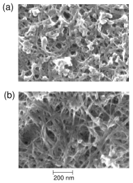
The scanning electron microscopy (SEM) images of the as-prepared and purified SWCNT films (Fig. 2) were recorded using a digital field emission scanning electron microscope (LEO 982) with magnification of 10x to 700000x. They illustrate the morphological differences between the two studied samples: The as-prepared film contains more (catalyst) impurities when compared to the purified film. From the SEM images, a rough estimation of the bundle diameters in both films could be made. The as-prepared and the purified films have bundle diameters in the range 6-25 nm and 12-40 nm, respectively. The larger bundle diameters observed in the SEM images of the purified film is similar to that observed by Martinez et al.Martinez et al. (2003) Both the as-prepared and the purified SWCNTs have small structural defects, with the purified film containing smaller amounts of non-carbonaceous impurities.
IV Results and Analysis
IV.1 Ambient conditions
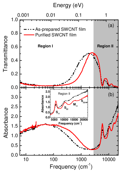
The transmittance and absorbance spectra of the as-prepared SWCNT film and purified SWCNT film are shown in Fig. 3. The spectra can be split into two main energy regions: Region I dominated by a strong FIR absorption band and Region II (shaded area) with several absorption bands labelled, S11, S22, M11, and S33/44 (see inset of Fig. 3), which correspond to interband transitions between the Van Hove singularities in the density of states. The S11, S22, and S33/44 bands in Region II denote interband transitions in semiconducting nanotubes, while the M11 band corresponds to interband transitions in metallic nanotubes. The subscripts denote the sequence of the involved Van Hove singularities with increasing energy. The absorption bands in Region II are sitting on top of a rather pronounced background. This background is related to an absorption band at around 5 eV due to the collective excitations of electrons in the graphene sheet.Kataura et al. (1999)
IV.1.1 Low-energy excitations
The low-energy spectra of the carbon nanotubes films are dominated by a pronounced absorption band centered in the FIR [see Region I in Fig. 3(b)]. For the analysis of the transmittance spectra in this low-energy range we applied two different models:
(i) Drude-Lorentz (DL) model, which describes the excitations of the itinerant charge carriers and the excitations of localized carriers and interband transitions: The dielectric function of a nanotube film according to the Drude-Lorentz model is given by
| (1) |
where is the complex dielectric function of the
nanotube film, is the core contribution to the
dielectric function, is the resonance frequency of the
excitation, and and are the plasma
frequency and damping of the excitation,
respectively.Dressel and Grner (2002) The plasma frequency is
defined by the expression where
is the number of charge carriers and is the free-electron mass.
The carbon nanotube film is considered as being dense enough to obtain
the optical conductivity spectrum by applying the simple DL model
to describe the transmittance spectrum of the carbon nanotube film
using the coherent transmission function.
(ii) Maxwell-Garnett effective medium approximation (called EMA model
in the following)
combined with the DL model for finite metallic particles embedded
in a dielectric medium:Cohen et al. (1973) Hereby, the nanotubes are
considered to be metallic wires of finite length embedded in a
dielectric host medium.Bommeli et al. (1997); Akima et al. (2006) The effective
dielectric function of the carbon nanotube film is given by the
expression
| (2) |
where is the dielectric function of the insulating dielectric host (air in our case) and is the dielectric function of carbon nanotubes in the film, described by the DL model [Eqn. (1)]. g is the geometrical factor which determines the shape of the particles embedded in the medium, and is equal to zero for an infinitely long needle. Therefore, in our case where the particles are nanotubes, g tends to zero but not exactly zero. v is the volume fraction of the nanotubes in the dielectric medium. According to the EMA model, the Drude peak related to the itinerant carriers is not centered at but at finite frequency. Within this picture, the peak position depends more on the geometrical factor of the material in the dielectric medium than on the carrier density.Tanner et al. (1975)
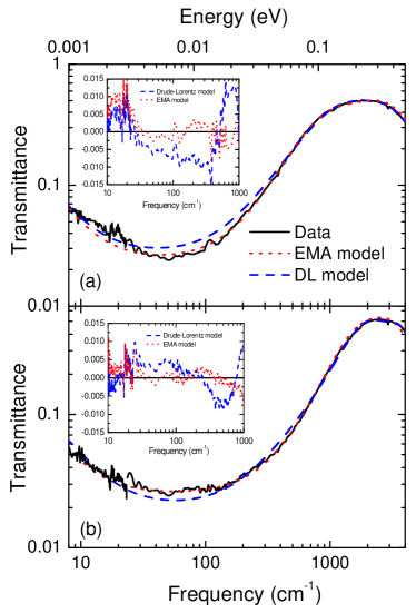
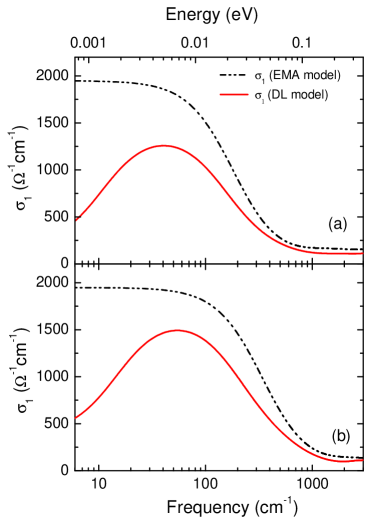
The fits of the transmittance spectra of both films using the two described models and the so-obtained optical conductivity spectra are shown in Figs. 4 and 5, respectively. Within the DL model, the FIR transmittance spectrum can be described by two components: a Drude contribution due to free-carriers in the metallic tubes and an absorption band described by a Lorentzian term centered below 100 cm-1. This gives rise to a maximum in the FIR optical conductivity, and most of the spectral weight lies in the band (see Fig. 5). Although a reasonable fit of the transmittance spectra could be obtained by using this simple DL model, the uncertainty in the fitting parameters of the Drude and the Lorentzian terms is large.
| Parameter | Film 1 | Film 2 |
|---|---|---|
| 1949 (cm-1) | 1949 (cm-1) | |
| 4639 cm-1 (139 THz) | 6345 cm-1 (190 THz) | |
| 184 cm-1 (5.52 THz) | 344 cm-1 (10.31 THz) |
Several experimental works which applied the DL model for the description of the optical response of SWCNTs attributed the non-metallic FIR contribution, i.e., the band centered around 100 cm-1, to excitations across the curvature-induced energy gap in metallic tubes.Ugawa et al. (1999); Itkis et al. (2002); Borondics et al. (2006); Kampfrath et al. (2008) However, as an alternative explanation for FIR peak the resonance due to finite size effects arising from the morphology of the film was proposed.Bommeli et al. (1997); Jeon et al. (2004); Akima et al. (2006) According to this interpretation, the EMA model should well describe the low-frequency optical conductivity in the SWCNT films. Indeed, the fit of the low-frequency optical response with the EMA model has the same quality as the fit with the DL model for both studied films (see insets Fig. 4). The best fit of the EMA model was obtained for the values g=0.00025 and v=0.7. The values of v, usually estimated based on the SEM images, lie in the expected range of 0.6-0.9 and the value of g is much smaller than 1, as expected for the nanotube bundles.Bommeli et al. (1997); Akima et al. (2006) Interestingly, it was sufficient to use only a Drude term to describe the low-energy optical response, consistent with earlier reports.Bommeli et al. (1997); Jeon et al. (2004); Akima et al. (2006) Accordingly, the optical conductivity obtained with the EMA model comprises a purely metallic contribution in the FIR frequency range (Fig. 5). Within the EMA approach the FIR contributions arise from itinerant charge carriers that may be localized along the tubes due to finite length effect, disorder and/or defects.
The parameters obtained from the fit of the EMA model are listed in Table. 1. For the as-prepared film we found a smaller plasma frequency and a smaller scattering rate compared to the purified SWCNT film. The smaller scattering rate might be due to the smaller extent of the defects in the sidewalls.
IV.1.2 Interband transitions
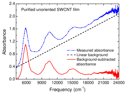
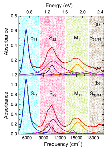
The energy of the interband transitions in the Region II was extracted in the following way: The background contribution in the MIR-to-visible part of the absorbance spectra due to - absorption was considered as being nearly linear within the measured energy range.Jost et al. (1999); Itkis et al. (2003) This linear background was subtracted from the measured spectra, in order to obtain only the contributions of the interband transitions. Fig. 6 illustrates the background subtraction procedure for one absorbance spectrum of the purified SWCNT film as an example. The background-subtracted spectra of both films were then fitted using Lorentz functions to obtain the energy of the interband transitions. Fig. 7 shows the background-subtracted absorbance spectra of the as-prepared and the purified films at ambient conditions together with the fitting curve and its components. The interband transition energies in both films obtained from the fittings are tabulated in Table 2. The results for the two films agree reasonably well. The fine structure observed in the absorbance spectra is due to the contributions of nanotubes with different diameters and chiralities.
| Label | Frequency (cm-1) | |
|---|---|---|
| Film 1 | Film 2 | |
| S11 (s) | 5843 | 5834 |
| S11 (w) | 7516 | 7516 |
| S22 (m) | 9771 | 9759 |
| S22 (m) | 10560 | 10500 |
| S22 (s) | 10764 | 10742 |
| M11 (w) | 13500 | 13438 |
| M11 (w) | 14372 | 14319 |
| M11 (s) | 15190 | 15235 |
| M11 (w) | 16834 | 16982 |
| S33/44 (w) | 18053 | 18053 |
| S33/44 (w) | 19157 | 19157 |
IV.2 Temperature dependence
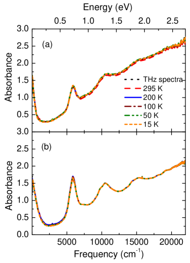
The temperature-dependent absorbance spectra of the as-prepared and the purified SWCNT film are depicted in Fig. 8. The spectra for both films are very similar and nearly temperature-independent over the entire measured frequency range (6-22000 cm-1). In earlier temperature-dependent infrared spectroscopic measurements on unoriented SWCNTs an extremely weak non-metallic temperature dependence was observed in the temperature range from 8 K to 298 K.Ugawa et al. (1999, 2001) A more recent temperature-dependent study on carbon nanotube networks by Borondics et al. also revealed only weak changes with respect to temperature in the FIR spectral regime.Borondics et al. (2006) This weak temperature dependence in the FIR absorption can be attributed to a tube-to-tube variation of the chemical potential.Kampfrath et al. (2008) Thus, our finding of the negligible temperature dependence of the studied as-prepared and purified SWCNT films, is in good agreement with earlier investigations.
IV.3 Pressure dependence
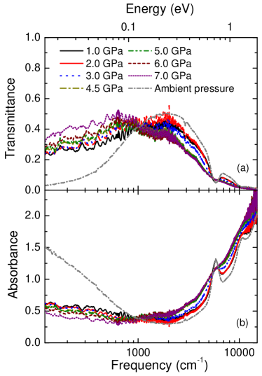
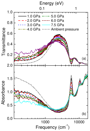
The as-prepared and the purified SWCNT films exhibit considerable changes in the electronic properties with the application of pressure in both the Regions I and II. Figs. 9 and 10 show the transmittance and absorbance spectra of the as-prepared and the purified unoriented SWCNT films for selected pressures up to 8 GPa in the FIR-to-visible frequency range. With increasing pressure, the interband transitions of the carbon nanotubes shift to lower frequencies and also exhibit a significant broadening. The intensity of the low-energy absorption (1000 cm-1) decreases with increasing pressure. In the following we will first present the pressure dependence of the low-energy excitations, and then focus on the interband transitions as a function of pressure.
IV.3.1 Low-energy excitations
The low-energy absorbance spectra of the carbon nanotubes were found to be significantly affected by the application of pressure (see Figs. 9 and 10). In Figs. 9 and 10 we also include the ambient-pressure spectra measured on the free-standing samples. The absorbance of the SWCNT films at the lowest measured pressure (1 GPa) is significantly lower compared to that at ambient pressure, with the effect being more drastic for the as-prepared SWCNT film. It seems that the adsorption of the pressure medium strongly influences the itinerant carriers.
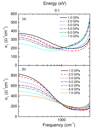
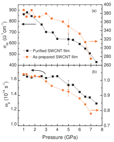
With increasing pressure the absorbance of the SWCNT films decreases continuously. For a quantitative analysis of the pressure-induced changes in the low-energy infrared response of the carbon nanotubes, the transmittance spectra were fitted with the EMA model as described in Section IV.1.1. The parameters of the EMA model, namely, the geometrical factor and the volume fraction, were assumed to be pressure-independent, in order to minimize the uncertainties in the analysis. This is also a reasonable assumption, since these parameters should not be changed with the application of external pressure. Similar to the ambient-pressure spectra, the low-frequency part of the spectra can be described by one Drude contribution. Fig. 11 shows the so-obtained optical conductivity spectra of the as-prepared and the purified SWCNT films for various pressures up to 7.5 GPa. The low-frequency optical conductivity decreases with increasing pressure, in good qualitative agreement with the absorbance spectra. The dc conductivity and the plasma frequency of the Drude term obtained from the fitting decrease with increasing pressure (see Fig. 12). The pressure dependence of both films are in qualitative agreement.
IV.3.2 Interband transitions
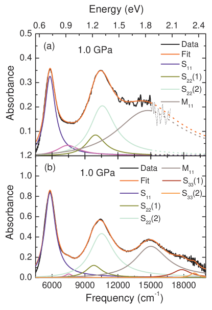
For a quantitative analysis of the pressure-induced changes in the interband transitions their energies were extracted from the absorbance spectra for all measured pressures using the same procedure as for the absorbance spectra at ambient conditions (i.e., background subtraction and fitting with Lorentzian functions, see Section IV.1.2). For an illustration of the procedure we show in Fig. 13 the background-subtracted absorbance spectra of the as-prepared and the purified SWCNT films for the lowest measured pressure, together with the fitting curve and its components. It is obvious that the fine structure in the optical absorption bands observed in the spectrum at ambient pressure (see Fig. 7) is obscured even at low pressures by pressure-induced broadening effects. For the same reason, only the strong and most obvious transitions have been considered for the fitting using Lorentzian functions, and excellent fits were accomplished.
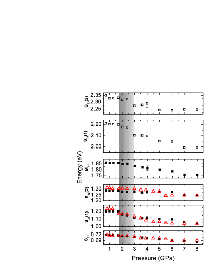
The so-obtained energies of the interband transitions with the strongest contribution (labeled in Fig. 13) of both SWCNT films are shown in Fig. 14 as a function of pressure. In case of the as-prepared SWCNT film only the first two interband transitions could be unambiguously traced as a function of pressure due to the low signal-to-noise ratio above 15000 cm-1. The pressure dependence of the interband transitions in both SWCNT films are in good agreement and the important observations are as follows: (i) All interband transitions exhibit a small redshift with increasing pressure up to the critical pressure 2.0 GPa. (ii) Above the redshift of the interband transitions is enhanced. This results in an (iii) anomaly in the pressure-induced shift at .
V Discussion
V.1 Low-energy excitations
The FIR conductivity of the SWCNT films is nearly independent of temperature. The complex dielectric constant measurements by Hilt et al.,Hilt et al. (2000) indicate that the transport properties of the SWCNT mats can be well described by a Drude model with a negligible temperature dependence. They observed that the conductivity at very low frequencies (around 285 GHz) is dominated by localized carriers. Based on temperature-dependent measurements on unoriented carbon nanotubes, including nanotubes embedded in the polymer matrix, is was concluded that there is a localization of carriers in the bundles and along the tubes.Hilt et al. (2000); Benoit et al. (2002); Fuhrer et al. (1999) Additionally, theoretical studies found that the localization of carriers plays a major role in determining the low-energy properties of carbon nanotubes.Jiang et al. (2001); Hjort and Stafstrm (2001) Hence, carrier localization effects should be considered in the discussion of our results.
The application of pressure strongly influences the Drude conductivity of the as-prepared and the purified SWCNT films: The dc optical conductivity and the plasma frequency decrease with increasing pressure (see Fig. 12). Hence, pressure enhances the localization effects of the charge carriers. Recent theoretical investigations on the localization effects on deformed nanotubes indeed suggest that with increasing deformations, the localization length of the carriers decreases leading to a decrease in the conductivity.Bu et al. (2002); Hjort and Stafstrm (2001) In addition to the localization effects, the electronic band structure of the nanotubes is expected to change considerably under pressure due to structural changes in the nanotubes. The deformation of the nanotubes induces symmetry breaking and - hybridization effects due to the mixing of states in the polygonized nanotubes. A possible interaction between the facing layers in the radially-deformed nanotubes further modifies the low-energy electronic structure strongly.Park et al. (1999); Yang and Han (2000); Lammert et al. (2000) These changes eventually lead to the opening or closing of the gap at the Fermi level and thereby causing a metal-to-semiconductor transition or vice-versa in metallic tubes or small-gap nanotubes, respectively.Charlier et al. (1996); Park et al. (1999); Mazzoni and Chacham (2000); Lammert et al. (2000); Guelseren et al. (2002); Lu et al. (2003) Although this could lead to competing effects on the low-energy conductivity of SWCNT films, we observe an overall decrease in the optical conductivity with increasing pressure. It seems that only a small fraction of the small-gap nanotubes in our sample undergo a semiconductor-to-metal transition under pressure.
Therefore, we tentatively assign the pressure-induced decrease in the low-energy conductivity to the increasing localization of carriers caused by defects and deformations combined with the decrease in the density of states close to the Fermi level due to the radial deformation of the SWCNTs. This interesting observation calls for further experimental investigations of the pressure-dependent electronic properties of carbon nanotubes down to lower frequencies. It is important to note that the Drude parameters (dc conductivity, plasma frequency, see Fig. 12) obtained from the analysis of our data have relatively large error bars, since it is not possible to study the frequency range below 100 cm-1 with our technique due to the diffraction limit. This could explain why we do not find an anomaly in the pressure dependence of these parameters at .
V.2 Interband transitions
Pressure and temperature affect the interband transitions of the carbon nanotubes in a very different way. Although the electronic properties of both the as-prepared and the purified films show considerable changes with the application of pressure, the two SWCNT films exhibit temperature-independent properties. The temperature-dependent energy shifts of the interband transitions of the carbon nanotubes in Region II, are expected to be either positive or negative depending on the chiral angle in the photoluminescence measurement.Li et al. (2004) Recent theoretical studies found that the temperature-dependence of the bandgap of the carbon nanotubes is relatively small compared to the bulk semiconductors, and the maximum temperature-induced shift was calculated to be around 10 meV.Capaz et al. (2005) In addition to the small temperature-induced changes which are highly chirality-dependent, it was suggested that the temperature-dependence of optical transition energies of the nanotubes in the bundles are dominated by the thermal expansion of the nanotubes’ environment.Cronin et al. (2006) Very recent experimental and theoretical temperature-dependent studies on semiconducting nanotubes suggest that the positive or negative energy shifts could be attributed to external strain, while the broadening of the transitions might be attributed to electron-phonon interactions.Karaiskaj and Mascarenhas (2007) These effects are not relevant here, since the nanotube films studied within this work are free-standing films. The interband transitions of the unoriented and unsegregated nanotube films are generally convolutions of the transitions corresponding to tubes with different diameters and chiralities. These transitions are therefore quite broad when compared to the small changes expected during the change in temperature. Thus, the observation of an “averaged-out” temperature change in the nanotube films which give rise to the temperature-independent NIR-visible frequency absorbance spectra is plausible.
The changes in the optical transition energies under hydrostatic pressure were theoretically investigated in Refs. Capaz et al. (2004); Liu et al. (2008) A “family behavior” in the pressure coefficients, i.e., having positive or negative values of pressure coefficients depending on chirality, was found for semiconducting SWCNTs. A similar behavior was reported for the changes of the band gap under uniaxial stress.Yang et al. (1999); Yang and Han (2000); Gartstein et al. (2003) On the contrary, experimentally an overall shift of the interband transitions to lower energies with increasing pressure was observed in both bundled and individualized nanotubes.Kazaoui et al. (2000); Wu et al. (2004); Deacon et al. (2006) The shift of the interband transitions to lower energies was attributed to the intertube interactions and/or symmetry breaking in the very early high-pressure optical absorption measurements.Kazaoui et al. (2000) Photoluminescence measurements on individualized nanotubes in aqueous solution of surfactant demonstrated that the negative pressure coefficient is an intrinsic property of the individual nanotubes and the intertube interactions do not play a role.Wu et al. (2004) Furthermore, - hybridization was suggested as an explanation for the overall negative pressure coefficient, at least in the low-pressure regime (below 1.3 GPa).Wu et al. (2004)
In an alternative approach, Deacon et al. attributed the downshift of the interband transitions to the interaction of the nanotubes with the surrounding surfactant:Deacon et al. (2006) The dielectric constant of the surfactant solution (which is the surrounding medium) increases with increasing pressure, causing a reduction of the Coulomb interactions. Also a recent investigation on individual double-walled nanotubes under pressure showed that the interaction of nanotubes with the surrounding medium is very important.Puech et al. (2006) The pressure coefficients of the Raman bands were highly dependent on the employed pressure transmitting medium.Puech et al. (2006) However, the lowering of the energy of the interband transitions was also observed in the case of a solid pressure transmitting medium, for which adsorption of the pressure transmitting medium can be ruled out.Kazaoui et al. (2000); Kuntscher et al. (2008) Therefore, the decrease in energy of the interband transitions with increasing pressure cannot be solely attributed to the effect of the surrounding medium, and thus hybridization effects have to be considered.
The - hybridization not only plays a significant role in the electronic band-structure of the small diameter tubes Blase et al. (1994) but also in polygonized and deformed tubes. The changes in the electronic properties of the SWCNTs with polygonized cross-sections were theoretically investigated.Charlier et al. (1996); Liu et al. (2008) According to these studies, the radial deformation of the nanotubes strongly influences the band-structure and hence the optical properties of the nanotubes. It was found that the deformation-induced hybridization effects and symmetry-breaking lower the conduction-band states towards the Fermi level,Charlier et al. (1996); Liu et al. (2008) which nicely explains the redshift of the interband transitions observed in our pressure-dependent optical data.
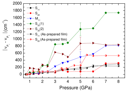
The pressure-induced shift of the interband transitions with respect to the lowest applied pressure is depicted in Fig. 15. The results for both films are very similar. Compared to the lowest-energy transition S11, the transitions in semiconducting tubes at higher energies, namely S22 and S33, and those in metallic tubes, M11, are more sensitive regarding pressure above 2 GPa compared to the first transition S11. According to earlier pressure-dependent optical absorption studies Kazaoui et al. (2000) the interband transitions of semiconducting tubes vanish at a pressure of 4.1 GPa, while the transitions corresponding to the metallic tubes persist. In contrast, we observe that the pressure dependence of the interband transitions in semiconducting and metallic tubes are very similar, with comparable pressure coefficients (see Fig. 15). The overall red-shift of the interband transitions is in qualitative agreement with earlier pressure-dependent studies on SWCNTs.Kazaoui et al. (2000); Wu et al. (2004) However, we observe much smaller energy shifts than those in earlier reports.Kazaoui et al. (2000) For example, the shift of the energy of S11 transition in the measurements by Kazaoui et al. at 4 GPa is nearly twice as much as that found in our data. This discrepancy is probably due to the less hydrostatic conditions present during previous experiments. In our experiment we used a more hydrostatic pressure medium (argon), which minimizes strains due to non-hydrostaticity, thus reducing the extent of the red-shift and the broadening of the observed absorption bands.
On applying pressure, the interband transitions show small shifts up to 2 GPa. Above this critical pressure, the energy of the interband transitions decrease more drastically with increasing pressure, causing an anomaly in the pressure dependence at . Several Raman spectroscopic investigations also reported the disappearance or loss of intensity of the radial breathing mode (RBM) of nanotubes and anomalies in the tangential mode of nanotubes at pressures in the range 1.5-2 GPa, which were attributed to the radial deformation of nanotubes.Loa (2003)
There is an enormous number of theoretical studies addressing the pressure-induced structural deformations in carbon nanotubes. The circular cross-section of the nanotubes undergoes significant deformation under pressure.Okada et al. (2001); S.Reich et al. (2002); Chan et al. (2003) It was suggested that the circular cross-section of nanotubes deforms and stabilizes at an oval, elliptical, racetrack-like or peanut-shaped cross-section.S.Reich et al. (2002); Chan et al. (2003); Sluiter and Kawazoe (2004); Li and Chou (2004); Zhang et al. (2004); Elliott et al. (2004); Capaz et al. (2004) The nature of the phase transition and the deformation in the carbon nanotubes are very complex with the existence of metastable states, and are highly dependent on the nanotube diameter just like the other properties of nanotubes.Sluiter and Kawazoe (2004); Elliott et al. (2004); Hasegawa and Nishidate (2006) Despite some discrepancies concerning the details of the high-pressure phase of the carbon nanotubes, it is well established through both experimental and theoretical studies that the discontinuous radial deformation in SWCNTs occurs at a certain critical pressure Pc. The value of Pc decreases with increasing carbon nanotube diameter and follows the relation Pc 1/d3 for both individual SWCNTsCapaz et al. (2004); Zhang et al. (2004); Li and Chou (2004); Hasegawa and Nishidate (2006) and bundled SWCNTs.Zhang et al. (2004); Elliott et al. (2004); Li and Chou (2004); Capaz et al. (2004) For nanotubes grown by the laser ablation technique, with an average diameter of 1.2-1.4 nm, the critical transition pressure is expected to be about 2 GPa.Chan et al. (2003); Sluiter and Kawazoe (2004); Elliott et al. (2004); Capaz et al. (2004); Hasegawa and Nishidate (2006) Hence, our experimental finding of an anomaly at Pc 2 GPa is in agreement with the above-mentioned earlier reports. Furthermore, a recent theoretical investigation on the nature of the deformation of the SWCNTs found that the SWCNTs of diameter less than 2.5 nm undergo a transition from a circular to an oval shape and do not collapse, while the tubes with larger diameters do collapse.Hasegawa and Nishidate (2006) Hence, the anomaly found in our experiments could be attributed to the structural phase transition in the nanotubes, where the circular cross-section is deformed to an oval shape.
Resonant Raman studies on individualized nanotubes under pressure report the critical pressures 10 GPa and 4 GPa for radial deformation for nanotubes of diameters 0.8-0.9 nm and 1.2-1.3 nm, respectively.Lebedkin et al. (2006) Furthermore, it is interesting to note that some experiments found no significant deformation effects up to high pressures in bundled nanotubes.Amer et al. (2004); Merlen et al. (2005, 2006); Monteverde and Nnez-Regueiro (2005) For example, no anomaly was observed by resonant Raman spectroscopy on carbon nanotubes for pressures up to 40 GPa.Merlen et al. (2005) The absence of an anomaly was attributed to the adsorption of argon in the tubes.Merlen et al. (2005) Other recent measurements on purified nanotubes also suggest that the pressure transmitting medium plays a decisive role for the critical pressure of the the structural phase transition, due to adsorption effects.Amer et al. (2004); Proctor et al. (2006) In contrast to these reports, we do observe an anomaly in the pressure dependence of the optical transitions when using argon as pressure transmitting medium. Our observation of an anomaly does, however, not exclude the physical adsorption of argon on the SWCNTs during our pressure measurements.
Although the electronic properties of bundled carbon nanotubes are changed considerably with increasing pressure, the pressure-induced changes are almost completely reversible: The position of the interband transitions were reversible on releasing pressure, but the intensities of the interband transitions were not regained completely. The reversibility of the pressure-induced transformations in the nanotubes has been controversial.Loa (2003); Sluiter and Kawazoe (2004) Sluiter et al., suggested a phase diagram for SWCNT bundles which could explain the inconsistency in the reversibility of the pressure-induced changes in various experimental investigations.Sluiter and Kawazoe (2004) According to this phase diagram, the critical pressure at which the radial deformation occurs is lower than the cross-linking pressure. At the cross-linking pressure, the deformed nanotubes in the bundles start linking to each other similar to a polymerization effect. Therefore, the reversibility of the experimental data may not be observed when the highest measured pressure is above the cross-linking pressure. Despite the observed reversibility of the pressure-induced effects in our data, the crosslinking of the nanotubes cannot be completely ruled out in our experiments: Density functional electronic structure simulations predict that the cross-linking is reversible when the circumference of the nanotubes is greater than 3.8 nm.Sluiter and Kawazoe (2004) The SWCNTs in our work have an average circumference of 4.1 nm, which implies that the cross-linking, if it occurs, would be completely reversible upon pressure release.
VI Conclusions
We have investigated the optical properties of as-prepared and purified unoriented SWCNT films over a broad frequency range (FIR-to-visible) as a function of temperature and pressure (up to 8 GPa). Both the as-prepared and the purified SWCNT film exhibit nearly temperature-independent properties. With increasing pressure the low-energy absorbance monotonically decreases due to enhanced carrier localization. The energy of the interband transitions decreases with application of pressure due to the significant hybridization and symmetry-breaking effects. At around 2 GPa the shifts of the interband transitions show an anomaly, which can be attributed to a pressure-induced structural phase transition.
Acknowledgements.
We thank A. Abouelsayed and M. Kappes for fruitful discussions. We acknowledge the ANKA Angströmquelle Karlsruhe for the provision of beamtime and thank B. Gasharova, Y.-L. Mathis, D. Moss, and M. Süpfle for assistance at the beamline ANKA-IR. We thank M. Dressel for the opportunity to perform THz frequency range measurements at the University Stuttgart, 1. Physikalisches Institut, and F. Rauscher and K. Venkataramani for their help during the THz measurements. We also thank D. Trojak for her support regarding the SEM images of the studied nanotube films. Financial support by the Deutsche Forschungsgemeinschaft (KU 1432/3-1) and the Hungarian Academy of Sciences (grant No. DFG/183) is gratefully acknowledged.References
- Dresselhaus et al. (1996) M. Dresselhaus, G. Dresselhaus, and P. Eklund, Science of fullerenes and carbon nanotubes (Academic press, San Diego, 1996).
- Reich et al. (2004) S. Reich, C. Thomsen, and J. Maultzsch, Carbon nanotubes: Basic concepts and physical properties (Wiley-VCH, Weinheim, 2004).
- Lefebvre et al. (2004) J. Lefebvre, P. Finnie, and Y. Homma, Phys. Rev. B 70, 045419 (2004).
- Capaz et al. (2005) R. B. Capaz, C. D. Spataru, P. Tangney, M. L. Cohen, and S. G. Louie, Phys. Rev. Lett. 94, 036801 (2005).
- Cronin et al. (2006) S. B. Cronin, Y. Yin, A. Walsh, R. B. Capaz, A. Stolyarov, P. Tangney, M. L. Cohen, S. G. Louie, A. K. Swan, M. S. ’́Unl’́u, et al., Phys. Rev. Lett. 96, 127403 (2006).
- Ugawa et al. (1999) A. Ugawa, A. G. Rinzler, and D. B. Tanner, Phys. Rev. B 60, R11305 (1999).
- Ugawa et al. (2001) A. Ugawa, J. Hwang, H. H. Gommans, H. Tashiro, A. G. Rinzler, and D. B. Tanner, Current Appl. Phys. 1, 45 (2001).
- Hilt et al. (2000) O. Hilt, H. B. Brom, and M. Ahlskog, Phys. Rev. B 61, R5129 (2000).
- Hone et al. (1998) J. Hone, I. Ellwood, M. Muno, A. Mizel, M. L. Cohen, and A. Zettl, Phys. Rev. Lett. 80, 1042 (1998).
- Borondics et al. (2006) F. Borondics, K. Kamarás, M. Nikolou, D. B. Tanner, Z. H. Chen, and A. G. Rinzler, Phys. Rev. B 74, 045431 (2006).
- Benoit et al. (2002) J. Benoit, B. Corraze, and O. Chauvet, Phys. Rev. B 65, 241405 (2002).
- Fuhrer et al. (1999) M. Fuhrer, M. Cohen, A. Zettl, and V. Crespi, Solid State Commun. 109, 105 (1999).
- Jiang et al. (2001) J. Jiang, J. Dong, H. T. Yang, and D. Y. Xing, Phys. Rev. B 64, 045409 (2001).
- Loa (2003) I. Loa, J. Raman. Spectrosc 34, 611 (2003), and references therein.
- Lebedkin et al. (2006) S. Lebedkin, K. Arnold, O. Kiowski, F. Hennrich, and M. Kappes, Phys. Rev. B 73, 094109 (2006), and references therein.
- Tang et al. (2000) J. Tang, L.-C. Qin, T. Sasaki, M. Yudasaka, A. Matsushita, and S. Iijima, Phys. Rev. Lett. 85, 1887 (2000).
- Sharma et al. (2001) S. Sharma, S. Karmakar, S. Sikka, P. Teredesai, A. Sood, A. Govindaraj, and C. Rao, Phys. Rev. B 63, 205417 (2001).
- Rols et al. (2001) S. Rols, I. Goncharenko, R. Almairac, J. Sauvajol, and I. Mirebeau, Phys. Rev. B 64, 153401 (2001).
- Bommeli et al. (1997) F. Bommeli, L. Degiorgi, P. Wachter, W. S. Bacsa, W. A. de Heer, and L. Forro, Synthetic Metals 86, 2307 (1997).
- Itkis et al. (2002) M. E. Itkis, S. Niyogi, M. E. Meng, M. A. Hamon, H. Hu, and R. C. Haddon, Nano Letters 2, 155 (2002).
- Itkis et al. (2003) M. E. Itkis, D. E. Perea, S. Niyogi, S. M. Richard, M. A. Hamon, H. Hu, B. Zhao, and R. C. Haddon, Nano Letters 3, 309 (2003).
- Kazaoui et al. (2000) S. Kazaoui, N. Minami, H. Yamawaki, K. Aoki, H. Kataura, and Y. Achiba, Phys. Rev. B 62, 1643 (2000).
- Wu et al. (2004) J. Wu, W. Walukiewicz, W. Shan, E. Bourret-Courchesne, J. A. III, K. Yu, E. Haller, K. Kissell, S. Bachilo, R. B. Weisman, et al., Phys. Rev. Lett. 93, 017404 (2004).
- Huber et al. (1977) G. Huber, K. Syassen, and W. B. Holzapfel, Phys. Rev. B 15, 5123 (1977).
- Mao et al. (1986) H. K. Mao, J. Xu, and P. M. Bell, J. Geophys. Res [Atmos.] 91, 4673 (1986).
- Hennrich et al. (2002) F. Hennrich, S. Lebedkin, S. Malik, J. Tracey, M. Barczewski, H. Roesner, and M. Kappes, Phys. Chem. Chem. Phys. 4, 2273 (2002).
- Hennrich et al. (2003) F. Hennrich, R. Wellmann, S. Malik, S. Lebedkin, and M. Kappes, Phys. Chem. Chem. Phys. 5, 178 (2003).
- Dillon et al. (1999) A. Dillon, T. Gennett, K. Jones, J. Alleman, P. Parilla, and M. Heben, Adv. Mater. 11, 1354 (1999).
- Hu et al. (2003) H. Hu, B. Zhao, M. Itkis, and R. Haddon, J. Phys. Chem. B 107, 13838 (2003).
- Monthioux et al. (2001) M. Monthioux, B. Smith, B. Burteaux, A. Claye, J. Fischer, and D. Luzzi, Carbon 39, 1251 (2001).
- Zhang et al. (2003) J. Zhang, H. Zou, Q. Qing, Y. Yang, Q. Li, Z. Liu, X. Guo, and Z. Du, J. Phys. Chem. B 107, 3712 (2003).
- Rols et al. (2005) S. Rols, M. Johnson, P. Zeppenfeld, M. Bienfait, O. Vilches, and J. Schneble, Phys. Rev. B 71, 155411 (2005).
- Martinez et al. (2003) M. Martinez, M. Callejas, A. Benito, M. Cochet, T. Seeger, A. Ansón, J. Schreiber, C. Gordon, C. Marhic, O. Chauvet, et al., Nanotechnology 14, 691 (2003).
- Kataura et al. (1999) H. Kataura, Y. Kumazawa, Y. Maniwa, I. Umezu, S. Suzuki, Y. Ohtsuka, and Y. Achiba, Synthetic Metals 103, 2555 (1999).
- Dressel and Grner (2002) M. Dressel and G. Grner, Electrodynamics of Solids (Cambridge University press, UK, 2002).
- Cohen et al. (1973) R. Cohen, G. Cody, M. Coutts, and B. Abeles, Phys. Rev. B 8, 3689 (1973).
- Akima et al. (2006) N. Akima, Y. Iwasa, S. Brown, A. M. Barbour, J. Cao, J. L. Musfeldt, H. Matsui, N. Toyota, M. Shiraishi, H. Shimoda, et al., Adv. Mater. 18, 1166 (2006).
- Tanner et al. (1975) D. B. Tanner, A. J. Sievers, and R. A. Buhrman, Phys. Rev. B 11, 1330 (1975).
- Kampfrath et al. (2008) T. Kampfrath, K. von Volkmann, C. M. Aguirre, P. Desjardins, R. Martel, M. Krenz, C. Frischkorn, M. Wolf, and L. Perfetti, Phys. Rev. Lett. 101, 267403 (2008).
- Jeon et al. (2004) T.-I. Jeon, K.-J. Kim, C. Kang, I. Maeng, J.-H. Son, K. An, J. Lee, and Y. Lee, J. Appl. Phys. 95, 5736 (2004).
- Jost et al. (1999) O. Jost, A. A. Gorbunov, W. Pompe, T. Pichler, R. Friedlein, M. Knupfer, M. Reibold, H.-D. Bauer, L. Dunsch, M. S. Golden, et al., Appl. Phys. Lett. 75, 2217 (1999).
- Hjort and Stafstrm (2001) M. Hjort and S. Stafstrm, Phys. Rev. B 63, 113406 (2001).
- Bu et al. (2002) W. Bu, J. Jiang, and J. Dong, Phys. Lett. A 302, 125 (2002).
- Park et al. (1999) C.-J. Park, Y.-H. Kim, and K. Chang, Phys. Rev. B 60, 10656 (1999).
- Yang and Han (2000) L. Yang and J. Han, Phys. Rev. Lett. 85, 154 (2000).
- Lammert et al. (2000) P. Lammert, P. Zhang, and V. Crespi, Phys. Rev. Lett. 84, 2453 (2000).
- Charlier et al. (1996) J.-C. Charlier, P. Lambin, and T. Ebbesen, Phys. Rev. B 54, R8377 (1996).
- Mazzoni and Chacham (2000) M. Mazzoni and H. Chacham, Appl. Phys. Lett. 76, 1561 (2000).
- Guelseren et al. (2002) O. Guelseren, T. Yildirim, S. Ciraci, and C. Kilic, Phys. Rev. B 65, 155410 (2002).
- Lu et al. (2003) J.-Q. Lu, J. Wu, W. Duan, F. Liu, B.-F. Zhu, and B.-L. Gu, Phys. Rev. Lett. 90, 156601 (2003).
- Li et al. (2004) L. J. Li, R. J. Nicholas, R. S. Deacon, and P. A. Shields, Phys. Rev. Lett. 93, 156104 (2004).
- Karaiskaj and Mascarenhas (2007) D. Karaiskaj and A. Mascarenhas, Phys. Rev. B 75, 115426 (2007).
- Capaz et al. (2004) R. Capaz, C. Spataru, P. Tangney, M. Cohen, and S. Louie, phys. stat. sol. (b) 241, 3352 (2004).
- Liu et al. (2008) G. Liu, X. Wang, J. Chen, and H. Lu, phys. stat. sol. (b) 245, 689 (2008).
- Yang et al. (1999) L. Yang, M. Anantram, J. Han, and J. Lu, Phys. Rev. B 60, 13874 (1999).
- Gartstein et al. (2003) Y. Gartstein, A. Zakhidov, and R. Baughman, Phys. Rev. B 68, 115415 (2003).
- Deacon et al. (2006) R. Deacon, K.-C. Chuang, J. Doig, I. Mortimer, and R. Nicolas, Phys. Rev. B 74, 201402(R) (2006).
- Puech et al. (2006) P. Puech, E. Flahaut, A. Sapelkin, H. Hubel, D. Dunstan, G. Landa, and W. Bacsa, Phys. Rev. B 73, 233408 (2006).
- Kuntscher et al. (2008) C. A. Kuntscher, K. Thirunavukkuarasu, K. Kamarás, F. Simon, and D. A. Walters, phys. stat. sol. (b) 245, 2288 (2008).
- Blase et al. (1994) X. Blase, L. Benedict, E. Shirley, and S. Louie, Phys. Rev. Lett. 72, 1878 (1994).
- Okada et al. (2001) S. Okada, A. Oshiyama, and S. Saito, J. Phys. Soc. Jpn 70, 2345 (2001).
- S.Reich et al. (2002) S.Reich, C. Thomsen, and P. Ordejon, Phys. Rev. B 65, 153407 (2002).
- Chan et al. (2003) S.-P. Chan, W.-L. Yim, X. Gong, and Z.-F. Liu, Phys. Rev. B 68, 075404 (2003).
- Sluiter and Kawazoe (2004) M. Sluiter and Y. Kawazoe, Phys. Rev. B 69, 224111 (2004).
- Li and Chou (2004) C. Li and T.-W. Chou, Phys. Rev. B 69, 073401 (2004).
- Zhang et al. (2004) X. Zhang, D. Sun, Z. Liu, and X. Gong, Phys. Rev. B 70, 035422 (2004).
- Elliott et al. (2004) J. Elliott, J. Sandler, A. Windle, R. Young, and M. Shaffer, Phys. Rev. Lett. 92, 095501 (2004).
- Hasegawa and Nishidate (2006) M. Hasegawa and K. Nishidate, Phys. Rev. B 74, 115401 (2006).
- Amer et al. (2004) M. Amer, M. El-Ashry, and J. Maguire, J. Chem. Phys. 292, 702 (2004).
- Merlen et al. (2005) A. Merlen, N. Bendiab, P. Toulemonde, A. Aouizerat, A. S. Miguel, J. Sauvajol, G. Montagnac, H. Cardon, and P. Petit, Phys. Rev. B 72, 035409 (2005).
- Merlen et al. (2006) A. Merlen, P. Toulemonde, N. Bendiab, A. Aouizerat, J. Sauvajol, G. Montagnac, H. Cardon, P. Petit, and A. S. Miguel, phys. stat. sol. (b) 243, 690 (2006).
- Monteverde and Nnez-Regueiro (2005) M. Monteverde and M. Nnez-Regueiro, Phys. Rev. Lett. 94, 235501 (2005).
- Proctor et al. (2006) J. Proctor, M. Halsall, A. Ghandour, and D. Dunstan, J. Phys. Chem. Solids 67, 2468 (2006).