Modeling electrolytically top gated graphene
Abstract
We investigate doping of a single-layer graphene in the presence of electrolytic top gating. The interfacial phenomena is modeled using a modified Poisson-Boltzmann equation for an aqueous solution of simple salt. We demonstrate both the sensitivity of graphene’s doping levels to the salt concentration and the importance of quantum capacitance that arises due to the smallness of the Debye screening length in the electrolyte.
pacs:
52.40.Hf, 52.25.Vy, 52.35.FpI Introduction
Carbon nano-structures show great promise in many applications, including chemical and biological sensors. While carbon nanotubes (CNTs) have been extensively studied in that context for quite some time Kong_2000 ; Kauffman_2008 , investigations of graphene as a sensor are only beginning to appear Schedin_2007 ; Robinson_2008 ; Ang_2008 . Sensory function of carbon nano-structures is generally implemented in the configuration of a field effect transistor (FET), with a prominent role played by the gate potential that controls the current through the device. Biochemical applications require good understanding of the interaction of carbon nano-structures with aqueous solutions Ang_2008 , often in the context of the electrochemical top gating Das_2008 . While significant progress has been achieved in understanding the interaction of CNT-FETs with the electrolytic environment Kruger_2001 ; Rosenblut_2002 ; Heller_2006 , similar studies involving graphene have appeared only very recently Das_2008 , focusing on the screening effect of an ion solution on charge transport through graphene based FETs Chen_2009 , as well as on the measurement of the quantum capacitance of graphene as an ultimately thin electrode in an aqueous solution Xia_2009 .
The top gating of a graphene based FET with a solid or liquid electrolyte presents several advantages compared to the conventional back gating with a metallic electrode. Upon application of gate voltage, free ions in the electrolyte re-distribute themselves, forming an electrostatic double layer (EDL) at the interface between graphene and the electrolytic solution Castro_2009 . Depending on the ion concentration, the EDL can be only a few nanometers thick, while still providing efficient shielding of graphene. As a consequence, the capacitance of the EDL in an electrolyte can be much higher than the capacitance of the back gate, which is typically separated from graphene with a layer of SiO2 a few hundred nanometers thick Castro_2009 . This property of the EDL enables a much better control of the surface potential on the graphene layer, while requiring a much lower operating voltage that needs to be applied to the reference electrode in the electrolyte than voltages currently used with back gates Castro_2009 . The applied voltage then modifies the chemical potential of graphene, resulting in changes in its observable properties such as conductance. Since properties of the EDL depend on the ion concentration, monitoring the resulting changes in graphene’s conductance can provide a means for sensor application, e.g., in measuring the amount of salt in the solution.
On the other hand, referring to the electrical model of the electrolytic gating as a series connection of capacitors Bard_2001 , the high gate capacitance in the electrolyte gives a much more prominent role to the quantum capacitance of graphene than does the back gate Xia_2009 ; Fang_2007 ; Guo_2007 ; Giannazzo_2009 . In addition, doping levels of an electrolytically top gated graphene have been reported recently Das_2008 to be much higher than those obtained with the conventional back gate Sonde_2009 . At the same time, mobile ions in the solution seem to provide a much more effective screening of charged impurities underneath the graphene, thereby significantly increasing the charge carrier mobility in graphene in comparison to some other high- dielectric environments Ponomarenko_2009 . All these facts indicate that electrolytic top gating provides a means to develop high performance FETs.
While the above few experimental observations reveal quite fascinating aspects of the graphene-electrolyte interaction, theoretical modeling of this system seems to be lagging behind the experiment. It is therefore desirable, and tempting to discuss doping of a single layer of graphene by a remote gate electrode immersed in a thick layer of electrolyte by using two simple models: one describing graphene’s electron band structure in the linear energy dispersion approximation Castro_2009 , and the other describing the distribution of ions in the electrolyte by a one-dimensional (1D) Poisson-Boltzmann (PB) model, which takes advantage of the planar symmetry of the problem Bard_2001 . However, it should be emphasized that the experiments involving electrolytic top-gating of both carbon nanotubes Kruger_2001 ; Rosenblut_2002 and graphene Das_2008 ; Chen_2009 use rather hight voltages, on the order of 1-2 V, which can cause significant crowding of counter-ions at the electrolyte-graphene interface. It is therefore necessary to go beyond the standard PB model by taking into account the steric effects, i.e., the effects of finite size of ions in the solution. To that aim, we shall use the modified PB (mPB) model developed by Borukhov et al.Borukhov_1997 ; Kilic_2007 , which retains analytical tractability of the original 1D-PB model. In addition, applied voltages beyond 1 V also require taking into account non-linearity of graphene’s band energy dispersion, giving small but noticeable corrections to the linear approximation.
We shall consider here a simple 1:1 electrolyte representing an aqueous solution of NaF because both the Na+ and F- ions are chemically inert allowing us to neglect their specific adsorption on the graphene surface Chen_2009 ; Bard_2001 . In particular, we shall analyze the density of doped charge carriers in graphene at room temperature (RT) as a function of both the applied voltage and the salt concentration to elucidate graphene’s sensor ability. In addition, we shall evaluate the contributions of both graphene and the EDL in the total gate capacitance in terms of the applied voltage to reveal the significance of quantum capacitance, as well as to elucidate the behavior of the EDL under high voltages. We shall cover broad ranges of both the salt concentration, going from M to a physiologically relevant value, and the applied voltage, going up to about 2 V.
After outlining in section II our theoretical models for graphene and the EDL layer, we shall introduce several reduced quantities of relevance for these two vastly different systems and present our results in section III. Concluding remarks are given in section IV. Note that we shall use gaussian units () throughout the paper, unless otherwise explicitly stated.
II Theoretical model
Graphene is a semi-metal, or a zero-gap semiconductor because its conducting and valence electron bands touch each other only at two isolated points in its two-dimensional (2D) Brillouin zone Castro_2009 . The conical shape of these bands in the vicinity of these points gives rise to an approximately linear density of states, , where is the spin and the band valley degeneracy factor, and is the Fermi speed of graphene, with being the speed of light in vacuum Castro_2009 . In the intrinsic, or undoped graphene, the Fermi energy level sits precisely at the neutrality point, , also called the Dirac point. Therefore, the electrical conductivity of graphene is easily controlled, e.g., by applying a gate voltage that will cause doping of graphene’s bands with electrons or holes (depending on the sign of ), which can attain the number density per unit area, , with a typical range of to cm-2 Castro_2009 . In a doped graphene Fermi level moves to , where for electron (hole) doping. At a finite temperature , one can express the charge carrier density in a doped graphene in terms of its chemical potential as Radovic_2008
| (1) |
where with being the Boltzmann constant. We shall use in our calculations a full, non-linear expression for the electron band density, , given in Eq. (14) of Ref.Castro_2009 . However, for the sake of transparency, the theoretical model for graphene will be outlined below within the linear density approximation, . We note that this approximation is accurate enough for low to moderate doping levels, such that, e.g., eV, and it only incurs a relative error of up to a few percent when eV.
At this point, it is convenient to define the potential , where is the proton charge, which is associated with the quantum-mechanical effects of graphene’s band structure Rossier_2007 , and relate it to the induced charge density per unit area on doped graphene, , via the Eq. (1),
| (2) |
where is the standard dilogarithm function Abramowitz . One can finally use the definition of differential capacitance per unit area, , to obtain from Eq. (2) the quantum capacitance of a single layer of graphene as Fang_2007
| (3) |
where we have defined the characteristic length scale for graphene,
| (4) |
with the value of nm at RT. Note from Eq. (3) that graphene’s quantum capacitance grows practically linearly with when this potential exceeds the thermal potential, , having the value of 26 mV at RT.
We further assume that an upper surface of graphene is exposed to a thick layer of a symmetric electrolyte containing the bulk number density per unit volume, , for each kind of dissolved salt ions. Taking advantage of planar symmetry, we place an axis perpendicular to graphene and pointing into the electrolyte. The theory developed by Borukhov et al.Borukhov_1997 ; Kilic_2007 to model finite ion size uses the mPB equation for the electrostatic potential in the electrolyte at a distance from graphene, given by
| (5) |
where is the valency of ions, is relative dielectric constant of water (, assumed to be constant throughout the electrolyte), and is the packing parameter of the solvated ions, which are assumed to have same effective size, equal to Borukhov_1997 ; Kilic_2007 . We note that the standard PB model is recovered from Eq. (5) in the limit Bard_2001 . By assuming the boundary condition (and hence ) at , deep into the electrolyte bulk, Eq. (5) can be integrated once giving a relation between the electric field and the potential at a distance from graphene. Assuming that graphene is placed at , one can use the boundary condition at the distance of closest approach for ions in the electrolyte to graphene,
| (6) |
to establish a connection between the induced charge density on graphene, , and the potential drop, , across the EDL as
| (7) |
The total potential, , applied between the reference electrode in the electrolyte and graphene can be written as
| (8) |
where is the potential of zero charge Bard_2001 that stems from difference between the work functions of graphene and the reference electrode, and , respectively, and is the potential drop across a charge free region between the compact layer of the electrolyte ions condensed on the graphene surface, having the thickness on the order of the distance of closest approach Kilic_2007 ; Kornyshev_2007 , and with taking into account a reduction of the dielectric constant of water close to a charged wall Abrashkin_2007 . In our calculations, we shall neglect these two contributions to the applied potential in Eq. (8) because merely shifts the zero of that potential, while a proper modeling of involves large uncertainty Kilic_2007 ; Kornyshev_2007 . However, usually the effects of can be considered either small Kilic_2007 or incorporated in the mPB model via saturation of the ion density at the electrolyte-graphene interface for high potential values Borukhov_1997 . Consequently, and represent the two main contributions in Eq. (8), with the being the surface potential of graphene that shifts its Dirac point, and being responsible for controlling the doping of graphene by changing its chemical potential. Finally, we note that all results of our calculations will be symmetrical relative to the change in sign of the applied potential because of our assumption that the effective sizes of the positive and negative ions are equal Borukhov_1997 ; Kilic_2007 , but this constraint can be lifted by a relatively simple amendment to the mPB model Kornyshev_2007 .
Using the relation we obtain the total differential capacitance of the electrolytically top gated graphene as
| (9) |
where is given in Eq. (3), and is the differential capacitance per unit area of the EDL, which can be obtained from Eq. (7) as Kilic_2007 ; Kornyshev_2007 ,
| (10) |
with being the Debye length of the EDL Bard_2001 . Note that, in the limit of a very low potential , and hence for low density of ions at the graphene-EDL interface, one can set in Eq. (10) to recover an expression for the EDL capacitance arising in the standard PB model Bard_2001 ,
| (11) |
We further note that, while Eq. (11) implies an unbounded growth of the EDL capacitance with in the PB model, Eq. (10) suggests a non-monotonous behavior that will eventually give rise to a saturation of the total gate capacitance at high applied voltages.
III Results
Given the vast ranges of various parameters in our model, it is of interest to define reduced quantities. With the thermal potential , all potentials can be written as . While typical regimes of graphene doping require only , we shall extend this range in our calculations up to about to represent doping levels attained in recent experiments in electrolytic environment Das_2008 . Next, referring to Eq. (2), we define the characteristic number density of doped charge carriers in graphene by , which has the value of cm-2 at RT. Therefore, defining the reduced density by , and hence , we note that may reach up to around 103 Castro_2009 ; Das_2008 . It is worthwhile mentioning that graphene’s characteristic parameters and are related via , where is the Bjerrum length of the aqueous environment, taking the value of 0.7 nm at RT Bard_2001 . Furthermore, it follows from Eq. (3) that the natural unit of capacitance for this system is , taking the value of F/cm2 at RT. Turning now to Eq. (7), one can define the characteristic number density of ions per unit volume in the solution by
| (12) |
which takes the value of nm-3 1.8 M at RT. Defining the reduced concentration of ions in the bulk of the electrolyte by , it would be of interest to explore a broad range of its values, e.g., . Finally, in order to estimate the packing parameter, we write and take to obtain . With these definitions, Eqs. (2) and(7) now read, respectively,
| (13) |
| (14) |
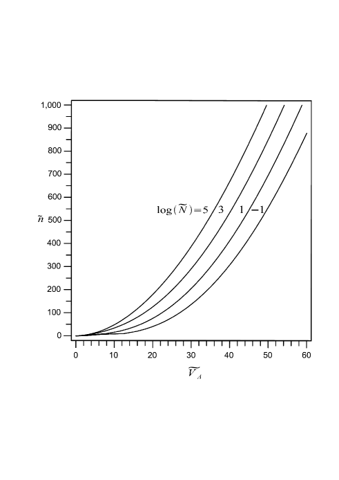
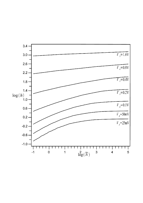
We now use Eqs. (13) and (14) in conjunction with the relation to eliminate the potential components and , and to evaluate the reduced density of doped charge carriers in graphene, , as a function of the reduced applied voltage and the reduced salt concentration . The results are shown in Figs. 1 and 2, covering the following ranges: (corresponding to cm-2), (corresponding to 1.6 V), and (corresponding to M 0.18 M). In Fig. 1 one notices a strong dependence of on the applied potential for greater than about 30, which gives approximately equal rates of change for each salt concentration at the highest values of the applied potential. On the other hand, at the lower applied potential values, there exists a much stronger dependence on the salt concentration, which is revealed in Fig. 2, showing versus for several applied voltages. Indeed, one notices a very strong sensitivity of the doped charge carrier density in graphene to the salt concentration for applied voltages 0.4 V in the range of salt concentrations 1 mM. Even though this sensitivity seems to be the strongest at the lowest applied voltages, one should bear in mind that the electrical conductivity in graphene becomes rather uncertain around its minimum value, which extends up to doping densities about cm-2 Tan_2007 ; Adam_2009 . Therefore, it seems that V would be an optimal range of applied voltages for sensor applications of the electrolytically top gated graphene in probing salt concentrations in the sub-microMole range.
Next, moving to the capacitance of electrolytically top gated graphene, , we note that the reduced capacitances, and , are obtained from Eqs. (3) and (10) as
| (15) |
| (16) |
showing that and are comparable in magnitude for vanishing potentials when the salt concentration is . Moreover, referring to Eq. (9) as an electrical model where graphene and the EDL act as a series connection of capacitors, it follows that graphene’s quantum capacitance will be promoted as the dominant contribution to the total gate capacitance as the salt concentration increases.
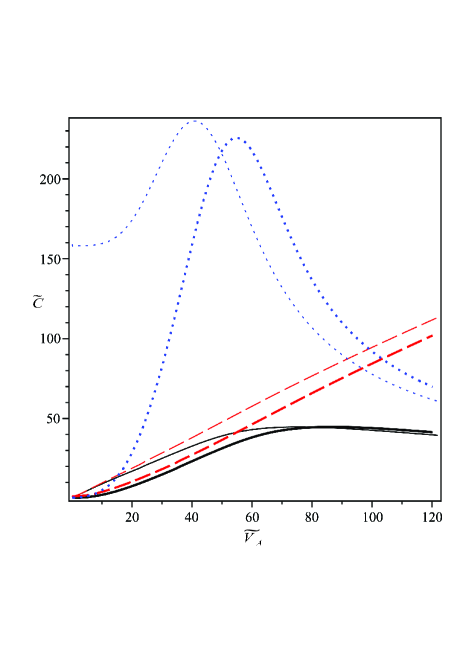
We now use the equality of the right-hand-sides in Eqs. (13) and (14) along with the relation to eliminate and , and to evaluate the reduced quantum capacitance of graphene from Eq. (15), as well as the reduced capacitance of the EDL from Eq. (16) as functions of the reduced applied voltage . Results are shown in Fig. 3 along with the total reduced capacitance of the system based on Eq. (9), for two reduced salt concentrations, = 1 and (corresponding to 1.8 M and 0.18 M, respectively). We show our results for the reduced applied voltages up to 120 in order to elucidate the effect of saturation in the total capacitance that occurs at 85 V (corresponding to 2.21 V) for and at 75 (corresponding to 1.95 V) for . As can be seen from dotted curves in Fig. 3, showing a non-monotonous dependence of the EDL capacitance on the applied voltage, the saturation effect in the total capacitance of the electrolytically top gated graphene is a consequence of the steric effect of the electrolyte ions that are crowded at the graphene surface at high applied voltages Kilic_2007 . Even though the voltages where the saturation occurs are relatively high, they may still be accessible in experiments on graphene. Furthermore, we see in Fig. 3 that, at intermediate applied voltages, the rate of change of the total capacitance follows closely that of the quantum capacitance, with the value 23 F/(V cm2) that is commensurate with recent measurement Xia_2009 . At the lowest applied voltages, one notices in Fig. 3 a “rounding” of the total capacitance as a function of voltage for low salt concentrations, which comes from the EDL capacitance. Such rounding is observed in the recent experiment Xia_2009 .
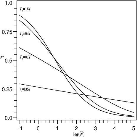
As a consequence of the vast differences between the capacitances shown in Fig. 3, one expects that there exists a broad variation in the way how is the total applied voltage split between the potential drop across the EDL and the voltage pertaining to the change in graphene’s chemical potential. We therefore display in Fig. 4 the variation of the fraction as a function of the reduced salt concentration in the electrolyte for several values of the applied voltage . One can see that, at low salt concentrations, the potentials and are roughly comparable in magnitude, although the ratio increases in favor of the potential drop across the electrolyte as the applied voltage increases. However, this trend is reversed at high salt concentrations and, more importantly, Fig. 4 shows that most of the applied voltage is used to increase graphene’s chemical potential for a full range of applied voltages when salt concentration exceeds, say, mM. Besides its importance for applications, the fact that the potential drop across the electrolyte remains very small at high applied voltages also alleviates concern that a high electric filed in the electrolyte may cause the onset of voltage-dependent electrochemical reactions on graphene.
IV Concluding remarks
We have analyzed the doping of single-layer graphene due to application of the gate potential through an aqueous solution of salt using a modified Poisson-Boltzman model for electrolyte, and found great sensitivity of the induced charge density in graphene to the broad ranges of both salt concentration and applied voltage. We have further analyzed differential capacitance of the electrolytically top gated graphene, and found that its quantum capacitance is promoted as the dominant component owing to a reduction in the Debye length of the electric double layer when the salt concentration increases. In this case, very little potential drop appears across the electrolyte, and graphene takes most of the voltage drop to shift its chemical potential. These findings have several important consequences.
First, since graphene’s conductivity is dependent upon its chemical potential via doping density, Eq. (1), the sensitivity of the latter to the salt concentration implies good prospects for applications in biochemical sensors, especially for in-vivo electrochemical measurements in biological systems owing to graphene’s natural bio-compatibility. Next, since most of the applied voltage can be used to increase the chemical potential of graphene, as opposed to a potential drop across the electrolyte, one can envision ways to use a very thin top gate (in the form of a liquid or solid electrolyte) that requires relatively low gate voltage to change the chemical potential (and hence conductivity) of graphene in future small scale field effect devices with tunable conductivity. Among other aspects of the increased role of graphene’s quantum capacitance is reduction of the electrical field across the electrolyte. This can help reduce the rates of voltage-induced electrochemical reactions on graphene’s surface, as well as improve the mobility of charge carriers in graphene by reducing their scattering rates on various impurities. Moreover, since quantum capacitance is basically the capacitance associated with change in carrier densities in graphene, it can be seen as analogous to the junction capacitance, and the smaller quantum capacitance could in turn lead to faster switching time for graphene based devices.
Many of these advantages of top gating through an electrolyte are related to a high bulk dielectric constant of the electrolyte, especially in aqueous solutions. So, even though the oxide thickness can be reduced down to around 2nm in the present generation conventional MOS structures, the much higher dielectric constant of water in comparison to SiO2 should provide for a higher gate capacitance, translating into much better field effect performance, as discussed above. However, dielectric constant of an electrolyte can be significantly reduced close to a charged surface Kornyshev_2007 ; Abrashkin_2007 , and this issue has yet to be discussed in the context of electrolytic top gating of carbon nano-structures.
Acknowledgements.
This work was supported by the Natural Sciences and Engineering Research Council of Canada.References
- (1) Kong J, Franklin NR, Zhou CW, Chapline MG, Peng S, Cho KJ, Dai HJ, 2000, Nanotube molecular wires as chemical sensors, Science 287, 622.
- (2) Kauffman DR, Star A, 2008, Electronically monitoring biological interactions with carbon nanotube field-effect transistors, Chem. Soc. Reviews 37, 1197.
- (3) Schedin F, Geim AK, Morozov SV, Hill EW, Blake P, Katsnelson MI, Novoselov KS, 2007, Detection of individual gas molecules adsorbed on graphene, Nature Materials 6, 652.
- (4) Robinson JT, Perkins FK, Snow ES, Wei ZQ, Sheehan PE, 2008, Reduced Graphene Oxide Molecular Sensors, Nano Lett. 8, 3137.
- (5) Ang PK, Chen W, Wee ATS, Loh KP, 2008, Solution-Gated Epitaxial Graphene as pH Sensor, J. Am. Chem. Soc. 130, 14392.
- (6) Das A, Pisana S, Chakraborty, Piscanec S, Saha SK, Waghmare UV, Novoselov KS, Krishnamurthy HR, Geim AK, Ferrari AC, Sood AK, 2008, Monitoring dopants by Raman scattering in an electrochemically top-gated graphene transistor, Nature Nanotechnology 3, 210.
- (7) Kruger M, Buitelaar MR, Nussbaumer T, Schonenberger C, Forro L, 2001, Electrochemical carbon nanotube field-effect transistor, Appl. Phys. Lett. 78, 1291.
- (8) Rosenblatt S, Yaish Y, Park J, Gore J, Sazonova V, McEuen PL, 2002, High performance electrolyte gated carbon nanotube transistors, Nano Lett. 2, 869.
- (9) Heller I, Kong J, Williams KA, Dekker C, Lemay SG, 2006, Electrochemistry at single-walled carbon nanotubes: The role of band structure and quantum capacitance, J. Am. Chem. Soc. 128, 7353.
- (10) Chen F, Xia JL, Tao NJ, 2009, Ionic Screening of Charged-Impurity Scattering in Graphene, Nano Lett. 9, 1621.
- (11) Xia JL, Chen F, Li JH, Tao NJ, 2009, Measurement of the quantum capacitance of graphene, Nature Nanotechnology 5, in press, doi:10.1038/nnano.2009.177
- (12) Castro Neto AH, Guinea F, Peres NM, Novoselov KS, Geim AL, 2009, The electronic properties of graphene, Rev. Mod. Phys. 81, 109.
- (13) Bard AJ, Faulkner LR, Electrochemical Methods: Fundamentals and Applications, (Willey, 2001).
- (14) Fang T, Konar A, Xing HL, Jena D, 2007, Carrier statistics and quantum capacitance of graphene sheets and ribbons, Appl. Phys. Lett. 91, 092109.
- (15) Guo J, Yoon Y, Ouyang Y, 2007, Gate electrostatics and quantum capacitance of graphene nanoribbons, Nano Lett. 7, 1935.
- (16) Giannazzo F, Sonde S, Raineri V, Rimini E, 2009, Screening Length and Quantum Capacitance in Graphene by Scanning Probe Microscopy, Nano Lett. 9, 23.
- (17) Sonde S, Giannazzo F, Raineri V, Rimini E, 2009, Dielectric thickness dependence of capacitive behavior in graphene deposited on silicon dioxide, J. Vac. Sci. Technol. B 27, 868.
- (18) Ponomarenko LA, Yang R, Mohiuddin TM, Katsnelson MI, Novoselov KS, Morozov SV, Zhukov AA, Schedin F, Hill EW, Geim AK, 2009, Effect of a High-kappa Environment on Charge Carrier Mobility in Graphene, Phys. Rev. Lett. 102, 206603.
- (19) Borukhov I, Andelman D, Orland H, 1997, Steric effects in electrolytes: A modified Poisson-Boltzmann equation, Phys. Rev. Lett. 79, 435.
- (20) Kilic MS, Bazant MZ, Ajdari A, 2007, Steric effects in the dynamics of electrolytes at large applied voltages. I. Double-layer charging, Phys. Rev. E 75, 021502.
- (21) Radovic I, Hadzievski Lj, Miskovic ZL, 2008, Polarization of supported graphene by slowly moving charges, Phys. Rev. B 77, 075428.
- (22) Fernandez-Rossier J, Palacios JJ, Brey L, 2007, Electronic structure of gated graphene and graphene ribbons, Phys. Rev. B 75, 205441.
- (23) Abramowitz M, Stegun IA, Handbook of Mathematical Functions, (National Bureau of Standards, Washington, 1965).
- (24) Kornyshev AA, 2007, Double-layer in ionic liquids: Paradigm change, J. Phys. Chem B 111, 5545.
- (25) Abrashkin A, Andelman D, Orland H, 2007, Dipolar Poisson-Boltzmann equation: Ions and dipoles close to charge interfaces, Phys. Rev. Lett. 99, 077801.
- (26) Tan YW, Zhang Y , Bolotin K, Zhao Y , Adam S, Hwang EH , Das Sarma S, Stormer HL, Kim P, 2007, Measurement of scattering rate and minimum conductivity in graphene, Phys. Rev. Lett. 99, 246803.
- (27) Adam S, Hwang EH, Rossi E, Das Sarma S, 2009, Theory of charged impurity scattering in two-dimensional graphene, Solid State Communications 149, 1072.