Vertical absorption edge and universal onset conductance in semi-hydrogenated graphene
Abstract
We show that for graphene with any finite difference in the on-site energy between the two sub-lattices (), The optical absorption edge is determined by the . The universal conductance will be broken and the conductance near the band edge varies with frequency as . Moreover, we have identified another universal conductance for such systems without inversion symmetry, i.e., the onset conductance at the band edge is , independent of the size of the band gap. The total integrated optical response is nearly conserved despite of the opening of the band gap.
pacs:
73.50.Mx, 78.67.-n, 81.05.UwIn recent years, graphene has attracted a great deal of interestnovo1 ; novo2 ; zhang1 ; berg . New physics have been predicted and observed, such as electron-hole symmetry and half-integer quantum Hall effectnovo2 ; zhang1 , finite conductivity at zero charge-carrier concentrationnovo2 , and the strong suppression of weak localizationsuzuura ; morozov ; khveshchenko . In graphene, the conduction and valence bands touch each other at six equivalent points, the and points in the Brillouin zone. Near these points the electrons behave like massless Dirac Fermions. One of the most striking features of the massless Dirac Fermion is that the optical conductance is a universal constant, . This was calculated theoretically long before graphene’s fabrication in 2003 early_universal . In the visible region of the electromagnetic spectrum, the absorption coefficient and transmittance of graphene have been measured experimentally and the universal conductance has been confirmedgus ; kuz ; nair .
The optical conductivity of graphene outside the low energy Dirac regime has been calculated theoreticallyChao-Ma ; peres_OC . Outside the Dirac regime the band bending results in an increased density of states. As a result the optical response increases and reaches a sharp maximum at the van Hove point of where is the electronic energy and eV is the hopping bandwidth. The nearly total transparency of graphene can be partially alleviated in the case of bilayer grapheneOCBLG . The problem is even further alleviated in the case of single layer graphene nanoribbons in a magnetic field where the conductance can be as much as two orders of magnitude higher than that for grapheneliu1 , and recently it was shown that a subclass of bilayer nanoribbons is similarly active in the THz-FIR regime even without a magnetic field OCBLGNR .
Graphene was predicted and later experimentally confirmed to undergo metal-semiconductor transition when fully hydrogenated (graphane). Hydrogenated graphene loses the symmetry of A and B sublattices. It can posses magnetic order and becomes ferromagneticzhou . Graphene systems with broken inversion symmetry are of direct experimental interest. Observation of a band gap opening in epitaxial graphene has been reportedzhou1 . This is a direct consequense of the inversion symmetry breaking by the substrate potentialgwo . A scheme to detect valley polarization in graphene systems with broken inversion symmetry was demonstratedniu . In this paper, we shall show that due to the inequivalence of the two valleys, the universal conductance breaks down at low frequencies. If the on-site energy difference of the two sublattice is , absorption is only possible for frequencies above . The conductance at the absorption edge is twice the universal conductance, drops slowly as . Therefore the universal conductance is only approximately valid in a narrow regime overlapping with the visible band.
In the tight-binding approximation, the Hamiltonian for the graphene can be written as,
| (1) |
where , is the next nearest neighbor coupling, and . and are unit vectors given as .
In the Hamiltonian, the on-site energies of the A-sublattice and B-sublattice are and , respectively. The eigenvalues are
| (2) |
with . Correspondingly, the eigenstates can be written in the form of
| (3) |
with
| (4) |
where . The velocity operator can be obtained by and is independent of ,
where and .
The second quantized current density operator is given by
| (5) |
The optical conductivity can be calculated from the Kubo formula,
| (6) |
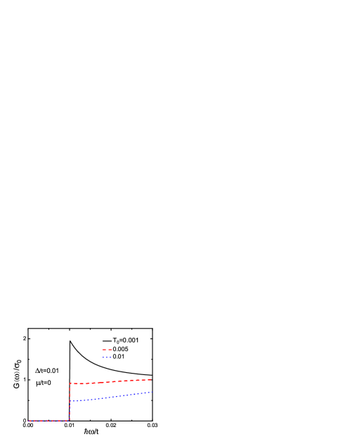
In Fig.1, we plot the optical conductance versus frequency for a typical value of . The A-B on-site energy difference removes the universal conductance which is the key feature of graphene with A-B symmetry. For , the conductance is zero for any temperature since only vertical transitions are allowed. For , thermal excitation will reduce the carrier concentration near the top of the valence band and the total interband transition rate decreases. As a result, the conductance decreases as temperatures increases. At the frequencies close to the energy gap, the conductance jumps to a maximum which is greater than the universal conductance.
where and is the inverse temperature in energy units. The conductance then decreases slowly as the joint density of states for optical transition decreases.
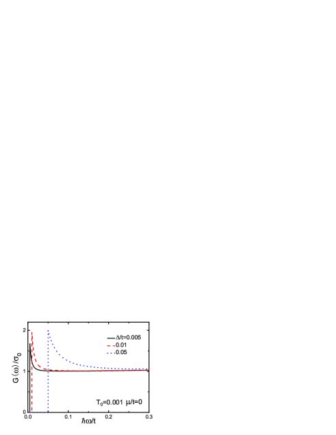
The low frequency conductance for difference values of is shown in Fig.2. The onset conductance decreases as decreases. For systems with complete A-B symmetry, the onset maximum disappears. In this case the conductance starts from the universal conductance at and from zero at finite temperature. The conductance at is . Therefore, it is found that for , the conductance at is regardless of the value of .
At relatively low energy around the Dirac points, , and , where is measured from the -point. In this region, the conductance is isotropic, , given as,
| (7) | |||||
Here, ,
In Fig.3, we show the zero temperature conductance over a wide frequency range of to . The absorption at frequencies below the gap is now forbidden, as expected. The interesting feature of this systems is the onset of absorption at the band edge. The absorption at the edge is discontinuous and jumps vertically from zero to a value twice the universal conductance. This behavior can be derive analytically around the Dirac regime as follows.
In the limit of , , we obtain a simple form for the conductance due to the contribution from the 6 Dirac points, given as . At for any , the conductance is twice of the universal conductance. In other words, for graphene with A-B asymmetry, while the universal conductance is broken, the onset conductance at the band edge for has a universal value of . In comparison to the wellknown interband absorption rate in semiconductors, , this feature of interband absorption in graphene is very unique. At higher frequency, the conductance increases with frequency. Therefore an inequivalence of A-B sublattices can remove the universal conductance, or limit its applicability to a small regime around the visible frequency.
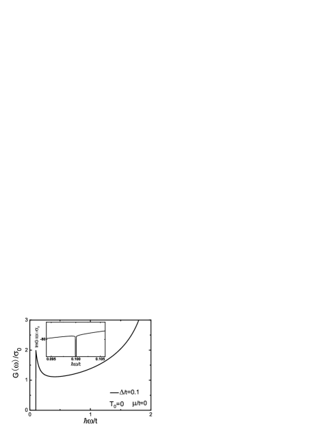
The inset of Fig.3 shows the imaginary part of the conductivity. Near the band edge, the imaginary part is very large which indicate phase difference of nearly between the incident field and the current response. This phase difference decreases rapidly as frequency increases. The size of the dip at is about the same order of magnitude as the jump in the conductance.
The total integrated absorption is given by
| (8) |
Experimentallynair it has been shown that for graphene with A-B symmetry, the universal conductance is valid up to the high end of the visible band, or . Theoretically it is shown that the conductance is approximately up to . Therefore for graphene with A-B symmetry, we integrate (10) from 0 to and . For graphene without A-B symmetry, we integrate (10) from to and . Since , we can conclude that the total optical response is nearly conserved even when a gap opens up at the Fermi energy. For small , any loss of optical response due to the gap is recovered in the regime of slightly higher than . For large , the region required for recovering the optical response is wider. This can be seen quantitatively in Fig.2.
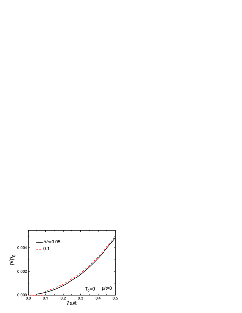
Finally we show in Fig.4 that the resistivity of the system, defined as , has a well behaved monotonic frequency dependence. Apart from a small jump at the band gap, the resistivity varies with frequency approximately parabolically below the van Hove point.
In conclusion, we have shown that for graphene without inversion symmetry the optical conductance becomes strongly frequency dependent. However, the onset conductance at the band edge has a universal value, regardless of the value the band gap.
Acknowledgement– This work is supported in part by the National Natural Science Foundation of China and the Australian Research Council.
a)Electronic mail: leichen@pku.edu.cn
b)Electronic mail: czhang@uow.edu.au
References
- (1) K.S. Novoselov, A.K. Geim, S.V. Morozov, D. Jiang, Y. Zhang, S.V. Dubonos, I.V. Grigorieva, A.A. Firsov, Science 306, 666 (2004).
- (2) K.S. Novoselov, A.K. Geim, S.V. Morozov, D. Jiang, M.I. Katsenelson, I.V. Grigorieva, S.V. Dubonos, A.A. Firsov, Nature (London) 438, 197 (2005).
- (3) Y. Zhang, Y.W. Tan, H.L. Stormer, P. Kim, Nature (London) 438, 201 (2005).
- (4) C. Berger, Z. Song, X. Li, X. Wu, N. Brown, C. Naud, D. Mayou, T. Li, J. Hass, A. N. Marchenkov, E. H. Konrad, P. N. First, W. A. de Heer, Science 312, 1191 (2006).
- (5) H. Suzuura, T. Ando, Phys. Rev. Lett. 89, 266603 (2002).
- (6) S.V. Morozov, K.S. Novoselov, M.I. Katsnelson, F. Schedin, L.A. Ponomarenko, D. Jiang, A.K. Geim, Phys. Rev. Lett. 97, 016801 (2006).
- (7) D.V. Khveshchenko, Phys. Rev. Lett. 97, 36802 (2006).
- (8) E. Fradkin, Phys. Rev. B 33, 3263 (1986).
- (9) V.P. Gusynin, S.G. Shrapov, J.P. Carbotte, Phys. Rev. Lett. 96, 56802 (2006).
- (10) A. B. Kuzmenko, E. van Heumen, F. Carbone, D. van der Marel, Phys. Rev. Lett., 100, 117401 (2008).
- (11) R. R. Nair, P. Blake, A. N. Grigorenko,K. S. Novoselov, T. J. Booth, T. Stauber, N. M. R. Peres, A. K. Geim, Science 320, 1308 (2008).
- (12) C. Zhang, L. Chen, Z. Ma, Phys. Rev. B, 77 241402 (2008).
- (13) T. Stauber, N. M. R. Peres, A. K. Geim, Phys. Rev. B, 78 085432 (2008).
- (14) A.R. Wright, F.Liu, C. Zhang, Nanotechnology 20, 405203 (2009)
- (15) J. Liu, A.R. Wright, C. Zhang, and Z. Ma, App. Phys. Lett., 93, 041106 (2008).
- (16) A.R. Wright, J.C. Cao, C.Zhang, arXiv:0905.4304.
- (17) J. Zhou, Q. Wang, Q. Sun, X. S. Chen, Y. Kawazoe, and P. Jena, Nano Lett. 9, DOI: 10.1021/nl9020733, (2009).
- (18) S.Y. Zhou et al., Nat. Mater. 6, 770 (2007).
- (19) S. Gwo and C. K. Shih, Phys. Rev. B 47, 13059 (1993).
- (20) D. Xiao, W. Yao, Q. Niu, Phys. Rev. Lett. 99, 236809 (2007)