Quantum transport in a mesoscopic ring:
Evidence of an OR gate
Santanu K. Maiti1,2,∗
1Theoretical Condensed Matter Physics Division,
Saha Institute of Nuclear Physics,
1/AF, Bidhannagar, Kolkata-700 064, India
2Department of Physics, Narasinha Dutt College,
129, Belilious Road, Howrah-711 101, India
Abstract
We explore OR gate response in a mesoscopic ring threaded by a magnetic flux . The ring is symmetrically attached to two semi-infinite one-dimensional metallic electrodes and two gate voltages, viz, and , are applied in one arm of the ring which are treated as the two inputs of the OR gate. All the calculations are based on the tight-binding model and the Green’s function method, which numerically compute the conductance-energy and current-voltage characteristics as functions of the gate voltages, ring-to-electrodes coupling strengths and magnetic flux. Our theoretical study shows that, for (, the elementary flux-quantum) a high output current () (in the logical sense) appears if one or both the inputs to the gate are high (), while if neither input is high (), a low output current () appears. It clearly demonstrates the OR gate behavior and this aspect may be utilized in designing the electronic logic gate.
PACS No.: 73.23.-b; 73.63.Rt.
Keywords: A. Mesoscopic ring; D. Conductance; D. - characteristic; D. OR gate.
∗Corresponding Author: Santanu K. Maiti
Electronic mail: santanu.maiti@saha.ac.in
1 Introduction
The study of electron transport in quantum confined model system is a challenging field in the modern age of nanoscience and technology, since these simple looking systems can be used to design nanodevices especially in electronic as well as spintronic engineering. A mesoscopic metallic ring is a nice example of quantum confined systems, and, with the help of the ring we can make a device that can act as a logic gate, which may be used in nanoelectronic circuits. To reveal this phenomenon we design a bridge system where the ring is attached to two external electrodes, the so-called electrode-ring-electrode bridge. Based on the pioneering work of Aviram and Ratner [1], the theoretical description of electron transport in a bridge system has got much progress. Later, many excellent experiments [2, 3, 4] have been done in several bridge systems to understand the basic mechanisms underlying the electron transport. Though in literature both theoretical [5, 6, 7, 8, 9, 10, 11, 12, 13, 14, 15, 16] as well as experimental [2, 3, 4] works on electron transport are available, yet lot of controversies are still present between the theory and experiment, and the complete knowledge of the conduction mechanism in this scale is not very well established even today. The ring-electrodes interface structure significantly controls the electronic transport in the ring. By changing the geometry, one can tune the transmission probability of an electron across the ring which is solely due to the effect of quantum interference among the electronic waves passing through different arms of the ring. Furthermore, the electron transport in the ring can be modulated in other way by tuning the magnetic flux, the so-called Aharonov-Bohm (AB) flux, that threads the ring. The AB flux threading the ring may change the phases of the wave functions propagating along the different arms of the ring leading to constructive or destructive interferences, and therefore, the transmission amplitude changes [17, 18, 19, 20, 21]. Beside these factors, ring-to-electrodes coupling is another important issue that controls the electron transport in a meaningful way [21]. All these are the key factors which regulate the electron transmission in the electrode-ring-electrode bridge system and these effects have to be taken into account properly to reveal the transport mechanisms.
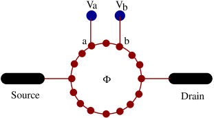
Our main focus of the present paper is to describe the OR gate response in a mesoscopic ring threaded by a magnetic flux . The ring is contacted symmetrically to the electrodes, and the two gate voltages and are applied in one arm of the ring (see Fig. 1) those are treated as the two inputs of the OR gate. Here we adopt a simple tight-binding model to describe the system and all the calculations are performed numerically. We address the OR gate behavior by studying the conductance-energy and current-voltage characteristics as functions of the ring-electrodes coupling strengths, magnetic flux and gate voltages. Our study reveals that for a particular value of the magnetic flux, , a high output current () (in the logical sense) is available if one or both the inputs to the gate are high (), while if neither input is high (), a low output current () appears. This phenomenon clearly demonstrates the OR behavior. To the best of our knowledge the OR gate response in such a simple system has not been addressed earlier in the literature.
We organize the paper as follow. Following the introduction (Section ), in Section , we present the model and the theoretical formulations for our calculations. Section discusses the results, and finally, we summarize our results in Section .
2 Model and the theoretical background
We start by referring to Fig. 1. A mesoscopic ring, threaded by a magnetic flux , is attached symmetrically (upper and lower arms have equal number of lattice points) to two semi-infinite one-dimensional (D) metallic electrodes. The atoms and in the upper arm of the ring are subjected to the gate voltages and respectively, and these are treated as the two inputs of the OR gate.
Using the Landauer conductance formula [22, 23] we calculate the conductance () of the ring. At very low temperature and bias voltage it can be expressed in the form,
| (1) |
where gives the transmission probability of an electron through the ring. This can be represented in terms of the Green’s function of the ring and its coupling to the two electrodes by the relation [22, 23],
| (2) |
where and are respectively the retarded and advanced Green’s functions of the ring including the effects of the electrodes. The parameters and describe the coupling of the ring to the source and drain respectively. For the full system i.e., the ring, source and drain, the Green’s function is defined as,
| (3) |
where is the injecting energy of the source electron. To Evaluate this Green’s function, the inversion of an infinite matrix is needed since the full system consists of the finite ring and the two semi-infinite electrodes. However, the entire system can be partitioned into sub-matrices
corresponding to the individual sub-systems and the Green’s function for the ring can be effectively written as,
| (4) |
where is the Hamiltonian of the ring that can be expressed within the non-interacting picture like,
| (5) | |||||
In this Hamiltonian ’s are the site energies for all the sites except the sites and where the gate voltages and are applied, those are variable. These gate voltages can be incorporated through the site energies as expressed in the above Hamiltonian. () is the creation (annihilation) operator of an electron at the site and is the nearest-neighbor hopping integral. The phase factor comes due to the flux threaded by the ring, where corresponds to the total number of atomic sites in the ring. Similar kind of tight-binding Hamiltonian is also used, except the phase factor , to describe the D perfect electrodes where the Hamiltonian is parametrized by constant on-site potential and nearest-neighbor hopping integral . The hopping integral between the source and the ring is , while it is between the ring and the drain. The parameters and in Eq. (4) represent the self-energies due to the coupling of the ring to the source and drain respectively, where all the informations of this coupling are included into these self-energies.
To evaluate the current (), passing through the ring, as a function of the applied bias voltage () we use the relation [22],
| (6) |
where is the equilibrium Fermi energy. Here we assume that the entire voltage is dropped across the ring-electrode interfaces, and it is examined that under such an assumption the - characteristics do not change their qualitative features.
All the results in this presentation are computed at absolute zero temperature, but they should valid even for finite temperature ( K) as the broadening of the energy levels of the ring due to its coupling with the electrodes becomes much larger than that of the thermal broadening [22]. For simplicity, we take the unit in our present calculations.
3 Results and discussion
To illustrate the results, let us first mention the values of the different parameters used for the numerical calculations. In the ring, the on-site energy is taken as for all the sites , except the sites and where the site energies are taken as and respectively, and the nearest-neighbor hopping strength is set to . On the other hand, for the side attached electrodes the on-site energy () and the nearest-neighbor hopping strength () are fixed to and respectively. Throughout the study, we focus our results for the two limiting cases depending on the strength of the coupling of the ring to the source and drain. In one case we use the condition , which is the so-called weak-coupling limit. For this regime we choose . In the other case the condition is used, which is named as the strong-coupling limit. In this particular regime, the values of the parameters are set as . The key controlling parameter for all these calculations is the magnetic flux which is set to i.e., in our chosen unit.
As illustrative examples, in Fig. 2 we display the conductance-energy (-) characteristics for a mesoscopic ring considering in the limit of weak ring-to-electrodes coupling,
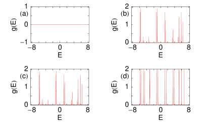
where (a), (b), (c) and (d) correspond to the results for the four different cases of the gate voltages and . In the particular case when i.e., both the inputs are low (), the conductance shows the value in the entire energy range (Fig. 2(a)). This clearly indicates that the electron cannot conduct from the source to the drain across the ring. While, for the other three cases i.e., and (Fig. 2(b)), and (Fig. 2(c)) and (Fig. 2(d)), the conductance shows fine resonance peaks for some particular energies. Thus, in all these three cases, the electron can conduct through the ring. From Fig. 2(d) it is observed that at the resonances the conductance approaches the value , and accordingly, the transmission probability goes to unity, since the relation is satisfied from the Landauer conductance formula (see Eq. 1 with ). On the other hand, the transmission probability decays from for the cases where any one of the two gate voltages is high and other is low (Figs. 2(b) and (c)). All these resonance peaks are associated with the energy eigenvalues of the ring, and therefore, we can say that the conductance spectrum reveals itself the electronic structure of the ring. Now we interpret the dependences of the two gate voltages in these four different cases. The probability amplitude of getting an electron across the ring depends on the quantum interference of the electronic waves passing through the two arms of the ring. For the ring attached symmetrically to the electrodes i.e., when the two arms of the ring are identical with each other, the probability amplitude is exactly zero () for the flux . This is due to the result of the quantum interference among the two waves in the two arms of the ring, which can be obtained in a very simple mathematical calculation. Thus for the cases when both the two inputs ( and ) are zero (low), the two arms of the ring become identical, and therefore, the transmission probability drops to zero. On the other hand, for the other three cases the symmetry of the two arms of the ring
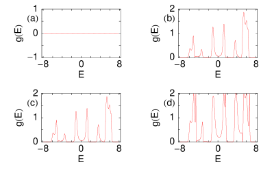
is broken when either the atom or or the both are subjected to the gate voltages and , and therefore, the non-zero value of the transmission probability is achieved which reveals the electron conduction across the ring. The reduction of the transmission probability for the cases when any one of the two gates is high and other is low compared to the case where both the gates are high is also due to the quantum interference effect. Thus we can predict that the electron conduction takes place across the ring if any one or both the inputs to the gate are high, while if both the inputs are low, the conduction is no longer possible. This feature clearly demonstrates the OR gate behavior. In the limit of strong-coupling, we get additional one feature compared to those as presented in the limit of weak-coupling. The results are shown in Fig. 3, where the results in (a), (b), (c) and (d) are drawn respectively for the same gate voltages as in Fig. 2. For the strong-coupling limit, all the resonances get substantial widths compared to the weak-coupling limit. The contribution for the broadening of the resonance peaks in this strong-coupling limit appears from the imaginary parts of the self-energies and respectively [22]. Hence by tuning the coupling strength, we can get the electron transmission across the ring for the wider range of energies and it provides an important signature in the study of current-voltage (-) characteristics.
All these features of electron transfer become much more clearly visible by studying the - characteristics. The current passing through the
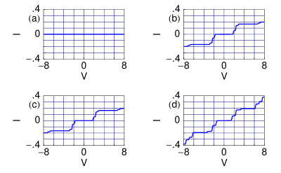
ring is computed from the integration procedure of the transmission function as prescribed in Eq. 6. The transmission function varies exactly similar to that of the conductance spectrum, differ only in magnitude by the factor since the relation holds from the Landauer conductance formula Eq. 1. As representative examples, in Fig. 4 we display the current-voltage characteristics for a mesoscopic ring with in the limit of weak-coupling. For the case when both the two inputs are zero, the current is zero (see Fig. 4(a)) for the
| Input-I () | Input-II () | Current () |
entire bias voltage . This feature is clearly visible from the conductance spectrum, Fig. 2(a), since the current is computed from the integration procedure of the transmission function . In the rest three cases, a high output current is obtained those are clearly presented in Figs. 4(b), (c) and (d). From these figures it is observed that
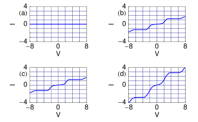
the current exhibits staircase-like structure with fine steps as a function of the applied bias voltage. This is due to the existence of the sharp resonance peaks in the conductance spectrum in the weak-coupling limit, since the current is computed by the integration method of the transmission function . With the increase of the bias voltage , the electrochemical potentials on the electrodes are shifted gradually, and finally cross one of the quantized energy levels of the ring. Accordingly, a current channel is opened up which provides a jump in the - characteristic curve. Addition to these behaviors, it is also important to note that the non-zero value of the current appears beyond a finite value of , the so-called threshold voltage (). This can be controlled by tuning the size () of the ring. From these - characteristics, the OR gate response is understood very easily. To make it much clear, in Table 1, we show a quantitative estimate of the typical current amplitude determined at the bias voltage , in this limit of weak ring-to-electrodes coupling.
| Input-I () | Input-II () | Current () |
It is observed that when any one of the two gates is high and other is low, the current gets the value , and for the case when both the two inputs are high, it () achieves the value . While, for the case when both the two inputs are low (), the current becomes exactly zero. In the same analogy, as above, here we also discuss the - characteristics for the strong-coupling limit. In this limit, the current varies almost continuously with the applied bias voltage and achieves much larger amplitude than the weak-coupling case as presented in Fig. 5. The reason is that, in the limit of strong-coupling all the energy levels get broadened which provide larger current in the integration procedure of the transmission function . Thus by tuning the strength of the ring-to-electrodes coupling, we can achieve very large current amplitude from the very low one for the same bias voltage . All the other properties i.e., the dependences of the gate voltages on the - characteristics are exactly similar to those as given in Fig. 4. In this strong-coupling limit we also make a quantitative study for the typical current amplitude, given in Table 2, where the current amplitude is determined at the same bias voltage () as earlier. The response of the output current is exactly similar to that as given in Table 1. Here the current achieves the value in the cases where any one of the two gates is high and other is low, and it () becomes for the case where both the two inputs are high. On the other hand, the current becomes exactly zero for the case where . The non-zero values of the current in this strong-coupling limit are much larger than the weak-coupling case, as expected. From these results we can clearly manifest that a mesoscopic ring exhibits the OR gate response.
4 Concluding remarks
To summarize, we have addressed the OR gate response in a mesoscopic metallic ring threaded by a magnetic flux and attached symmetrically to the electrodes. Two atoms in the upper arm of the ring are subjected to the gate voltages and respectively those are taken as the two inputs of the OR gate. The system is described by the tight-binding Hamiltonian and all the calculations are done in the Green’s function formalism. We have numerically computed the conductance-energy and current-voltage characteristics as functions of the gate voltages, ring-to-electrodes coupling strengths and magnetic flux. Very interestingly we have noticed that, for the half flux-quantum value of (), a high output current () (in the logical sense) appears if one or both the inputs to the gate are high (). On the other hand, if neither input is high (), a low output current () appears. It clearly manifests the OR behavior and this aspect may be utilized in designing a tailor made electronic logic gate.
In this presentation, we have explored the conductance-energy and current-voltage characteristics for some fixed parameter values considering a ring with total number of atomic sites . Though the results presented here change numerically for the other parameter values and ring size (), but all the basic features remain exactly invariant.
The importance of this article is concerned with (i) the simplicity of the geometry and (ii) the smallness of the size. To the best of our knowledge the OR gate response in such a simple low-dimensional system that can be operated even at finite temperature ( K) has not been addressed in the literature.
References
- [1] A. Aviram and M. Ratner, Chem. Phys. Lett. 29, 277 (1974).
- [2] J. Chen, M. A. Reed, A. M. Rawlett and J. M. Tour, Science 286, 1550 (1999).
- [3] M. A. Reed, C. Zhou, C. J. Muller, T. P. Burgin and J. M. Tour, Science 278, 252 (1997).
- [4] T. Dadosh, Y. Gordin, R. Krahne, I. Khivrich, D. Mahalu, V. Frydman, J. Sperling, A. Yacoby and I. Bar-Joseph, Nature 436, 677 (2005).
- [5] A. Nitzan, Annu. Rev. Phys. Chem. 52, 681 (2001).
- [6] A. Nitzan and M. A. Ratner, Science 300, 1384 (2003).
- [7] P. Földi, B. Molnár, M. G. Benedict and F. M. Peeters, Phys. Rev. B 71, 033309 (2005).
- [8] B. Molnár, F. M. Peeters and P. Vasilopoulos, Phys. Rev. B 69, 155335 (2004).
- [9] P. A. Orellana, M. L. Ladron de Guevara, M. Pacheco and A. Latge, Phys. Rev. B 68, 195321 (2003).
- [10] P. A. Orellana, F. Dominguez-Adame, I. Gomez and M. L. Ladron de Guevara, Phys. Rev. B 67, 085321 (2003).
- [11] D. M. Newns, Phys. Rev. 178, 1123 (1969).
- [12] V. Mujica, M. Kemp and M. A. Ratner, J. Chem. Phys. 101, 6849 (1994).
- [13] V. Mujica, M. Kemp, A. E. Roitberg and M. A. Ratner, J. Chem. Phys. 104, 7296 (1996).
- [14] K. Walczak, Phys. Stat. Sol. (b) 241, 2555 (2004).
- [15] K. Walczak, arXiv:0309666.
- [16] W. Y. Cui, S. Z. Wu, G. Jin, X. Zhao and Y. Q. Ma, Eur. Phys. J. B. 59, 47 (2007).
- [17] R. Baer and D. Neuhauser, J. Am. Chem. Soc. 124, 4200 (2002).
- [18] D. Walter, D. Neuhauser and R. Baer, Chem. Phys. 299, 139 (2004).
- [19] K. Tagami, L. Wang and M. Tsukada, Nano Lett. 4, 209 (2004).
- [20] K. Walczak, Cent. Eur. J. Chem. 2, 524 (2004).
- [21] R. Baer and D. Neuhauser, Chem. Phys. 281, 353 (2002).
- [22] S. Datta, Electronic transport in mesoscopic systems, Cambridge University Press, Cambridge (1997).
- [23] M. B. Nardelli, Phys. Rev. B 60, 7828 (1999).