Correlation-induced conductance suppression at level degeneracy in a quantum dot
Abstract
The large, level-dependent g-factors in an InSb nanowire quantum dot allow for the occurrence of a variety of level crossings in the dot. While we observe the standard conductance enhancement in the Coulomb blockade region for aligned levels with different spins due to the Kondo effect, a vanishing of the conductance is found at the alignment of levels with equal spins. This conductance suppression appears as a canyon cutting through the web of direct tunneling lines and an enclosed Coulomb blockade region. In the center of the Coulomb blockade region, we observe the predicted correlation-induced resonance, which now turns out to be part of a larger scenario. Our findings are supported by numerical and analytical calculations.
Due to their small size the properties of nanosystems are dominated by discrete quantum levels. These levels can be tuned by the means of, e.g., applying a magnetic field. At level crossings a variety of different physical features can arise from electron coherence between the levels as well as correlations with contacts. These can be conveniently probed by transport measurements, see, e.g., Refs. Oosterkamp et al. (1998); Reimann and Manninen (2002); Payette et al. (2009), where generically conductance peaks can be associated with the presence of electronic states at the Fermi level. While most experimental work is done on GaAs-based systems where the individual levels are approximately spin-degenerate due to the small electron g-factor, less results exist at the crossing of spin-resolved levels. Such a level crossing is particularly interesting if both levels are slightly below the Fermi energy, so that there is one electron in the system while a second electron is blocked to enter due to Coulomb repulsion. In this Coulomb blockade region the conductance is typically small. At very low temperatures, however, the Kondo effect provides a strong conductance enhancement at degeneracy of levels with opposite spins as observed in Refs. Goldhaber-Gordon et al. (1998); Cronenwett et al. (1998); Sasaki et al. (2000). For the case of degeneracy of levels with equal spins, much less is known. Here, recent theoretical calculations Meden and Marquardt (2006); Kashcheyevs et al. (2007); Silvestrov and Imry (2007) showed a vanishing conductance at the point of electron-hole symmetry in the middle of the Coulomb blockade region together with the correlation-induced resonance, a strong enhancement of the conductance for slight detuning between the levels.
In this letter, we present detailed measurements on InSb quantum dots realized by electrically contacting epitaxially grown InSb nanowires. These devices exhibit giant, strongly level-dependent electron g-factors Nilsson et al. (2009), which allow for a clear observation of several spin-resolved level crossings at relatively weak magnetic fields, and we can directly compare the results of transport measurements at crossings of levels with equal and different spins. For the case of equal spins we are able to verify the predicted correlation-induced resonance Meden and Marquardt (2006) in the center of the Coulomb blockade region. Furthermore our data shows that this effect is a part of a larger scenario where conductance suppression appears as a line in the parameter space of detuning and gate voltage. These findings are supported by numerical and analytical calculations based on a two-level, equal-spin, interacting model, which fully confirm the observed scenario.
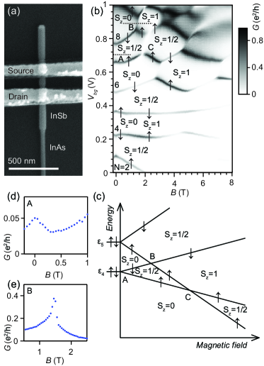
The InSb nanowire dot devices investigated here are fabricated from InSb segments of InAs/InSb heterostructure nanowires where the InAs segments are used as seed nanowires to favor nucleation of InSb Nilsson et al. (2009); Caroff et al. (2008); SuppMat . Figure 1(a) shows a scanning electron microscope (SEM) image of a fabricated device, where the dot is formed between two 150-nm-wide Ti/Au contacts with a distance of 100 nm in an InSb nanowire with a diameter of 65 nm. All measurements are performed in a 3He cryostat at 300 mK.
Figure 1(b) shows a grey-scale plot of the conductance, , as a function of the magnetic field and the back-gate voltage applied to the Si substrate of a fabricated device. The spin state of the last filled electron in each energy level is indicated by an arrow in the figure. Here negative values of the g-factor are assumed for all quantum levels Isaacson (1968). From the magnetic field evolutions of the conductance peaks, we can evaluate the electron g-factors for the dot levels (following Refs. Roddaro et al. (2008); Larsson et al. (2009)) and find that the values of these g-factors are giant, with the largest absolute value reaching about 60, and are strongly level-dependent (see also Refs. Nilsson et al. (2009); SuppMat ). A large difference between the electron g-factors in the dot allows for the crossings of the spin-up state of the 5th level with both the spin-down and the spin-up state of the 4th level as is increased. Figure 1(c) shows a schematic for the scenario of such single-particle level crossings without taking level interaction and the effect of Coulomb charging into account.
The transport measurements in Fig. 1(b) display several clear signatures of both the conventional spin-1/2 Kondo and the integer-spin Kondo-like effects which manifest themselves as conductance enhancements in the Coulomb blockade regions in the InSb quantum dot. For example a weak but visible conductance ridge is observed at zero magnetic field inside the Coulomb blockade region. A line plot of the conductance as a function of the magnetic field along cut A is shown in Fig. 1(d). Here one can easily identify a conductance peak at zero magnetic field. This peak occurs at the standard spin-degeneracy point of level 4 of the quantum dot at as indicated by label A in the schematic shown in Fig. 1(c). Similar conductance peaks or ridges in odd-number electron Coulomb blockade regions are observed in several other fabricated InSb quantum dots at zero magnetic field. All of these conductance enhancements can be attributed to the conventional spin-1/2 Kondo effect Goldhaber-Gordon et al. (1998); Cronenwett et al. (1998).
In addition to the spin-1/2 Kondo effect we see clear signatures of integer-spin Kondo-like correlations Sasaki et al. (2000); Nygård et al. (2000). One such example is provided by the clear high-conductance ridge in the Coulomb blockade region at T [see Fig. 1(b)]. A corresponding line plot of the conductance as a function of the magnetic field along the cut B through the conductance ridge is shown in Fig. 1(e), where a conductance peak is clearly observed. This peak occurs at the degeneracy of levels 4 and 5 with opposite spins as indicated by label B in the schematic shown in Fig. 1(c). An additional, though weaker, integer-spin Kondo-like conductance enhancement is observed in the Coulomb blockade region at T. Such integer-spin Kondo-like conductance enhancements appear at the transition from a spin singlet to the state of an spin triplet as the magnetic field increases. Note that the other states of the triplet are significantly higher in energy due to the large g-factors. Thus more complex phenomena such as the two-stage Kondo effect van der Wiel et al. (2002); Pustilnik and Glazman (2001) are not observed here. Both the spin-1/2 and the integer spin Kondo-like enhancements of the conductance in the Coulomb blockade region occur when there are two degenerate states of different spins.
We now focus our attention to the Coulomb blockade region at magnetic fields of T [Fig. 1(b)] where the 4th and the 5th level with the same spin cross as indicated by label C in the schematic shown in Fig. 1(c). Here we observe a clear suppression of the conductance within the cotunneling background in the Coulomb blockade region. Moreover the direct tunneling lines are also broken at the crossing points at the corners of the Coulomb blockade region. This scenario is shown in detail in Fig. 2(a).
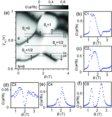
The bright region of the conductance suppression resembles a canyon which connects the upper and Coulomb blockade region with the lower and region while cutting through both the direct tunneling lines and the and blockade region. As shown in Figs. 2(b)-2(f) for different gate voltages, the conductance drops approximately down to zero at the bottom of the canyon. In addition, the conductance in the middle of the Coulomb blockade region [Fig. 2(d)] shows a clear enhancement on both sides of the conductance suppression. This is the correlation-induced resonance, which was predicted for a similar, strong correlated quantum dot system near the electron-hole symmetry point Meden and Marquardt (2006).
This canyon of conductance suppression is the main finding of our letter. We note that the presence of giant, strongly level-dependent g-factors in our InSb nanowire dot is crucial to create the degeneracy between the two spin-up levels at a moderate magnetic field. Furthermore, the quadratic shifts of the levels with magnetic field differ strongly for levels 4 and 5, which has helped to create this desired degeneracy point. Intuitively, the phenomenon of the conductance suppression can be understood as a result of (i) the strong modification of the dot states by correlations with the contacts and (ii) the consequent (destructive) interference between the two paths through the dot associated with the two modified states. This is straightforwardly seen in the lower and upper direct tunneling regions, see the Breit-Wigner results below. However, in the Coulomb blockade region, strong correlations between contacts and the dots states exist, which can result in vanishing conductance at the electron-hole symmetry point at zero temperature and zero bias Meden and Marquardt (2006); Kashcheyevs et al. (2007); Silvestrov and Imry (2007). The observed canyon of conductance suppression connects both scenarios and suggests that the combination of correlations and interference is required for a full understanding.
In the following we show theoretically that a crossing between two levels with equal spins indeed provides a canyon of conductance suppression that cuts through both the Coulomb blockade and direct tunneling regions. Our Hamiltonian combines the terms describing the quantum dot and its coupling to the left (L) and right (R) lead which read (similar to Refs. Meden and Marquardt (2006); Kashcheyevs et al. (2007); Silvestrov and Imry (2007))
| (1) | |||||
| (2) | |||||
where and are the annihilation (creation) operators of electrons in the dot and leads, respectively. We define , which is assumed to be constant, and . Fitting to the conductance peaks SuppMat , we obtain , meV, meV, meV, meV, and the level energies of and . Here, the gate level energy corresponds to the back gate voltage by . (This choice of provides electron-hole symmetry around T at .) As motivated below, we use and , which might reflect a parity difference between the fourth and fifth quantum orbital states. The occupations of the left and right leads are given by Fermi functions with the electrochemical potentials of , respectively.
For , at most one of the two levels is occupied and Coulomb interaction plays no role. In such a non-interacting system, the transmission can be calculated with Green’s functions (GF), see, e.g., Ref. Shahbazyan and Raikh (1994) where a similar system was treated. The finite bias conductance reads for zero temperature, see the black solid line in Fig. 3(a), which agrees well with the data (crosses) from Fig. 2(f). Figure 3(b) shows that the experimental canyon of conductance suppression is reproduced very well by the GF model in its range of validity, . Here the vanishing conductance can be attributed to interference between the transmission through both levels. The Breit-Wigner formula provides
| (3) |
We find the vanishing of at assuming . For our parameters this provides in good agreement with the numerical findings and the experimental data shown in Fig. 3(b). This justifies our choice of .
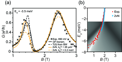
In the Coulomb blockade region () the current is carried by cotunneling events. Here we apply the second-order von Neumann (2vN) approach Pedersen and Wacker (2005), which treats all interactions in exactly. Correlated transitions between the leads and the dot states are included in second order describing cotunneling Pedersen and Wacker (2010) and interference Pedersen et al. (2009). For meV, the results agree excellently with the experimental data, see Fig. 3(a). The 2vN is only reliable above Pedersen and Wacker (2005) which we estimate to be meV SuppMat and we attribute the occurrence of some slightly negative conductivities to the improper treatment of higher-order processes. In order to reduce these problems we use the increased temperature of meV in the following. The results of the calculation are given in Fig. 4(a) and show the canyon of conductance suppression in good agreement with the experiment.
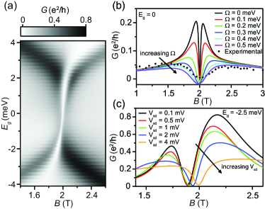
The calculated conductance shows an approximate symmetry around the electron-hole symmetry point (full symmetry is restored by reversing the bias). In contrast, the experimental data are more asymmetric, which indicates a gate voltage dependence of system parameters. Figure 4(b) shows that the conductance suppression persists for a finite interlevel coupling described by an additional term to in Eq. (1), while its width increases. Comparing with experimental data, meV fits better at mV. Even higher values of seem appropriate for larger (not shown), while fits well for mV (see Fig. 3). This indicates that the interlevel coupling depends on the back-gate voltage in our dot and vanishes accidentally around mV. Finally, Fig. 4(c) shows that the vanishing of the current persists for higher biases. In the high-bias limit with infinite this corresponds to the situation discussed in Ref. Li et al. , where it was shown that the current vanishes exactly at level degeneracy (i.e., at in our case), independently of the couplings unless .
In conclusion we have observed that the crossing of quantum levels with equal spins in the presence of Coulomb repulsion manifests as a canyon of vanishing conductance cutting through the direct tunneling lines and the enclosed Coulomb blockade region. This scenario is well covered by the 2vN approach based on a two-level, equal-spin, interacting model. Furthermore, our experimental data confirms the predicted correlation-induced resonances close to the electron-hole symmetry point. Our results show that a full understanding of the interplay between strong correlations and interference is required to describe the entire behavior of the conductance of the system at degeneracy of levels with equal spins.
Acknowledgements.
We thank Karsten Flensberg and Feng Zhai for stimulating discussions and Claes Thelander for technical help. This work was supported by the Swedish Research Council (VR), the Swedish Foundation for Strategic Research (SSF), and the Knut and Alice Wallenberg Foundation.References
- Oosterkamp et al. (1998) T. H. Oosterkamp, S. F. Godijn, M. J. Uilenreef, Y. V. Nazarov, N. C. van der Vaart, and L. P. Kouwenhoven, Phys. Rev. Lett. 80, 4951 (1998).
- Reimann and Manninen (2002) S. M. Reimann and M. Manninen, Rev. Mod. Phys. 74, 1238 (2002).
- Payette et al. (2009) C. Payette, G. Yu, J. A. Gupta, D. G. Austing, S. V. Nair, B. Partoens, S. Amaha, and S. Tarucha, Phys. Rev. Lett. 102, 026808 (2009).
- Goldhaber-Gordon et al. (1998) D. Goldhaber-Gordon, H. Shtrikman, D. Mahalu, D. Abusch-Magder, U. Meirav, and M. A. Kastner, Nature 391, 156 (1998).
- Cronenwett et al. (1998) S. M. Cronenwett, T. H. Oosterkamp, and L. P. Kouwenhoven, Science 281, 540 (1998).
- Sasaki et al. (2000) S. Sasaki, S. D. Franceschi, J. M. Elzerman, W. G. van der Wiel, M. Eto, S. Tarucha, and L. P. Kouwenhoven, Nature 405, 764 (2000).
- Meden and Marquardt (2006) V. Meden and F. Marquardt, Phys. Rev. Lett. 96, 146801 (2006).
- Kashcheyevs et al. (2007) V. Kashcheyevs, A. Schiller, A. Aharony, and O. Entin-Wohlman, Phys. Rev. B 75, 115313 (2007).
- Silvestrov and Imry (2007) P. G. Silvestrov and Y. Imry, Phys. Rev. B 75, 115335 (2007).
- Nilsson et al. (2009) H. A. Nilsson, P. Caroff, C. Thelander, M. Larsson, J. B. Wagner, L. Wernersson, L. Samuelson, and H. Q. Xu, Nano Letters 9, 3151 (2009).
- Caroff et al. (2008) P. Caroff, J. B. Wagner, K. A. Dick, H. A. Nilsson, M. Jeppsson, K. Deppert, L. Samuelson, L. R. Wallenberg, and L.-E. Wernersson, Small 4, 878 (2008).
- (12) See Supplementary Information at http://link.aps.org/ supplemental/10.1103/PhysRevLett.104.186804 for further details.
- Isaacson (1968) R. A. Isaacson, Phys. Rev. 169, 312 (1968).
- Roddaro et al. (2008) S. Roddaro, A. Fuhrer, P. Brusheim, C. Fasth, H. Q. Xu, L. Samuelson, J. Xiang, and C. M. Lieber, Phys. Rev. Lett. 101, 186802 (2008).
- Larsson et al. (2009) M. Larsson, H. A. Nilsson, H. Hardtdegen, and H. Q. Xu, Appl. Phys. Lett. 95, 192112 (2009).
- Nygård et al. (2000) J. Nygård, D. H. Cobden, and P. E. Lindelof, Nature 408, 342 (2000).
- van der Wiel et al. (2002) W. G. van der Wiel, S. De Franceschi, J. M. Elzerman, S. Tarucha, L. P. Kouwenhoven, J. Motohisa, F. Nakajima, and T. Fukui, Phys. Rev. Lett. 88, 126803 (2002).
- Pustilnik and Glazman (2001) M. Pustilnik and L. I. Glazman, Phys. Rev. Lett. 87, 216601 (2001).
- Shahbazyan and Raikh (1994) T. V. Shahbazyan and M. E. Raikh, Phys. Rev. B 49, 17123 (1994).
- Pedersen and Wacker (2005) J. N. Pedersen and A. Wacker, Phys. Rev. B 72, 195330 (2005).
- Pedersen and Wacker (2010) J. N. Pedersen and A. Wacker, Physica E 42, 595 (2010).
- Pedersen et al. (2009) J. N. Pedersen, D. Bohr, A. Wacker, T. Novotný, P. Schmitteckert, and K. Flensberg, Phys. Rev. B 79, 125403 (2009).
- (23) F. Li, X.-Q. Li, W.-M. Zhang, and S. A. Gurvitz, Europhys. Lett. 88, 37001 (2009).